UNIT – IV
SEMICONDUCTORS
An isolated atom possesses discrete energies of different electrons. Suppose two isolated atoms are brought to very close, then the electrons in the orbits of two atoms interact with each other. So, that in this system, the energies of electrons will not be in the same level but changes and the energies will be slightly lower and larger than the original value. So, at the place of each energy level, a closely spaced two energy levels exists.
If ‘N’ number of atoms are brought together to form a solid and if these atoms’ electrons interact and give ‘N’ number of closely spaced energy levels in the place of discrete energy levels, it is known as bands of allowed energies. Between the bands of allowed energies, there are empty energy regions, called forbidden band of energies.
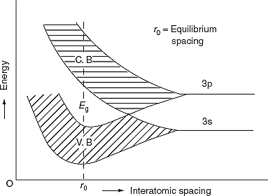
Figure 1
Kronig-Penney model shows the existence of band gap. Kronig-Penney model supports the existence of these bands of energies (allowed bands and forbidden bands).
The formation of energy bands has been explained taking Sodium (Na) metal as an example. When isolated sodium atoms are brought together to form a solid, then the energy levels of the valence electrons spread into bands. The 3S and 3P orbitals electrons energies are shown in Figure 1. These bands are seen to overlap strongly at the interatomic spacing of sodium.
We know that atoms have discrete energy levels. When a huge number of atoms are combined to form a solid, these discrete energy levels are replaced by discrete ranges of energy or called as energy bands.
In energy bands there are so many individual allowed energy values or you can say that the energy bands the energy distribution is continuous. This is shown in the following figure
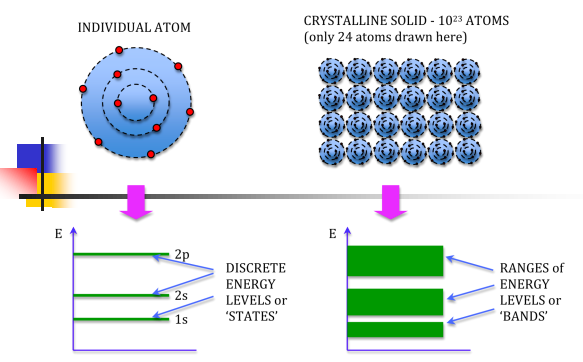
Figure 2
In between energy bands are ranges of energy which are entirely impossible known as band gaps
Different substances have different band structures which explain the characteristics of that substance in terms of electrical conduction.
The Band Model
Bands are formed by the closely spaced orbitals.
There are three types of bands:
1. Valance Bands: Valence band it is a group of orbitals which contain electrons in the shell. Or we can say It is also defined as the energy band that comprises of valence electrons present in the outermost shell of an atomic structure.
These valence electrons, when provided with sufficient energy, get changed into free electrons and moves to conduction band thereby causing conductivity. It is at a lower energy level than the conduction band in the energy level diagram.
2. Conduction Band: Conduction band is a group of empty orbitals of the shells that do not contain any electron due to their configuration making the orbitals of higher energy levels.
When the electrons pass from valance band to the conduction band these solids conduct electricity with flow of charges in the form of electrons.
3. Forbidden Energy Band: These two bands are separated by a certain amount of energy known as the forbidden energy gap. In this band not a single electron is available. It diagram it is named as Band Gap.
Let us distinguish between conductor, semiconductors and insulator on the basis of these bands.
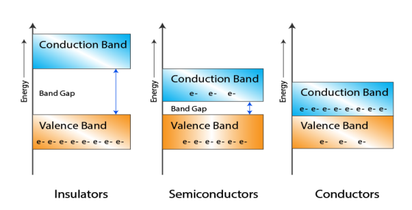
Figure 3
- In Conductors: The valance band and the conduction band overlap each other. This makes it easy for the electricity to pass through them. In conductors, the valence band is either not fully occupied with electrons, or the filled valence band overlaps with the empty conduction band. In general, both states occur at the same time, the electrons can therefore move inside the partially filled valence band or inside the two overlapping bands. In conductors there is no band gap between the valence band and conduction band.
- In Semi-conductors: there is a slight gap between the conduction band and the valance band. This band gap is less than or equal to 1.4 eV. The electrons from valance shell take a little energy to excite from valance band to the conduction band. Even in semiconductors, there is a band gap, but compared to insulators it is so small that even at room temperature electrons from the valence band can be lifted into the conduction band. The electrons can move freely and act as charge carriers.
- In Insulators: In insulators the valence band is fully occupied with electrons due to the covalent bonds. To achieve conductivity, electrons from the valence band have to move into the conduction band. the energy gap is considerably large and the electrons of the valance band cannot be excited to the conduction band before the melting or the dissociation of the solid. This means that under the practically ambient condition it cannot conduct electricity.
Consider an isolated silicon atom; its energy levels are quantized. When two identical atoms are brought closer together, the quantized energy levels hybridize and split into two different levels because of the mutual interaction of the two atoms. More generally, when N atoms are moved closer, until they reach the equilibrium inter-atomic distance d, the energy levels split into N levels. These N levels are very close to each other if N is large (which is the case in a crystal) so that they eventually form a continuous energy band.
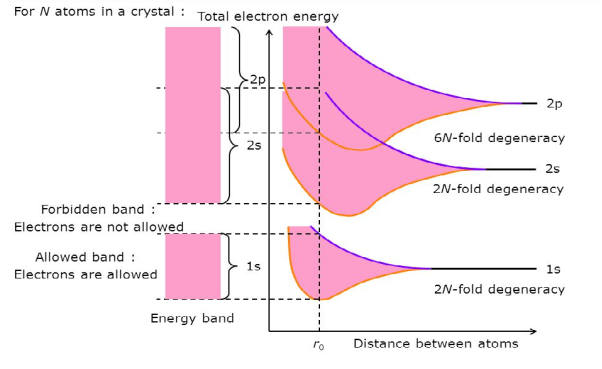
Figure 4: Formation of Energy band as a function of interatomic distance (distance between atoms)
An intrinsic type of semiconductor material made to be very pure chemically. As a result it possesses a very low conductivity level having very few number of charge carriers, namely holes and electrons, which it possesses in equal quantities.
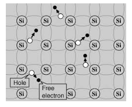
Figure 5
The most commonly used semiconductor basics material by far is silicon. Silicon has four valence electrons in its outermost shell which it shares with its neighbouring silicon atoms to form full orbital’s of eight electrons. The structure of the bond between the two silicon atoms is such that each atom shares one electron with its neighbour making the bond very stable.
As there are very few free electrons available to move around the silicon crystal, crystals of pure silicon (or germanium) are therefore good insulators. Silicon atoms are arranged in a definite symmetrical pattern making them a crystalline solid structure. A crystal of pure silica (silicon dioxide or glass) is generally said to be an intrinsic crystal (it has no impurities) and therefore has no free electrons.
An extremely pure semiconductor is called as Intrinsic Semiconductor. On the basis of the energy band phenomenon, an intrinsic semiconductor at absolute zero temperature is shown below.
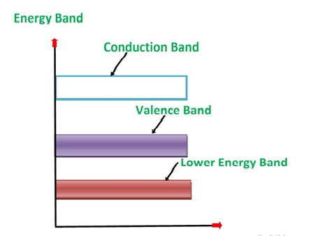
Figure 6
Its valence band is completely filled and the conduction band is completely empty. When the temperature is raised and some heat energy is supplied to it, some of the valence electrons are lifted to conduction band leaving behind holes in the valence band as shown below.
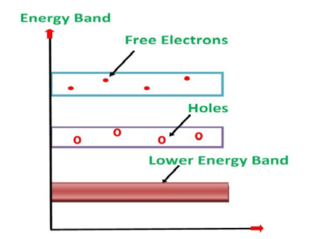
Figure 7
A hole is the absence of an electron in a particular place in an atom. Although it is not a physical particle in the same sense as an electron, a hole can be passed from atom to atom in a semiconductor material. It is considered to have positive charge. Holes are positive charge carriers.
The electrons reaching at the conduction band move randomly. The holes created in the crystal also free to move anywhere.
This behaviour of the semiconductor shows that they have a negative temperature coefficient of resistance. This means that with the increase in temperature, the resistivity of the material decreases and the conductivity increases.
But simply connecting a silicon crystal to a battery supply is not enough to extract an electric current from it. To do that we need to create a “positive” and a “negative” pole within the silicon allowing electrons and therefore electric current to flow out of the silicon. These poles are created by doping the silicon with certain impurities.
Intrinsic semiconductors—carrier concentration
Here we will calculate the number of electrons excited into conduction band at temperature T and also the hole concentration in the valence band. It is assumed that the electrons in the conduction band behave as if they are free particles with effective mass me* and the holes near the top of the valence band behave as if they are free particles with effective mass mh*.
Here we will calculate the electron concentration, hole concentration
Density of Electrons in Conduction Band
The number of free electrons per unit volume of semiconductor having energies in between E and E + dE is represented as N(E) dE
dE = width of Energy band
Therefore, we have:
N(E) dE = ge(E) dE fe(E) ……….(1)
ge(E) = The density of electron states per unit volume
fe(E) = Fermi-Dirac distribution function i.e. probability that an electron occupies an electron state
The number of electrons present in the conduction band per unit volume of material ‘n’ is obtained by integrating N(E) dE between the limits Ec and Ect
Where Ec = the bottom energy levels of conduction band
Ect = the bottom and top energy levels of conduction band
n =  ……….(2)
Can be written as
n =  =
= 
n =  -
-  ……….(3)
We know that above Ect, there is no electrons.
Hence, Equation (3) becomes
n =  -
- 
n =  ……….(4)
The Fermi-Dirac distribution function fe(E) can be represented as:
 (E) =
(E) = ……….(5)
Compared to the exponential value, so the ‘1’ in the denominator can be neglected.
So  >>1
>>1
Hence,  (E) =
(E) = =
=  ……….(6)
The density of electron states ge(E) in the energy space from E = 0 to E can be written as:
 (E) =
(E) =  [
[ ]3/2 (E - 0) ½ ……….(7)
Where me* is the effective mass of an electron and h is Planck’s constant.
 (E)dE =
  [
[ ]3/2 (E - 0) ½dE ……….(8)
To evaluate n, the density of states is counted from Ec, since the minimum energy state in conduction band is Ec. So eq (8) can become
 (E)dE =
  [
[ ]3/2 (E - Ec) ½dE ……….(9)
Substituting Equations (6) and (9) in (4) gives
n =  3/2
3/2 (E-
(E- )1/2
)1/2 dE
dE
n = [
[ ]3/2
]3/2  1/2
1/2 dE ………… (10)
The above equation can be simplified by the following substitution:
Put ɛ = E − Ec ………… (11)
So, dɛ = dE
In Equation (11), Ec is constant, as we change the variable E to ε in Equation (10), the integral limits also change.
In Equation (11), as E → Ec then ε → 0 and E → ∞, then ε also → ∞.
The exponential term in Equation (10) becomes:
 = exp [
 ] = exp [
 ]
]

 ………… (12)
Substituting Equations (11) and (12) in (10), we get:
n = [
[ ]3/2
]3/2  dE
dE
n = [
[ ]3/2
]3/2
 dE ………… (13)
Above integral (I) can be simplified by substitution. Put ε = x2
So that dɛ = 2x dx
I = 2x dx
2x dx
= dx
dx
= =
= T)3/2 ………… (14)
Substituting Equation (14) in (13) gives:
n = [
[ ]3/2
]3/2 T)3/2
T)3/2
n =
n = 
n =  ………… (15)
The term  is almost a constant compared with the exponential term as the temperature changes. So, it is a pseudo constant and is given by the symbol Nc. So, we have
n =Nc ………… (16)
Density of Holes in Valence Band
The number of holes per unit volume of semiconductor in the energy range E and E + dE in valence band is represented as P(E) dE. Proceeding same way( as in case of electrons) we have
Therefore, we have:
P(E) dE = gh(E) dE fh(E) ……….(17)
dE = width of Energy band
gh(E) = The density of holes states per unit volume
fh(E) = Fermi-Dirac distribution function i.e. probability that an hole occupies an electron state
The number of electrons present in the conduction band per unit volume of material ‘n’ is obtained by integrating P(E) dE between the limits Evb and EV
Where EV = the bottom energy levels of valence band
Evb = the bottom and top energy levels of valence band
The total number of holes present in the valence band per unit volume of material ‘p’ is obtained by integrating P(E) dE
 ……….(18)
Equation (18) can be represented as:
 ……….(19)
Now we know that below Evb no holes is present. Hence, Equation (19) becomes
 ……….(20)
We know hole can also be defined as absence of an electron.
Presence of a hole = the absence of an electron
Hence, the Fermi-Dirac function of holes fh(E) in the valence band is:
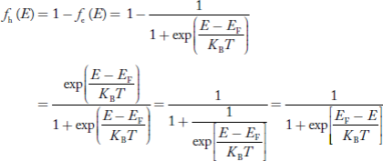
Compared to exponential, the ‘1’ in the denominator is negligible,

Hence,
 ……….(21)
The density of hole states between E and E + dE in valence band can be written similar to Equation (8.9) for electrons.
 ……….(22)
Where mh* is the effective mass of hole.
Substituting Equations (21) and (22) in (20),
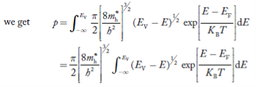 ……….(23)
The above equation can be simplified by the substitution:
Put ɛ = EV − E ............. (24)
So dɛ = − dE
In Equation (24), EV is constant, as we change the variable E to ε in Equation (23), the integral limits also change.
In Equation (24),
As E → EV then ε → 0
And E→ −∞, then ε → ∞
The exponential term in Equation (23) becomes:
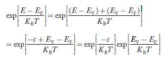 ............. (25)
Substituting Equations (24) and (25) in (23), we get:
 ………….(26)
From Equation (14), we know the integral value  T)3/2 put here and we get
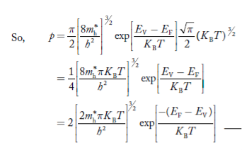 ………….(27)
….The term  is almost constant compared with the exponential term as the temperature changes. So, it is a pseudo constant and is given by the symbol NV. So, we have
 …………… (28)
Fermi Level
We know that in intrinsic semiconductor
Electron concentration ‘n’ = Hole concentration ‘p’
Equating Equations (15) and (27), we get
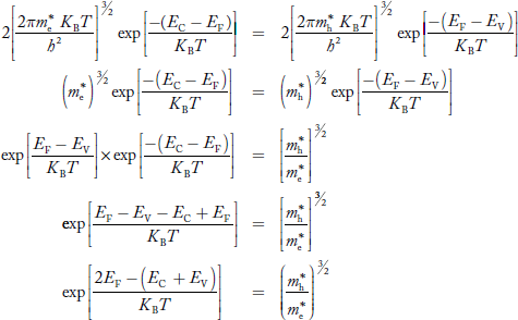
Taking logarithms on both sides, we get
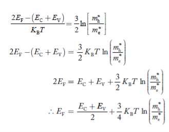 ……………… (29)
Normally, mh* is greater than me*, since ln  is very small so that EF is just lie in the middle of energy gap
Temperature effect on Fermi level
Fermi level slightly rises with increase of temperature.
But in case of pure intrinsic semiconductor like Si and Ge,
mh* ≈ me*
So in these cases Fermi level lies at the middle of energy gap.
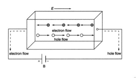
In semiconductor, the conduction band electron and valance band hole participate in electrical conduction. To obtain expression for electrical conductivity consider an intrinsic semiconductor bar which is connected to external battery as shown in figure
The electric field exist along x direction. The field accelerate electrons (conduction electrons) along negative X-direction and holes along positive X-direction. They starts moving with a constant velocity called Drift velocity vd
The total current in the semiconductor (due to both electron and hole)
I = Ie +Ih
Or total current density
J = Je +Jh ..........(1)
8 Figure
In order to find the current density of electrons, let the concentration of electrons are 'n' , charge is 'e' and drift velocity is 've', Then
Je =neve ..........(2)
The drift velocity produced per unit elctric feild is called 'mobility' , Thus
μe = 
Or
μeE = 
Substituting in equation 2
Je =neμeE ..........(3)
From Ohms law,
J = E where Je = eE
Je =neμeE = eE ..........(4)
e = neμe ..........(5)
Similarly current density for holes
Jp =peμpE = pE ..........(6)
And conductivity
p = peμp ..........(7)
Substituting value of Je and Jp from eq 4 and 6 in eq 1, we get
J = neμeE + peμpE
J = (neμe + peμp)E ..........(8)
From Ohms law J = E
= neμe + peμp
Where e = neμe and p = peμp
Also ni =CT3/2e -Eg/2kT ..........(9)
Therefore
= nie(μe + μp) = CT3/2e -Eg/2kT e(μe + μp) ..........(10)
The mobilities of carrier depend upon temperature as
μ 

For Electrons μe
 and for holes μp

μe + μp= =
=  ..........(11)
Using equation 11 in equation 10
= CT3/2e -Eg/2kT e
= C e e -Eg/2kT
Let B = C e we get
= Be -Eg/2kT ..........(12)
Doping
The process by which an impurity is added to a semiconductor is known as Doping. The amount and type of impurity which is to be added to a material has to be closely controlled during the preparation of extrinsic semiconductor. Generally, one impurity atom is added to a 108 atoms of a semiconductor.
The purpose of adding impurity in the semiconductor crystal is to increase the number of free electrons or holes to make it conductive.
If a Pentavalent impurity, having five valence electrons is added to a pure semiconductor a large number of free electrons will exist. Which make a n-type extrinsic semiconductor.
If a trivalent impurity having three valence electrons is added, a large number of holes will exist in the semiconductor. Which make a p-type extrinsic semiconductor.
Extrinsic Semiconductor
Extrinsic types of semiconductor are those where a small amount of impurity has been added to the basic intrinsic material. This 'doping' uses an element from a different periodic table group and in this way it will either have more or less electrons in the valence band than the semiconductor itself. This creates either an excess or shortage of electrons. In this way two types of semiconductor are available: Electrons are negatively charged carriers. Holes are positively charged carriers.
Depending upon the type of impurity added the extrinsic semiconductor may be classified as n type semiconductor and p type semiconductor.
P-type Extrinsic Semiconductor
The extrinsic p-Type Semiconductor is formed when a trivalent impurity is added to a pure semiconductor in a small amount, and as a result, a large number of holes are created in it. A large number of holes are provided in the semiconductor material by the addition of trivalent impurities like Gallium and Indium. Such type of impurities which produces p-type semiconductor are known as an Acceptor Impurities because each atom of them create one hole which can accept one electron.
In a P-type semiconductor material there is a shortage of electrons, i.e. there are 'holes' in the crystal lattice. Electrons may move from one empty position to another and in this case it can be considered that the holes are moving. This can happen under the influence of a potential difference and the holes can be seen to flow in one direction resulting in an electric current flow. It is actually harder for holes to move than for free electrons to move and therefore the mobility of holes is less than that of free electrons. Holes are positively charged carriers.
A trivalent impurity like Aluminium, having three valence electrons is added to Silicon crystal in a small amount. Each atom of the impurity fits in the Silicon crystal in such a way that its three valence electrons form covalent bonds with the three surrounding Silicon atoms as shown in the figure below.
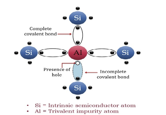
Figure 9
Energy Band Diagram of p-Type Semiconductor
The energy band diagram of a p-Type Semiconductor is shown below.
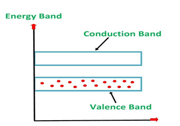
Figure 10
A large number of holes or vacant space in the covalent bond is created in the crystal with the addition of the trivalent impurity. A small or minute quantity of free electrons is also available in the conduction band.
They are produced when thermal energy at room temperature is imparted to the Silicon crystal forming electron-hole pairs. But the holes are more in number as compared to the electrons in the conduction band. It is because of the predominance of holes over electrons that the material is called as a p-type semiconductor. The word “p” stands for the positive material.
Conduction Through p Type Semiconductor
In p type semiconductor large number of holes are created by the trivalent impurity. When a potential difference is applied across this type of semiconductors.
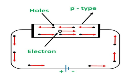
Figure 11
The holes are available in the valence band are directed towards the negative terminal. As the current flow through the crystal is by holes, which are carrier of positive charge, therefore, this type of conductivity is known as positive or p type conductivity. In a p type conductivity the valence electrons move from one covalent to another.
The conductivity of n type semiconductor is nearly double to that of p type semiconductor. The electrons available in the conduction band of the n type semiconductor are much more movable than holes available in the valence band in a p type semiconductor. The mobility of holes is poor as they are more bound to the nucleus.
Even at the room temperature the electron hole pairs are formed. These free electrons which are available in minute quantity also carry a little amount of current in the p type semiconductors.
N-type Extrinsic Semiconductor
When a few Pentavalent impurities such as Phosphorus whose atomic number is 15, which is categorised as 2, 8 and 5. It has five valence electrons, which is added to silicon crystal. Each atom of the impurity fits in four silicon atoms as shown in the figure below.
Hence, each Arsenic atom provides one free electron in the Silicon crystal. Since an extremely small amount of Phosphorus, impurity has a large number of atoms; it provides millions of free electrons for conduction.
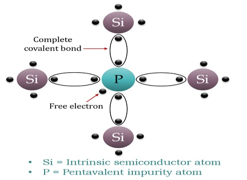
Figure 12
An N-type semiconductor material has an excess of electrons. In this way, free electrons are available within the lattices and their overall movement in one direction under the influence of a potential difference results in an electric current flow. This in an N-type semiconductor, the charge carriers are electrons.
Energy Diagram of n-Type Semiconductor
A large number of free electrons are available in the conduction band because of the addition of the Pentavalent impurity. These electrons are free electrons which did not fit in the covalent bonds of the crystal. However, a minute quantity of free electrons is available in the conduction band forming hole- electron pairs.
The Energy diagram of the n-type semiconductor is shown in the figure below.
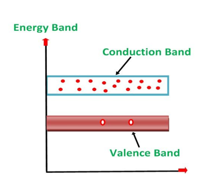
Figure 13
- The addition of pentavalent impurity results in a large number of free electrons.
- When thermal energy at room temperature is imparted to the semiconductor, a hole-electron pair is generated and as a result, a minute quantity of free electrons is available. These electrons leave behind holes in the valence band.
- Here n stands for negative material as the number of free electrons provided by the pentavalent impurity is greater than the number of holes.
Conduction Through n-Type Semiconductor
In the n-type semiconductor, a large number of free electrons are available in the conduction bands which are donated by the impurity atoms. The figure below shows the conduction process of an n-type semiconductor.
When a potential difference is applied across this type of semiconductor, the free electrons are directed towards the positive terminals. It carries an electric current. As the flow of current through the crystal is constituted by free electrons which are carriers of negative charge, therefore, this type of conductivity is known as negative or n-type conductivity.
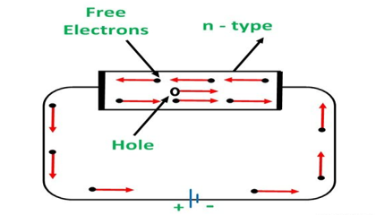
Figure 14
The electron-hole pairs are formed at room temperature. These holes which are available in small quantity in valence band also consist of a small amount of current. For practical purposes, this current is neglected.
Carrier Concentration in Extrinsic Semiconductors
The number of charge carriers present per unit volume of a semiconductor material is called carrier concentration.
Suppose donor and acceptor atoms are doped in a semiconductor.
At temperature T K,
n = number of conduction electrons
p = number of holes
N−A = number of acceptor ions
N+D = number of donor ions
We know that the below equation hold good in semiconductor. The total negative charge due to conduction electrons and acceptor ions is equal to holes and donor ions in unit volume of material.
So the material will be considered neutral if,
n + N−A = p + N+D ……….(34)
Equation (34) is called charge neutrality equation.
In the above equation
 ………..(35)
Concentration of acceptor ions N−A = acceptor concentration x probability of finding an electron in acceptor level
 ………..(36)
Similarly, the donor ions concentration is

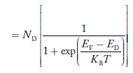 ………..(37)
In n-type material
Note
nn represents electrons in n-type material
pn represents holes concentration in n-type material.
There are no acceptor atoms so N−A = 0.
At 0 K, all the electron states in donor level are occupied by electrons.
As the temperature is increased from 0 K, some of the electrons jump from these donor states into the conduction band.
Also the concentration of holes is extremely less compared with the concentration of conduction electrons [p << n]
From Equation (34) we have
n = p N+D
(Or) n ≈ N+D …………(38) [since p << N+D]
At temperature T K,
As the temperature increase Almost all the donor atoms donate electrons to conduction band.
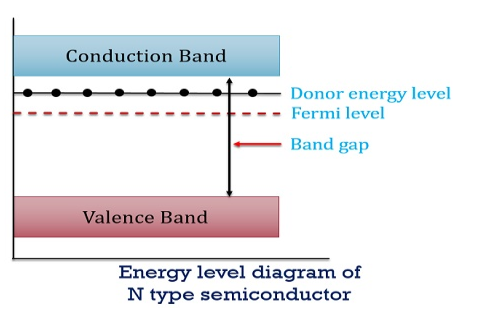
Figure 15
So, in n-type material, the free electron concentration is almost equal to the donor atoms.
So we can rewrite the above equation as
nn ≈ ND …………….(39)
Where nn represents electrons in n-type material
Also the hole concentration in n-type material can be obtained by applying law of mass action nn pn =ni2
 …………..(40)
Where pn represents holes concentration in n-type material.
In n-type material at 0 K, the Fermi energy level lies in the middle of Ec and ED

At temperature> 0K
 ……….(41)
With increase in temperature the Fermi level shifts upwards according to Equation (61) slightly due to ionization of donor atoms.
With further increase of temperature, electron-hole pairs are generated due to the breaking of covalent bonds, hence Fermi level shifts downwards.
In p-type semiconductor
Note
pp represents holes in p-type material
np represents electrons in p-type material
There are no donor atoms so means no ions present  = 0.
= 0.
At 0 K, all the acceptor levels are not occupied by electrons.
As the temperature is increased from 0 K, some electrons jump from top valence band energy levels to the acceptor states, leaving holes in the valence band and acceptor ions  are formed.
At some room temperature T K, concentration of conduction electrons is extremely less compared with hole concentration.
∴ From Equation (34), we have
n + N−A = p ……………(42)
(or) N−A ≈ p ……………. (43) [since n << N−A]
At temperature T K, in p-type material,
The hole concentration is almost equal to the acceptor atoms in unit volume of the material.
So, Equation (43) can be written as
pp ≈ NA ……………….(44)
Where pp represents holes in p-type material
The electron concentration in p-type material can be obtained by applying law of mass action as nppp = ni2
 …………….(45)
Where np represent free electron concentration in p-type material.
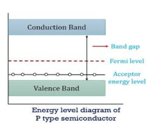
Figure 16
In p-type material, the Fermi level lies in between EV and EA at 0 K

As the temperature is increased from 0 K, the Fermi level shifts downwards slightly as per Equation (46) due to ionization of acceptor atoms.
And with further increase of temperature, electron-hole pairs are generated due to the breaking of covalent bonds, so Fermi level shifts upwards.
There may be two separate bands: a conduction band for electrons and a valence band for holes as shown in Figure 14 (a). In many semiconductors such as Si and PbTe, there may be also multiple bands that have the same energy levels, whereby it is called degeneracy. The heavy and light holes are degenerate and the split-off hole in the valence band is slightly off the valence band edge (maximum).
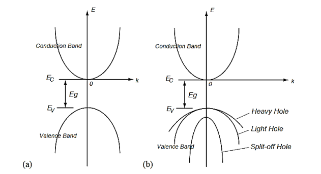
Figure 17: Band structures of a semiconductor including the conduction band and the valence bands.(a) A model of a conduction band and a valence band, and (b) a model of multiple bands.
The type of band gap in semiconductors is important for the selection of material for many electronic devices including thermoelectric devices, solar cells and lasers. There are two types of band gaps in semiconductors, which are direct and indirect band gap. The energy E of a particle is always associated with a wavevector k (or momentum), which implies that, for any transition between bands, both energy and momentum must be conserved. When an electron absorbs enough energy to exceed the energy gap Eg, the electron can jump from the valence band into the conduction band. The source of the energy could be photons, phonons, or electric field.
In direct band gap semiconductors, such as GaAs, the maximum and minimum of energy versus momentum relationship occur at the same value of the wavevector (Figure 15)
In indirect band gap semiconductors like Si and Ge, the maximum and minimum of the energy versus momentum relationship occurs at different wavevectors, which is pictured in Figure 15(b). In this case, the electron cannot directly jump into the conduction band, but once the electron at the valence band edge EV absorbs energy (photon, phonon, or electric field) and reaches the energy level of the conduction band edge EC across the energy band Eg, it can indirectly jump into the conduction band with the aid of phonon energy because phonon usually exists anyway.
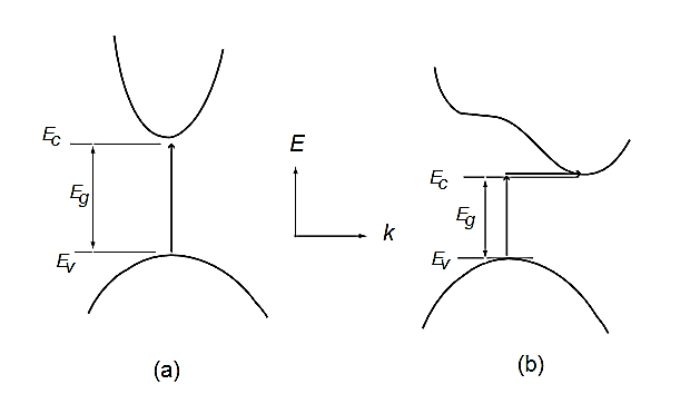
Figure 18: Energy versus wavevector diagrams in (a) direct band gap and (b) indirect band gap semiconductors
Direct and indirect gap semiconductors have major differences in their optical properties. Direct band gap semiconductors are more efficient photon emitters, semiconductor lasers are made of direct gap semiconductors such as GaAs, whereas most electronic devices including thermoelectric devices are built on indirect semiconductors.
The band gap represents the minimum energy difference between the top of the valence band and the bottom of the conduction band, however, the top of the valence band and the bottom of the conduction band are not generally at the same value of the electron momentum. In a direct band gap semiconductor, the top of the valence band and the bottom of the conduction band occur at the same value of momentum, as in the schematic below.
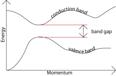
Figure 19
In an indirect band gap semiconductor, the maximum energy of the valence band occurs at a different value of momentum to the minimum in the conduction band energy:
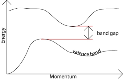
Figure 20
Photon can provide the energy to produce an electron-hole pair. Each photon of energy E has momentum p = E / c, where c is the velocity of light. An optical photon has energy of the order of 10–19 J, and, since c = 3 × 10⁸ ms–1, a typical photon has a very small amount of momentum.
A photon of energy Eg, where Eg is the band gap energy, can produce an electron-hole pair in a direct band gap semiconductor quite easily, because the electron does not need to be given very much momentum. However, an electron must also undergo a significant change in its momentum for a photon of energy Eg to produce an electron-hole pair in an indirect band gap semiconductor. This is possible, but it requires such an electron to interact not only with the photon to gain energy, but also with a lattice vibration called a phonon in order to either gain or lose momentum.
The indirect process proceeds at a much slower rate, as it requires three entities to intersect in order to proceed: an electron, a photon and a phonon. This is analogous to chemical reactions, where, in a particular reaction step, a reaction between two molecules will proceed at a much greater rate than a process which involves three molecules.
The same principle applies to recombination of electrons and holes to produce photons. The recombination process is much more efficient for a direct band gap semiconductor than for an indirect band gap semiconductor, where the process must be mediated by a phonon.
As a result of such considerations, gallium arsenide and other direct band gap semiconductors are used to make optical devices such as LEDs and semiconductor lasers, whereas silicon, which is an indirect band gap semiconductor, is not. The table in the next section lists a number of different semiconducting compounds and their band gaps, and it also specifies whether their band gaps are direct or indirect.
Table :I
| Material | Direct / Indirect Bandgap | Band Gap Energy at 300 K (eV) |
|
|
|
|
Groups III-V compounds | GaAs | Direct | 1.42 |
Groups IV-IV compounds | α-SiC | Indirect | 2.99 |
Groups II-VI compounds | ZnO | Direct | 3.35 |
When magnetic field is applied perpendicular to a current-carrying conductor, then a voltage is developed in the material perpendicular to both magnetic field and current in the conductor. This effect is known as Hall Effect and the voltage developed is known as Hall voltage (VH).
Hall Effect is useful to identify the nature of charge carriers in a material and hence to decide whether the material is n-type semiconductor or p-type semiconductor, also to calculate carrier concentration and mobility of carriers.
Hall Effect can be explained by considering a rectangular block of an extrinsic semiconductor in which current is flowing along the positive X-direction and magnetic field B is applied along Z-direction as shown in Figure.
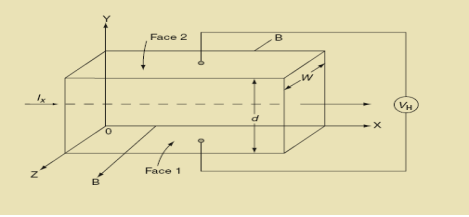
21 Figure: Hall Effect
Suppose if the semiconductor is n-type, then mostly the carriers are electrons and the electric current is due to the drifting of electrons along negative X-direction or if the semiconductor is p-type, then mostly the carriers are holes and the electric current is due to drifting of the holes along positive X-direction.
As these carriers are moving in magnetic field in the semiconductor that mean they experience Lorentz force represented by FL
FL = Bevd
Where vd is the drift velocity of the carriers. (already explained in previous section).
We can obtain the direction of this force by applying Fleming’s left-hand rule in electromagnetism.
Fleming’s left-hand rule can be explained as If we stretch the thumb, fore finger and middle finger in three perpendicular directions so that the fore finger is parallel to the magnetic field and the middle finger is parallel to the current direction, then thumb represents the direction of force on the current-carrying carriers.
So the Lorentz force is exerted on the carriers in the negative Y-direction. Due to Lorentz force, more and more carriers will be deposited at the bottom face (represented by face 1in figure) of the conductor.
The deposition of carriers at the bottom face is continued till the repulsive force due to accumulated charge balances the Lorentz force.
After some time of the applied voltage, both the forces become equal in magnitude and act in opposite direction, then the potential difference between the top and bottom faces is equal to Hall voltage and that can be measured.
At equilibrium, the Lorentz force on a carrier
FL = Bevd ……………..(1)
And the Hall force
FH = eEH ……………..(2)
Where EH is the Hall electric field due to accumulated charge.
At equilibrium, FH = FL
EEH = Bevd
∴ EH = Bvd ……………..(3)
If ‘d’ is the distance between the upper and lower surfaces of the slab, then the Hall field
EH =  ……………..(4)
In n-type material, Jx = –nevd
vd = -  ……………..(5)
Where n is free electron concentration, substituting (5) in (3), we have
∴ EH = -B  ……………..(6)
For a given semiconductor, the Hall field EH is proportional to the current density Jx and the intensity of magnetic field ‘B’ in the material.
i.e. EH ∝ JxB
(or) EH = RHJxB ……………..(7)
Where RH = Hall coefficient
Equations (6) and (7) are same so, we have
RHJxB =-B 
RH = -  = -
= -  ……………..(8)
Where ρ is charge density
Similarly for p-type material
RH =  =
= ……………..(9)
Using Equations (8) and (9), carrier concentration can be determined.
Thus, the Hall coefficient is negative for n-type material. In n-type material, as more negative charge is deposited at the bottom surface, so the top face acquires positive polarity and the Hall field is along negative Y-direction. The polarity at the top and bottom faces can be measured by applying probes.
Similarly, in case of p-type material, more positive charge is deposited at the bottom surface. So, the top face acquires negative polarity and the Hall field is along positive Y-direction. Thus, the sign of Hall coefficient decides the nature of (n-type or p-type) material.
The Hall coefficient can be determined experimentally in the following way:
Multiplying Equation (7) with ‘d’, we have
EHd = VH = RHJxBd ……………..(10)
From (Figure 11) we know the current density Jx
Jx = 
Where W is width of the box. Then, Equation (10) becomes
VH = RH Bd = RH
RH =  ……………..(11)
Substituting the measured values of VH, Ix, B and W in Equation(11), RH is obtained. The polarity of VH will be opposite for n- and p-type semiconductors.
The mobility of charge carriers can be found by using the Hall effect, for example, the conductivity of electrons is
n = neμn
Or we can rewrite it as
μn =  =n RH ……………..(12)
By using equation (11)
μn = n ……………..(13)
• Using magnetic flux leakage – In order to properly inspect items such as pipes or tubes, Hall Effect probes work with something called magnetic flux leakage. This is a way of testing such items, and being able to spot potential corrosion, erosion, or pitting. This is specifically used in steel items, and can give important information about lifespan or safety.
• Sensors to detect rotation speed – A Hall Effect probe can be used to in bicycle wheels, speedometers in the automotive world, electronic types of ignition systems, and gear teeth.
• Used to detected movement – You will often find a Hall Effect probe used in such items as Go-Kart controls, smart phones, paintball guns, or airsoft guns, as well as some GPS systems.
• Ferrite Toroid Hall Effect current transducers – This is mainly used in electronic compasses, making use of the magnetic field to show direction.
• Split-ring clamp-on sensors – These types of Hall Effect probes are used to test equipment without having to take the whole circuit board apart, e.g. Complex items.
• Analog multiplication – Anything which needs a power measurement, e.g. Sensing, and also used in small computers.
• General power measurement – Basically any device which needs to be tested for its power input can be done by a Hall Effect probe.
• Position and motion sensors – This is mainly used in a DC motor, often the brushless type.
• The automotive world – Hall Effect probes are used widely in the automotive world, especially in fuel injection and ignition. Wheel rotation sensors also use Hall Effect probes, e.g. For anti-lock braking.
- For determination of type of given semiconductor.
- For N-type, Hall coefficient RH= negative
- For P-type, Hall coefficient RH= Positive
- To determine carrier concentration n and p; that is n=p=1/e𝑅𝐻
- Determination of mobility of charge carriers μn =
 =n RH. Where 𝜎= electrical conductivity
 - To determine the sign of charge carriers whether the conductivity is due to electrons or holes.
Main Advantages of Using Hall Sensors
Why is a Hall Effect probe advantageous in all of these instances? Because the probes are not affected by outside influences, e.g. Water or dirt. They can also easily sense the measure the output they need when they are placed in the right position. On top of this, Hall Effect probes are safer, because the voltage never actually makes it directly to the sensor/probe. This makes this type of measurement overall so much safer than other methods.
As you can see, understanding how something is put in practice in the real world really helps you to understand it in real terms. The Hall Effect is certainly very common place these days, in much more methods and applications than we realize. While certainly very useful in the automation world, even basic items such as a compass make large use of this scientific approach.
Semiconductors are employed in the manufacture of various kinds of electronic devices, including diodes, transistors, and integrated circuits. Such devices have found wide application because of their compactness, reliability, power efficiency, and low cost.
- Temperature sensors are made with semiconductor devices.
- They are used in 3D printing machines
- Used in microchips and self-driving cars
- Used in calculators, solar plates, computers and other electronic devices.
- Transistor and MOSFET used as a switch in Electrical Circuits are manufactured using the semiconductors.
- The physical and chemical properties of semiconductors make them capable of designing technological wonders like microchips, transistors, LEDs, solar cells, etc.
- The microprocessor used for controlling the operation of space vehicles, trains, robots, etc is made up of transistors and other controlling devices which are manufactured by semiconductor materials.
Semiconductor devices such as diodes, transistors and integrated circuits can be found everywhere in our daily lives, in, televisions, automobiles, washing machines and computers. We have come to be dependent on them. It is widely used because of high performance at low cost.
Semiconductors are used in almost all electronic devices. Their reliability, compactness, low cost and controlled conduction of electricity make them ideal to be used for various purposes in a wide range of components and devices. Transistors, diodes, photosensors, microcontrollers, integrated chips and much more are made up of semiconductors.
Common analog circuits include oscillators and amplifiers. The circuits that interface or translate between analog circuits and digital circuits are known as the mixed-signal circuits.
These are discrete components which are used in power devices, compactness optical sensors, and light emitters, including solid-state lasers. They have a wide range of current and voltage handling capabilities, with current ratings more than 5,000 amperes and voltage ratings more than 100,000 volts. More importantly, semiconductor devices lend themselves to integration into complex but readily build-up microelectronic circuits. They are having probable future, the key elements of the majority of electronic systems including communications with data-processing, consumer, and industrial-control equipment.