UNIT – V
SUPERCONDUCTORS AND NANO MATERIALS
It was first discovered by the Dutch physicist Heike Kamerlingh Onnes, who was the first to liquefy helium (which boils at 4.2 Kelvin at standard pressure).
In 1911 Kamerlingh Onnes and one of his assistants discovered the phenomenon of superconductivity while studying the resistance of metals at low temperatures. They studied mercury because very pure samples could easily be prepared by distillation. The historic measurement of superconductivity in mercury is shown in Figure.
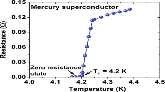
Figure 1
The electrical resistance of mercury decreased steadily upon cooling, but dropped suddenly at 4.2 K, and became undetectably small.
Transition Temperature or Critical Temperature Tc
The temperature at which electrical resistivity of the material suddenly drops to zero and the material changes from normal conductor to a superconductor is called the transition temperature or critical temperature Tc.
Soon after this discovery, many other elemental metals were found to exhibit zero resistance when their temperatures were lowered below a certain characteristic temperature of the material, called the critical temperature, Tc.
Superconductivity
The ability of certain metals, their compounds and alloys to conduct electricity with zero resistance at very low temperature is called superconductivity. The materials which exhibit this property are called superconductors.
PROPERTIES
Following properties are shown by superconductors.
- It is a low temperature phenomenon.
- The electrical resistivity drops to zero.
- The conductivity becomes infinity.
- The transition temperature is different for different substances.
- Material having high normal resistivity exhibit superconductivity.
- Materials for which ρZ= 106 (where Z is a atomic number and ρ is resistivity) show superconductivity.
- Superconductivity is very sharp for chemically pure and structurally perfect specimen.
- Ferro magnetic and Anti ferromagnetic materials are not superconductors.
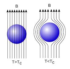
- Below the transition temperature the magnetic flux lines are rejected out of the superconductors.
- Generally Superconducting elements lie in the inner columns of the periodic table.
- Those metallic elements having their valence electrons lies between 2 to 8 exhibit superconductivity.
- Below the transition temperature the specific heat curve is discontinuous.
- There is a discontinuous change in specific heat.
- There are small changes in volume and thermal conductivity of the material.
Superconductivity of a metal mainly depends on the temperature and strength of the magnetic field in which the metal is placed. Superconductivity disappears if the temperature of the specimen is raised above Tc or a strong enough magnetic field is applied. At temperatures below Tc, in the absence of magnetic field, the material is in superconducting state. When the strength of the magnetic field is applied to a critical value Hc the superconductivity disappears.
Critical Temperature for Superconductors
The critical temperature for superconductors is the temperature at which the electrical resistivity of a metal drops to zero. The transition is so sudden and complete that it appears to be a transition to a different phase of matter; this superconducting phase is described by the BCS theory. Several materials exhibit superconducting phase transitions at low temperatures. The highest critical temperature was about 23 K until the discovery in 1986 of some high temperature superconductors.
Materials with critical temperatures in the range 120 K have received a great deal of attention because they can be maintained in the superconducting state with liquid nitrogen (77 K).
Critical Magnetic Field
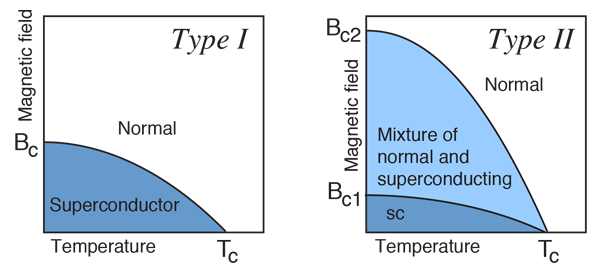
The superconducting state cannot exist in the presence of a magnetic field greater than a critical value, even at absolute zero. This critical magnetic field is strongly correlated with the critical temperature for the superconductor, which is in turn correlated with the bandgap. Type II superconductors show two critical magnetic field values, one at the onset of a mixed superconducting and normal state and one where superconductivity ceases.
It is the nature of superconductors to exclude magnetic fields (Meissner effect) so long as the applied field does not exceed their critical magnetic field. This critical magnetic field is tabulated for 0K and decreases from that magnitude with increasing temperature, reaching zero at the critical temperature for superconductivity. The critical magnetic field at any temperature below the critical temperature is given by the relationship
The dependence of critical field upon the temperature is given by
HC(T) = HC(0) [ 1 – (T/TC)2]
In 1933, Walter Meissner and Robert Ochsenfeld discovered a magnetic phenomenon that showed that superconductors are not just perfect conductors.
When a weak magnetic is applied to a superconducting specimen at a temperature below transition temperature Tc the magnetic flux lines are expelled. This phenomenon is called Meissner effect.
Under normal state the magnetic induction inside the specimen is
B = μ0(H+I)
Where H is the external applied magnetic field and I is the magnetization produced inside the specimen.
When the specimen is in superconducting state B=0 (Meissner effect)
B = μ0(H+I)
0 = μ0(H+I)
H= -I
χ = H/I =-1
Thus the material is act as a perfectly diamagnetic because for diamagnetic material susceptibility χ = -1 .
Let us consider a superconducting material is in normal state. From ohms law, the electric field E=Jρ
On cooling the material to its transition temperature ρ tends to zero. If J is held finite E must be zero. From Maxwell’s equations
∇ × E = - dB / dt
Under superconducting condition
Since E is zero
DB/dt =0
Or B=constant.
This means that the magnetic flux passing through the specimen should not change on cooling to the transition temperature. The Meissner effect contradicts the result.
Application of Meissner Effect
This effect of superconductivity is used in magnetic levitation which is the base of modern high-speed bullet trains. In superconducting state (phase), due to expulsion of external magnetic field, the sample of superconducting material levitates above magnet or vice-versa. Modern high-speed bullet trains use the phenomenon of magnetic levitation.
BCS theory of superconductor was put forward by Bardeen, Cooper and Schrieffer in 1957 and hence named as BCS theory. This theory could explain the effects such as zero resistivity, Meissner effect, isotopic effect etc. Electron lattice interaction via lattice deformation.
Electron –phonon Interaction
BCS theory showed that the basic interaction responsible for superconductivity appears to be that of a pair of electrons by means of an interchange of virtual phonons. This is explained as follows:-
Suppose an electron approaches a positive ion core. It suffers attractive coulomb interaction. Due to this attraction ion core is set in motion and thus distorts that lattice. Let a second electron come in the way of distorted lattice and interaction between the two occurs which lowers the energy of the second electron. The two electrons therefore interact indirectly, via lattice distortion or the phonon field, thus lowering the energy of electrons. This type of interaction is called electron-lattice is quantized in terms of phonons the above interaction can also be interpreted as electron –electron interaction through phonons.
Let an electron of wave vector K emits phonon q, which is absorbed by an electron of wave number K. K is thus scattered as K-q and the process being a virtual one. The nature of the resulting electron-electron interactions depends on the relative magnitudes of the electronic energy change and the phonon energy. If this phonon energy exceeds electronic energy, the interaction is attractive.
Let us consider an electron is passing through the lattice positive ions. The electron is attracted by the neighbouring lattice positive ions as shown in figure 1. Due to the attraction of electron and ion core, the lattice gets deformed on scale. So electron get partially positive charge. Now if another electron passes by the side of assembly of said electron and ion core, it gets attracted towards the assembly.
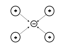
Figure 9
The second electron interacts with the first electron due to the exchange of virtual photon q, between two electrons. The interaction process can be written in terms the wave vector k as
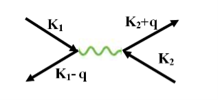
Figure 10
k1’ =k1–q k2’ = k2+q
These two electrons together form a cooper pair and is known as cooper electron.
Cooper pairs
To understand the mechanism of cooper pair formation, let us consider the distribution of electrons in metals as given by the Fermi-Dirac distribution function.
F(E) = 1/ 1+ e E-EF/kT
At T= 0K, all the Fermi energy states below the Fermi level are completely filled and all the states above are completely empty. Let us see what happens when two electrons are added to a metal at absolute zero. Since all the quantum states E<EF, are filled, they are forced to occupy states having E>EF.
Cooper showed that if there an attraction between the two electrons, they are able to form a bound state so that their total energy is less than 2EF. These two electrons are paired to form a single system. These two electrons form a cooper pair and is known as cooper electron.
Coherence length
The paired electrons are not scattered and can maintain their coupled motion up to certain distance called the coherence length. It is a measure of the distance within which the gap parameter does not change very much in varying magnetic field.
Josephson Effect
Let us consider a thin insulation layer is sandwiched between the two superconductors in addition to normal tunneling of electrons, the super electrons tunnel through the insulation layer from one superconductor to another with dissociation, even at zero potential difference across the junction. Their wave functions on both sides are highly correlated. This is known as Josephson Effect.
D.C Josephson effect
According to Josephson when tunnelling across through the insulator it introduces a phase difference ϕ0 between the two parts of the function on opposite sides of the junction as shown in figure
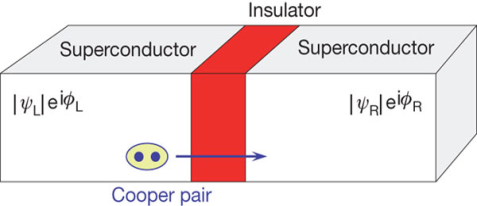
Figure 12
The tunnelling current is given by
I =I0 Sin(ϕ0)
Where I0 is the maximum current that flows through the junction without any potential difference across the junction. This effect is called D.C Josephson effect.
Mathematical Analysis
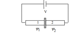
Figure 13: Two superconductors separated by a thin insulator
Suppose we have two superconductors connected by a thin layer of insulating material as shown in figure. We define Ψ1 and Ψ2 as the quantum mechanical wave function of the superconducting state in the left and the right superconductor. The dynamics of the two wave functions are then determined by the following coupled Schrödinger equations:
iℏ  = µ1 Ψ1 +K Ψ2
iℏ  = µ2 Ψ2 +K Ψ1 …….(1)
Where K is constant representing the coupling across the barrier.
And µ1, µ2 are the lowest energy states on either side.
The wavefunctions can be written as
Ψ1 = 

Ψ2 = 
 …….(2)
Where n1, n2 are the density of Cooper pairs and θ are the phases. Substituting equation (2) into equation (1) gives
ℏ  = -ℏ
= -ℏ  = 2K
= 2K  Sin(θ2- θ1) …….(3)
ℏ  (θ2- θ1) = µ2 - µ1 …….(4)
The time derivative of the density of Cooper pairs describes a charge transport therefore I = ∂n1/∂t.
If a voltage V is applied between the junctions the energy levels will shift that is µ2 −µ1 = 2eV .
Let I0 = 2K (n1n2) ½/ ℏ and ϕ0= θ1 – θ2 then
I =I0 Sin ϕ0 …….(5)
 =2eV /ℏ …….(6)
Equations (5) and (6) provide the main results of Josephson junction theory. The current I is called a Josephson current or a super current. This strongly predicts non-linear current-voltage behavior.
From equation (5,6) it is clear that DC current can be drawn through the junction without any voltage drop, as long as the DC current is smaller than I0.
The phase difference will adjust according to equation (5).
A.C Josephson effect
Let a static potential difference is applied across the junction, an additional phase is introduced by the cooper pairs during tunnelling across the junction. This additional phase change ∆ϕ at any time t can be calculated using quantum mechanics.
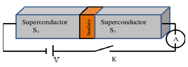
Figure 14:
∆ϕ = Et /ℏ
Where E denotes the total energy of the system.
In present case E=2eV0
Hence
∆ϕ = 2eV0t /ℏ
The tunneling current can be written as
I = I0 Sin(ϕ0 +2eV0t /ℏ)
I = I0 Sin(ϕ0 +ωt )
Where ω = 2eV0/ℏ
This represents alternating current with angular frequency ω. This is A.C Josephson effect.
Current voltage characteristic of a junction is shown in figure.
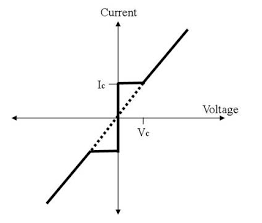
Figure 15:
When Vo = 0 there is a constant flow of dc current through the junction.
This current is called superconducting current and the effect is called Josephson effect.
When Vo < Vc, a constant dc current Ic flows.
When Vo > Vc, the junction has finite resistance, and the current oscillates with some frequency.
Applications of Josephson Effect
- Josephson effect is used to generate microwaves frequency with ω = 2eV0/ℏ
- A.C Josephson effect is used to define standard volt.
- A.C Josephson effect is used to measure very low temperatures based on the variation of frequency of the emitted radiation with temperature.
- A.C Josephson effect is used for switching of signals from one circuit to another.
Types of Superconductors
Based on the diamagnetic response superconductors can be classified into two types, they are
1. Type I superconductors
2. Type II superconductors.
- Type I superconductors
Superconductors which one follows a complete Meissner effect is called type I superconductors. It is also known as soft superconductors.
When the magnetic field strength is gradually increased from its initial value H < HC at HC the diamagnetism is abruptly disappear and the transition from superconducting state to normal state is sharp as shown in figure. These superconductors are known as soft superconductors.
Examples: - Al, Zn, Hg and Sn
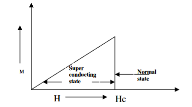
Figure 2: Type I superconductors
2. Type II superconductors
Superconductors which does not follow the complete Meissner effect is called type I superconductors. It is also known as hard superconductors.
In type II superconductors, the specimen is in pure superconducting state up to the field HC1 (lower critical field) when the field is increased beyond HC2 (upper critical state) the magnetic flux lines start penetrating.
The specimen is in mixed state between HC1 and HC2. Above HC2, the specimen is in normal state. This means that the Meissner effect is incomplete in the region between HC1 and HC2. This region is known as vertex region. These superconductors are known as hard superconductors.
Examples: - Zr, Nb

Figure 3: Type II superconductors
Differences between type I and Type II superconductor
Type I superconductor | Type II superconductor |
1. It follows complete Meissner effect. | 1. It does not follow the complete Meissner effect |
2. It has single critical field valueHC | 2. It has two critical field values HC1 and HC2. |
3. There no mixed state. | 3. There is a mixed state |
4. They are soft superconductors | 4. They are hard superconductors |
5. Materials with pure form are type I superconductors | 5. Materials with impurities or alloys are type II superconductors |
Types of Superconductors
Based on the diamagnetic response superconductors can be classified into two types, they are
1. Type I superconductors
2. Type II superconductors.
- Type I superconductors
Superconductors which one follows a complete Meissner effect is called type I superconductors. It is also known as soft superconductors.
When the magnetic field strength is gradually increased from its initial value H < HC at HC the diamagnetism is abruptly disappear and the transition from superconducting state to normal state is sharp as shown in figure. These superconductors are known as soft superconductors.
Examples: - Al, Zn, Hg and Sn

Figure 2: Type I superconductors
2. Type II superconductors
Superconductors which does not follow the complete Meissner effect is called type I superconductors. It is also known as hard superconductors.
In type II superconductors, the specimen is in pure superconducting state up to the field HC1 (lower critical field) when the field is increased beyond HC2 (upper critical state) the magnetic flux lines start penetrating.
The specimen is in mixed state between HC1 and HC2. Above HC2, the specimen is in normal state. This means that the Meissner effect is incomplete in the region between HC1 and HC2. This region is known as vertex region. These superconductors are known as hard superconductors.
Examples: - Zr, Nb
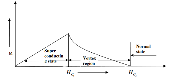
Figure 3: Type II superconductors
Differences between type I and Type II superconductor
Type I superconductor | Type II superconductor |
1. It follows complete Meissner effect. | 1. It does not follow the complete Meissner effect |
2. It has single critical field valueHC | 2. It has two critical field values HC1 and HC2. |
3. There no mixed state. | 3. There is a mixed state |
4. They are soft superconductors | 4. They are hard superconductors |
5. Materials with pure form are type I superconductors | 5. Materials with impurities or alloys are type II superconductors |
The high-Tc superconductors are the class of materials with the highest recorded transition temperatures, on the order of 100 K and above. Discovered over 20 years ago, there remain number of unanswered questions about these compounds.
The first high temperature superconductor was discovered in 1986, by IBM researchers Bednorz and Müller, who were awarded the Nobel Prize in Physics in 1987 "for their important break-through in the discovery of superconductivity in ceramic materials".
High-temperature superconductors (abbreviated high-Tc or HTS) are operatively defined as materials that behave as superconductors at temperatures above 77 K (−196.2 °C; −321.1 °F), the boiling point of liquid nitrogen, one of the simplest coolants in cryogenics. All superconducting materials known at ordinary pressures currently work far below ambient temperatures and therefore require cooling. The majority of high-temperature superconductors are ceramic materials. On the other hand, Metallic superconductors usually work below -200 °C: they are then called low-temperature superconductors. Metallic superconductors are also ordinary superconductors, since they were discovered and used before the high-temperature ones.
Ceramic superconductors are now becoming suitable for some practical use, but they still have many manufacturing issues and there are very few successful practical examples of employment. Most ceramics are brittle which makes the fabrication of wires from them very problematic.
The major advantage of high-temperature ceramic superconductors is that they can be cooled by using liquid nitrogen. On the other hand, metallic superconductors usually require more difficult coolants - mostly liquid helium. Unfortunately, none of high-temperature superconductors are cool able using only dry ice, and none of them works at room temperature and pressure (they work well below the lowest temperature recorded on Earth). All high-temperature superconductors require some kind of cooling systems.
The main class of high-temperature superconductors are in the class of copper oxides (only some particular copper oxides). The second class of high-temperature superconductors in the practical classification is the class of iron-based compounds. Magnesium diboride is sometimes included in high-temperature superconductors: it is relatively simple to manufacture, but it super conducts only below −230 °C, which makes it unsuitable for liquid nitrogen cooling (approximately 30 °C below nitrogen triple point temperature). For example, it can be cooled with liquid helium, which works at much lower temperatures.
Many ceramic superconductors physically behave as superconductors of the second type.
Some extremely-high pressure super hydride compounds are usually categorized as high-temperature superconductors. In fact, many articles on high-temperature superconductors can be found on this research on high pressure gases, which is not suitable for practical applications. The current TC record holder is lanthanum decahydride.
One of the key mysteries surrounds the identity of the so-called 'pseudo gap' region of the phase diagram. In this regime there exists a gap like feature observed in many physical quantities, yet there is no obvious signs of an ordered phase. Some of the research in the group has been directed at studying the specific heat of the high-Tc's in the pseudogap region of the phase diagram.
A second intriguing question surrounds how the high-Tc's evolve with charge carrier concentration (doping), moving from an antiferromagnetically ordered insulator at low doping, to an unconventional superconductor and eventually a Fermi liquid metal at higher doping. At low dopings, there is evidence for a 'glassy' behaviour of electronic spins, and part of the research effort is directed towards exploring this region of the phase diagram through muon-spin relaxation, transport and dielectric measurements.
- Superconductors form the basis of energy saving power systems, namely the superconducting generators, which are smaller in size and weight, in comparison with conventional generators.
- Superconducting magnetic propulsion systems may be used to launch satellites into orbits directly from the earth without the use of rockets.
- High-efficiency ore-separating machines may be built using superconducting magnets which can be used to separate tumour cells from healthy cells by high gradient magnetic separation method.
- Since the current in a superconducting wire can flow without any change in magnitude, it can be used for transmission lines.
- Superconductors can be used as memory or storage elements in computers.
- If you set up a current in a loop of superconductor there is nothing to stop it and it will continue flowing forever, forming a very powerful electromagnet, that needs no maintenance other than keeping them cold. The strongest man made permanent magnetic fields are produced using superconductors.
- Superconducting magnets are used in MRI (Magentic Resonance Imaging) which is a way of looking at the soft parts of the body.
- They are also going to be used in the new ‘Large Hadron Collider’ experiment at the CERN Particle Physics Lab. The idea is to accelerate protons and antiprotons to almost the speed of light in a circle and then smash them together. To keep the particles in a circle requires huge magnetic fields which can only be provided by superconductors.
- It is also possible to use superconducting magnets to produce a levitating train. The idea is to put very powerful light superconducting magnets on the train, then use copper coils in the track which use repulsion to lift the train up to make it levitate. It is also possible to use the track magnets to push the train along. Because this force is not limited by friction between wheels and a track it is theoretically possible for a maglev train to go much faster and more importantly accelerate and brake faster than a conventional train. Various test maglev trains have been built, in Birmingham, Japan and Germany, although the only one used commercially is a german design built in Shanghi, which uses very strong permanent magnets instead of superconductors.
- Due to a subtlety of the quantum mechanics of how superconductors interact with magnetic fields, it is possible to make the most sensitive magnetometers possible called SQUIDs (Superconducting Quantum Interference Devices). These can be used to detect submarines, measure the magnetic field produced by your brain, find ore deposits deep underground, sense minute signals from stars etc.
- An obvious use of superconductors would be to move power around, huge amounts of electrical energy are wasted just heating up power cables, and superconductors would help. However if you put alternating current through them they are no longer lossless, and it requires a lot of energy to cool them, so although it is possible they could be used to save energy in the long run in the short term it is more likely they will be used to save space, superconducting cables have been installed in Chicago and Copenhagen, in old cable ducts with restricted space, allowing you to get more power through the same duct, hence saving lots of money digging up the road. Similarly the US Navy is very interested in them for making small powerful electric motors to power ships with, because it is efficient to put the propellers on pods under the ship however the bigger the motor the more drag it produces, so a much smaller superconducting motor would be advantageous.
Introduction
In recent years nanotechnology has become one of the most important and exiting forefront fields in physics, chemistry, biology and engineering and technology. Nano means 10-9 m. A nanometer (nm) is one thousand millionth of a meter. Atoms are extremely small and the diameter of a single atom varies from 0.1 to 0.5 nm depending on the type of the element. For example, one carbon atom is approximately 0.15nm in diameter and a water molecule is almost 0.3nm across. A red blood cell is approximately 7,000 nm wide and human hair is 80,000 nm wide.
Origin of Nano technology
While the word Nano technology is relatively new, the existence of nanostructures and Nano devices is not new. Such structures existed on the earth as life itself began though it is not known when humans to use nanosized materials the first known, Roman glassmakers were fabricated glasses containing nanosized metals. When the material size of the object is reduced to nanoscale, then it exhibits different properties than the same material in bulk form.
The concept and idea of nanotechnology original discussed first time in 1959 by Richard Feynman, the renowned physicist. Richard Feynman in his talk “There's Plenty of Room at the Bottom,” described the feasibility of synthesis via direct manipulation of atoms. However, in 1974, the term "Nano-technology" was first used by Norio Taniguchi.
Nanoscience
Nano science deals with the study of properties of materials at nano scales where properties differ significantly than those at larger scale.
Nanotechnology
Nanotechnology deals with the design, characterization, production and applications of nanostructures and nanodevices and nanosystems.
Properties of nanomaterials
Physical properties
Inter atomic distance: When the material size is reduced to Nano scale, surface area to volume ratio increases. Due to increase of surface of surface area, more number of atoms will appear at the surface of compared to those inside. So Interatomic spacing decreases with size.
Thermal properties: Nano materials are different from that of bulk materials. The Debye Temperature and ferroelectric phase transition temperature are lower for nano materials. The melting point of nano gold decreases from 1200 K to 800K as the size of particle decreases form 300 Å to 200 Å.
Optical properties: Different sized nano particles scatters different of light incident on it and hence they appear with different colours. For example nano gold does not act as bulk gold. The nano particles of gold appear as orange, purple, red or greenish in colour depending on their grain size. The bulk copper is opaque whereas nanoparticle copper is transparent.
Magnetic properties: The magnetic properties of nano materials are different from that of bulk materials. In explaining the magnetic behaviour of nanomaterials, we use single domains unlike large number of domains in bulk materials. The coercivity value of single domain is very large.
For example, Fe, Co, and Ni are ferromagnetic in bulk but they exhibit super par magnetism. Na, K, and Rh are paramagnetic in bulk but they exhibit ferro-magnetic. Cr is anti-ferromagnetic in bulk but they exhibit super paramagnetic.
Mechanical properties: The mechanical properties such as hardness, toughness, elastic modulus, young’s modulus etc., of nano materials are different from that of bulk materials. In metals and alloys, the hardness and toughness are increased by reducing the size of the nano particles. In ceramics, ductility and super plasticity are increased on reducing grain size. Hardness increases 4 to 6 times as one goes from bulk Cu to nanocrystalline and it is 7 to 8 times for Ni.
Chemical properties
Nanocrystalline materials are strong, hard, erosion and corrosion resistant. They are chemically active and have the following chemical properties.
- In electrochemical reactions, the rate of increase in mass transport increases as the particle size decreases.
- The equilibrium vapour pressure, chemical potentials and solubilites of nanoparticles are greater than that for the same bulk material.
- Most of the metals do not absorb hydrogen. But the hydrogen absorption increases with the decrease of cluster size in Ni, Pt and Pd metals.
Basic principles of nanomaterials
When the material size of the object is reduced to nanoscale, then it exhibits different properties than the same material in bulk form. The factors that differentiates the nanomaterials from bulk material is
- Increase in surface area to volume ratio
- Quantum confinement effect
Increase in surface area to volume ratio: The ratio of surface area to volume ratio is large for nano materials.
Example 1: To understand this let us consider a spherical material of radius ‘r’. Then its surface area to volume ratio is 3/r. Due to decrease of r, the ratio increases predominantly.
Example 2: For one cubic volume, the surface ratio is 6m2. When it is divided into eight cubes its surface area becomes 12m2. When it is divided into 27 cubes its surface area becomes 18m2. Thus, when the given volume is divided into smaller pieces the surface area increases.

Due to increase of surface of surface area, more number of atoms will appear at the surface of compared to those inside. For example, a nano material of size 10nm has 20% of its atoms on its surface and 3nm has 50% of its atoms. This makes the nanomaterials more chemically reactive and affects the properties of nano materials.
Quantum confinement effect: According to band theory, the solid atoms have energy bands and isolated atoms possess discrete energy levels. Nano materials are the intermediate state to solids and atoms. When the material size is reduced to nanoscale, the energy levels of electrons change. This effect is called quantum confinement effect. This affects the optical, electrical and magnetic properties of nanomaterials.
Nano materials
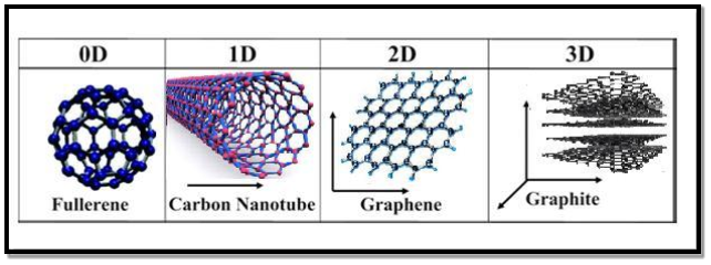
All materials are composed of grains. The visibility of grains depends on their size. Convectional materials have grains varying in size from hundreds of microns to millimetres. The materials processing grains size ranging from 1 to 100 nm, known as Nano materials. Nano materials can be produced in different dimensionalities.
- One dimensional nano material: Surface coatings and thin films
- Two dimensional nano materials: nano tubes nano wires, biopolymers
- Three dimensional nano materials: nano particles, precipitates, colloids, quantum dots, nano crystalline materials, fullerenes or carbon nano-60.
BOTTOM-UP AND TOP-DOWN APPROACH TO SYNTHESIS OF NANOMATERIALS
The synthesis of nanomaterials is key to the future success of this new technology. The methods of producing nanoparticles are classified into two main categories:
- Bottom-up approach
- Top-down approach
- Bottom up Approach
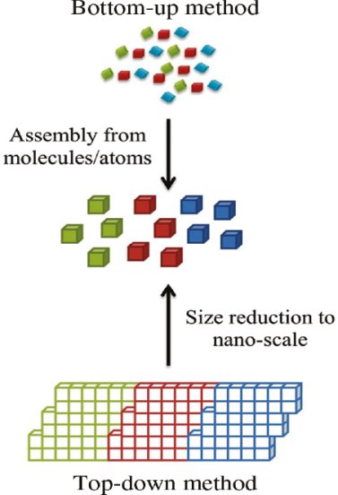
In bottom-up approaches nanomaterials are assembled from basic building blocks, such as molecules or nanoclusters. The basic building blocks, in general, are nanoscale objects with suitable properties that can be grown from elemental precursors. The concept of the bottom-up approach is that the complexity of nanoscale components should reside in their self-assembled internal structure, requiring as little intervention as possible in their fabrication from the macroscopic world.
The bottom-up approach uses atomic or molecular feed-stocks as the source of the material to be chemically transformed into larger nanoparticles. This has the advantage of being potentially much more convenient than the top down approach. By controlling the chemical reactions and the environment of the growing nanoparticle, then the size, shape and composition of the nanoparticles may all be affected. For this reason nanoparticles produced by bottom up, chemically based and designed, reactions are normally seen as being of higher quality and having greater potential applications. This has led to the growth of a host of common bottom up strategies for the synthesis of nanoparticles. Many of these techniques can be tailored to be performed in gas, liquid, solid states, hence the applicability of bottom-up strategies to a wide range of end products. Most of the bottom up strategies requires suitable organometallic complexes or metal salts to be used as chemical precursors, which are decomposed in a controlled manner resulting in particle nucleation and growth. One of the key differences that can be used to subdivide these strategies into different categories is the method by which the precursor is decomposed.
A typical example of bottom-up is processing for nanocomposite magnets from individual high-magnetization and high-coercivity nanoparticles. The assembling critically depends on availability of anisotropic (single crystal) hard magnetic nanoparticles. Anisotropic nanoparticles produced via surfactant-assisted high energy ball milling satisfy the major requirements for this application.
- Top down Approach
In top-down approaches, a bulk material is restructured (i.e. partially dismantled, machined, processed or deposited) to form nanomaterials. The aggressive scaling of electronic integrated circuits in recent years can be considered the greatest success of this paradigm. For top-down methods, the challenges increase as devices size is reduced and as the desired component designs become larger and more complex. Also the top-down assembly of nanocomponents over large areas is difficult and expensive.
The top-down method involves the systematic breakdown of a bulk material into smaller units using some form of grinding mechanism. This is beneficial and simple to execute and avoids the use of volatile and poisonous compounds frequently found in the bottom-up techniques. However, the quality of the nanoparticles formed by grinding is accepted to be poor in comparison with the material produced by modern bottom up methods. The main drawbacks include defect problems from grinding equipment, low particle surface areas, asymmetrical shape and size distributions and high energy needed to produce relatively small particles. Apart from these disadvantages, it must be distinguished that the nano-material produced from grinding still finds use, due to the simplicity of its manufacture, in applications including magnetic, catalytic and structural properties.
Nanomaterials behave differently as the size changes with respect to the bulk. It is necessary to characterize physical, structural and optical properties of a material to qualify as nanomaterial. Various characterization techniques are used to know the characteristics of the nanomaterials.
We will discuss the two techniques in this section.
- XRD Technique
- SEM (Scanning Electron Microscope) Technique
X-ray diffraction (XRD)
XRD is one of the most extensively used techniques for the characterization of nanoparticles. XRD provides information regarding the crystalline structure, nature of the phase, lattice parameters and crystalline grain size.
X-ray powder diffraction (XRD) is a rapid analytical technique primarily used for phase identification of a crystalline material and can provide information on unit cell dimensions. The analysed material is finely ground, homogenized, and average bulk composition is determined.
Powder X-ray diffraction has become a cornerstone technique for deriving crystallite size in nanoscience due to speed and "simplicity". An advantage of the XRD techniques commonly performed in samples of powder form, usually after drying their corresponding colloidal solutions, is that it results in statistically representative, volume-averaged values. The composition of the particles can be determined by comparing the position and intensity of the peaks. However, it is not suitable for amorphous materials and the XRD peaks are too broad for particles with a size below 3 nm.
Unfortunately, this apparently simple technique commonly has unexpected problems. Anisotropic peak broadening related to crystallite shape, defects, and microstrain occurs frequently in nanomaterials and can significantly complicate the analysis. In some instances, the usage of the conventional single peak approach would give erroneous results, and in others, this type of analysis is not even possible. A number of different nanocrystalline oxides have been examined to determine their crystallite sizes by different techniques. They differ in terms of crystal symmetry, crystallinity, density, and present different challenges with regard to size analysis.
Principle: X-ray diffraction is based on constructive interference of monochromatic X-rays and a crystalline sample. These X-rays are generated by a cathode ray tube, filtered to produce monochromatic radiation, collimated to concentrate, and directed toward the sample
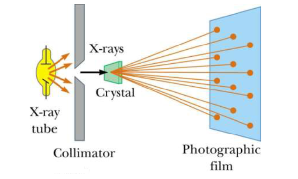
X-ray Diffraction (XRD) is one of the classical methods for identification and characterization of crystalline solids. Each crystalline solid has its unique characteristic X-ray powder pattern which issued as a ”fingerprint” for its identification. The method is based on the diffraction of X-rays by the sample in different directions. Waves of wavelength comparable to the crystal lattice spacing are strongly scattered (diffracted).
A powder X-ray diffractometer consists of an X-ray source (usually an X-ray tube), a sample stage, a detector and a way to vary angle θ. The X-ray is focused on the sample at some angle θ, while the detector opposite the source reads the intensity of the X-ray it receives at 2θ away from the source path. The incident angle is than increased over time while the detector angle always remains 2θ.
X-rays incident upon a crystal is scattered in different ways. When the wavelength of the radiation (λ) is comparable to the atomic spacing in a crystal, the scattering which is termed as diffraction, gives rise to a set of well-defined beams arranged with a characteristic geometry, thus forming a diffraction pattern. Schematic of X-ray diffraction setup is shown in figure.
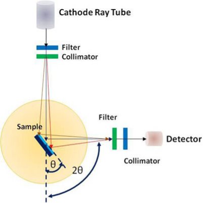
Figure: XRD Technique
X-ray diffraction data collection is the result of relative intensity (I) for each reflection with a set of planes in the crystal, designated by Miller indices (h k l), along with the corresponding scattering angle (2θ) for that reflection. The positions and intensities of the diffracted beams are a function of the arrangements of the atoms in space and some other atomic properties.
Thus, if the positions and the intensities of the diffracted beams are recorded, it is possible to deduce the arrangement of the atoms in the crystal and their chemical nature. A beam of radiation will only be diffracted when it imposed upon a set of planes in a crystal if the geometry of the situation fulfils quite specific law defined by Bragg’s known as Bragg’s law.
nλ =2dhkl sinθ
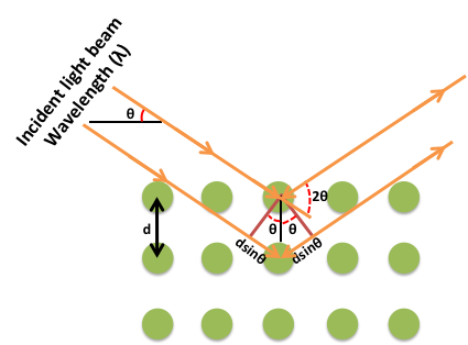
Figure: Bragg’s Law
The above equation is known as the Bragg equation, where n denotes the order of diffraction, λ represents the wavelength, d is the interplanar spacing of hkl planes in crystal lattice and θ signifies the Bragg angle.
A typical diffraction pattern shows the intensity Vs 2θ plot. Each peak corresponds to a specific (h k l) plane of the sample. The broadening of the diffraction peaks is due to two factors:
1) Due to size of crystallite
2) Due to micro strain of crystallite
Advantages
- It is a rapid and powerful technique for identifying unknown minerals and materials
- It only requires preparation of a minimal sample for analysis
- Interpreting the resulting data is relatively straightforward
- XRD measurement instruments are widely available
Disadvantages
- To best identify an unknown powder material, the sample should be homogeneous.
- Typically XRD analysis requires access to standard reference data.
- Preparation of samples often requires grinding them down to a powder
- If the crystal sample is non-isometric, then the indexing of patterns can be complex when determining unit cells
SCANNING ELECTRON MICROSCOPY (SEM)
The high resolution scanning electron microscope is a versatile tool for nanotechnology and advanced materials science, moreover, opens up new dimensions in archaeology, biology, earth science, meteorite research, hydrology and many other research areas.
Principle
In this technique, an electron beam is focused onto sample surface kept in a vacuum by electro-magnetic lenses (since electron possesses dual nature with properties of both particle and wave, hence an electron beam can be focused or condensed like an ordinary light). The beam is then scanned over the surface of the sample. The scattered electron from the sample is then fed to the detector and then to a cathode ray tube through an amplifier, where the images are formed, which gives the information of the sample
Instrumentation
It comprises of a heated filament as a source of electron beam, condenser lenses, aperture, evacuated chamber for placing the sample, electron detector, amplifier, CRT with image forming electronics, etc. The SEM is an instrument that produces a largely magnified image by using electrons instead of light to form an image. A schematic diagram of the SEM is shown in Figure. A beam of electrons is produced at the top of the microscope by an electron gun. The electron beam follows a vertical path through the microscope, which is held within a vacuum chamber.
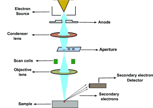
The beam travels through electromagnetic fields and lenses, which focus the beam down towards the sample. Once the beam hits the sample, electrons and X - rays are ejected from the sample. Detectors collect these X - rays, backscattered electrons and secondary electrons and convert them into a signal that is sent to a screen similar to a television screen. This produces the final image. In this research work, the powder samples were placed on the carbon tape which is attached to the sample holder.
The image formation in a scanning electron microscope is different from that in a conventional optical microscope. In SEM a focused mono-energetic electron beam scans the sample surface producing various "products" from the surface. These are secondary electrons, backscattered electrons and X-ray photons.
Advantages
- Advantages of a Scanning Electron Microscope include its wide-array of applications, the detailed three-dimensional and topographical imaging and the versatile information garnered from different detectors.
- SEMs are also easy to operate with the proper training and advances in computer technology and associated software make operation user-friendly.
- This instrument works fast, often completing SEI, BSE and EDS analyses in less than five minutes. In addition, the technological advances in modern SEMs allow for the generation of data in digital form.
- Although all samples must be prepared before placed in the vacuum chamber, most SEM samples require minimal preparation actions.
Disadvantages
- The disadvantages of a Scanning Electron Microscope start with the size and cost.
- SEMs are expensive, large and must be housed in an area free of any possible electric, magnetic or vibration interference.
- Maintenance involves keeping a steady voltage, currents to electromagnetic coils and circulation of cool water.
- Special training is required to operate an SEM as well as prepare samples.
- SEMs are limited to solid, inorganic samples small enough to fit inside the vacuum chamber that can handle moderate vacuum pressure.
- SEMs carry a small risk of radiation exposure associated with the electrons that scatter from beneath the sample surface.
Applications
- Scanning electron microscopy has been applied to the surface studies of metals, ceramics, polymers, composites and biological materials for both topography as well as compositional analysis.
- An extension of this technique is Electron Probe Micro Analysis (EPMA), where the emission of X-rays, from the sample surface, is studied upon exposure to a beam of high energy electrons.
- Depending on the type of detectors used this method is classified in to two as: Energy Dispersive Spectrometry (EDS) and Wavelength Dispersive Spectrometry (WDS). This technique is used extensively in the analysis of metallic and ceramic inclusions, inclusions in polymeric materials and diffusion profiles in electronic components.
Nanotubes
They are tubular structures with a hollow interior. There are nanotubes synthesized and characterized from inorganic laminar materials. However, the most studied are carbon nanotubes (CNT's).
Carbon nanotubes: Carbon nanotubes were first observed b Sunmino Iijima in 1911. Carbon exists in a large number of allotropic forms. These includes diamond, graphite and fullerenes (such as C60 , C70 etc.,). Carbon nanotubes are obtained by rolling the graphite sheet into tubes with the bonds at the ends of the sheet. These bonds are used to close the tube. Generally, the length of carbon nanotubes varies from several micrometres to millimetre and the diameter will vary from 1 to 20 nm.
A tube may contain one cylindrical wall of graphite or a number of concentric cylindrical walls. A carbon nanotube consisting of one cylindrical graphite is called single walled nanotube. Otherwise they are known as multi walled nanotubes.
Depending on how sheet is rolled, they are classified into three types. The three types of carbon nanotubes are 1) Zigzag 2) Chiral 3) Armchair
Properties of carbon nanotubes
Electrical conductivity: Generally the carbon nanotubes produced both in metallic and semiconducting in their electrical behaviour. Conductivity of multi walled nanotube id more complex. The conductivity and resistivity of ropes of single walled carbon nanotubes has been measured by placing the electrodes at different parts of the carbon nanotubes. The resistivity of single walled carbon nanotube ropes was of the order of 10-4 ohm-cm at 270. This means that the conductivity of single walled nanotube ropes are most conductive carbon fibres of known.
Magnetic property: The carbon nanotube displays the magneto-resistive effects at lower temperature i.e., the resistance of the carbon nanotube is changed by the application of dc magnetic field. The variation of resistance in carbon nanotube at 2.3K and 0.36k w.r.t magnetic field is observed. This show magneto- resistance effect is negative. This is due to the decrease in resistance with increase in magnetic field.
Highly absorbent: The carbon nanotubes have large surface area and high absorbance. So the carbon nanotubes are used in the air, gas and water filtration.
Mechanical properties: The strength of the sp2 carbon-carbon bonds gives carbon nanotubes amazing mechanical properties. The stiffness of the material is measured in terms of its Young’s modulus. The Young’s modulus value of single walled nanotube is about 1Tera Pascal, which is approximately 5 times greater than steel. The tensile strength or breaking strain of nanotube is about 150GPa, which is approximately 150 times greater than steel
Vibration properties: Similar to carbon dioxide molecule, Carbon nanotubes have two normal modes of vibration (a set of vibrational motions known as normal mode of vibrations). The different modes of vibrational motion are determined from the symmetry of the molecule. In the first mode the diameter of the carbon nanotube moves in and out at the frequency of 165 cm-1. In the second mode the carbon nanotube crushing in one direction and expansion takes place in the perpendicular direction. Thus, it oscillates between sphere and ellipse at a frequency of 17 cm-1. The frequency of the vibration modes depends on the diameter of the nanotube.
Nano materials possess unique and beneficial, physical, chemical and mechanical properties; they can be used for a wide verity of applications.
Material technology
- Nanocrystalline aerogel are light weight and porous, so they are used for insulation in offices homes, etc.
- Cutting tools made of Nano crystalline materials are much harder, much more wear- resistance, and last stranger.
- Nano crystalline material sensors are used for smoke detectors, ice detectors on air craft wings, etc.
- Nano crystalline materials are used for high energy density storage batteries.
- Nano sized titanium dioxide and zinc dioxide is used in sunscreens to absorb and reflect ultraviolet rays.
- Nano coating of highly activated titanium dioxide acts as water repellent and antibacterial.
- The hardness of metals can be predominately enhanced by using nanoparticles.
- Nanoparticles in paints change colour in response to change in temperature or chemical environment, and reduce the infrared absorption and heat loss.
- Nano crystalline ceramics are used in automotive industry as high strength springs, ball bearings and valve lifters.
Information technology
- Nanoscale fabricated magnetic materials are used in data storage
- Nanocomputer chips reduce the size of the computer.
- Nano crystalline starting light emitting phosphors are used for flat panel displays.
- Nanoparticles are used for information storage.
- Nanophotonic crystals are used in chemical optical computers.
Biomedical
- Biosensitive nanomaterials are used for ragging of DNA and DNA chips.
- In the medical field, nanomaterials are used for disease diagnosis, drug delivery and molecular imaging.
- Nano crystalline silicon carbide is used for artificial heart valves due to its low weight and high strength.
Energy storage
- Nanoparticles are used hydrogen storage.
- Nano particles are used in magnetic refrigeration.
- Metal nanoparticles are useful in fabrication of ionic batteries.
- Nano materials possess unique and beneficial, physical, chemical and mechanical properties; they can be used for a wide verity of applications.
Material technology
- Nanocrystalline aerogel are light weight and porous, so they are used for insulation in offices homes, etc.
- Cutting tools made of Nano crystalline materials are much harder, much more wear- resistance, and last stranger.
- Nano crystalline material sensors are used for smoke detectors, ice detectors on air craft wings, etc.
- Nano crystalline materials are used for high energy density storage batteries.
- Nano sized titanium dioxide and zinc dioxide is used in sunscreens to absorb and reflect ultraviolet rays.
- Nano coating of highly activated titanium dioxide acts as water repellent and antibacterial.
- The hardness of metals can be predominately enhanced by using nanoparticles.
- Nanoparticles in paints change colour in response to change in temperature or chemical environment, and reduce the infrared absorption and heat loss.
- Nano crystalline ceramics are used in automotive industry as high strength springs, ball bearings and valve lifters.
Information technology
- Nanoscale fabricated magnetic materials are used in data storage
- Nanocomputer chips reduce the size of the computer.
- Nano crystalline starting light emitting phosphors are used for flat panel displays.
- Nanoparticles are used for information storage.
- Nanophotonic crystals are used in chemical optical computers.
Biomedical
- Biosensitive nanomaterials are used for ragging of DNA and DNA chips.
- In the medical field, nanomaterials are used for disease diagnosis, drug delivery and molecular imaging.
- Nano crystalline silicon carbide is used for artificial heart valves due to its low weight and high strength.
Energy storage
- Nanoparticles are used hydrogen storage.
- Nano particles are used in magnetic refrigeration.
- Metal nanoparticles are useful in fabrication of ionic batteries.