UNIT 4
Semiconductor physics
Intrinsic semiconductor
Pure semiconductors are called intrinsic semiconductors.
Silicon and germanium are the most common examples of intrinsic semiconductors. Both these semiconductors are most frequently used in the manufacturing of transistors, diodes and other electronic components.
Intrinsic semiconductor is also called as undoped semiconductor or I-type semiconductor. In intrinsic semiconductor the number of electrons in the conduction band is equal to the number of holes in the valence band. Therefore, the overall electric charge of atom is neutral
The semiconductor in which impurities are added is called extrinsic semiconductor. When the impurities are added to the intrinsic semiconductor, it becomes an extrinsic semiconductor. The process of adding impurities to the semiconductor is called doping. Doping increases the electrical conductivity of a semiconductor.
Extrinsic semiconductor
Extrinsic semiconductor has higher electrical conductivity than intrinsic semiconductor. Hence the extrinsic semiconductors are used for the manufacturing of electronic devices such as diodes, transistors etc. The number of free electrons and holes in extrinsic semiconductors are not equal.
Types of impurities
Two types of impurities are added to the semiconductor. They are pentavalent and trivalent impurities.
Pentavalent impurities
Pentavalent impurity atoms have 5 valence electrons. The various examples of pentavalent impurity atoms include Phosphorus (P), Arsenic (As), Antimony (Sb), etc. The atomic structure of pentavalent atom (phosphorus) and trivalent atom (boron) is shown in below fig.
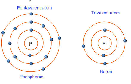
Phosphorus is a substance consisting of atoms which all have the same number of protons. The atomic number of phosphorus is 15 i.e. 15 protons. The number of protons in the nucleus of an atom is called atomic number. Phosphorus atom has 15 electrons (2 electrons in first orbit, 8 electrons in second orbit and 5 electrons in the outermost orbit).
Trivalent impurities
Trivalent impurity atoms have 3 valence electrons. The various examples of trivalent impurities include Boron (B), Gallium (G), Indium (In), Aluminium (Al).
Boron is a substance consisting of atoms which all have the same number of protons. The atomic number of boron is 5 i.e. 5 protons. Boron atom has 5 electrons (2 electrons in first orbit and 3 electrons in the outermost orbit).
Classification of extrinsic semiconductors based on impurities added
Based on the type of impurities added, extrinsic semiconductors are classified into two types.
N-type semiconductor
P-type semiconductor
Negative charge carriers (Electron)
The negative charge carriers such as free electrons are the charge carriers that carry negative charge with them while moving from one place to another place. Free electrons are the electrons that are detached from the parent atom and move freely from one place to another place.
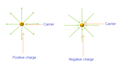
Positive charge carriers (Holes)
The positive charge carriers such as holes are the charge carriers that carry positive charge with them while moving from one place to another place. Holes are the vacancies in the valence band that moves from one place to another place within the valence band.
The charge carriers that are present in large quantities are called majority charge carriers. The majority charge carriers carry most of the electric charge or electric current in the semiconductor. Hence, majority charge carriers are mainly responsible for electric current flow in the semiconductor.
The charge carriers that are present in small quantities are called minority charge carriers. The minority charge carriers carry a very small amount of electric charge or electric current in the semiconductor.
Charge carriers in intrinsic semiconductor
The semiconductors that are in pure form are called intrinsic semiconductors. In intrinsic semiconductor the total number of negative charge carriers (free electrons) is equal to the total number of positive charge carriers (holes or vacancy).
Total negative charge carriers = Total positive charge carriers
The current is addition of two current , current  due to flow of holes and current
  due to flow of electron
So 
We will calculate conductivity due to flow electron only
E = electric field vector across the small section (in cylindrical form) of semiconductors
N= number of electron in above semiconductor
A= cross sectional area
L= length of section of cylindrical semiconductor
Let one electron contains charge q than total charge flow will be = Nq
So current flow due to electron will be
 = (Total charge flow)/ (time taken in flow of charge)
 =
= 
Time  = (Average distance covered by electron) / (drift velocity of electron)
 =
= 
From above equation
● = 
● Let conduction current density due to flow of current (due to flow of electron ) is  , and we know that
 =
= 
From above equation

= 
 =
= 
Where  =
=  = number of electrons per unit volume
Drift velocity of electron can be expressed as
 =
= 
Where  is mobility of electron
From Equation
 =
= 
From ohm's law we know that
 =
= 
Where  is conductivity due to flow of electron
By comparing equation, we can concluded that
 =
= 
Above equation gives the expression of conductivity of semiconductor due to flow of electrons
In similar fashion we can calculate conductivity of semiconductor due to flow of holes
Let  holes per unit volume flow in semiconductor, and
  is the mobility of hole
  is charge on hole,
So, conductivity expression due to holes can be given by
● = 
Total conductivity  of semiconductor (due to flow of electron as well as holes) can be given by
 =
=  +
+
=  +
+ 
 =
= 
For intrinsic semiconductor

Where  is the intrinsic carrier concentration per unit volume of intrinsic semiconductor
So conductivity of intrinsic semiconductor can be given by
 =
=  (
( )
)
Drift current
The flow of electric current due to the motion of charge carriers under the
The influence of an external electric field is called drift current.
When an electric field E is applied across a semiconductor material, the charge
Carriers attain a drift velocity vd.
So, drift velocity
Vd=µE----------------(1)
The relation between current density J and drift velocity vd is
J=Nqvd
Where N is the carrier concentration
q is the charge of electron or hole
From equations (1) and (2), we get

_ is the mobility of a charge carrier.
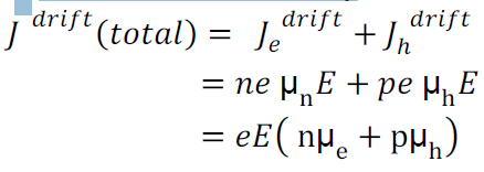
The above equation shows the general expression for drift current density.
Drift current density due to electrons is

Where is the electrons carrier concentration and
µe the mobility of electrons
Drift current density due to holes is

T Total drift current density:
Diffusion current:
The flow of electric current due to the motion of charge carriers under concentration
Gradient is called diffusion current
Or
The motion of charge carriers from the region of higher concentration to lower
Concentration leads to a current called diffusion current.
Let be the excess electron concentration. Then according to Fick’s law, the rate of
Diffusion of charge carriers is proportional to concentration gradient is

Hence
Rate of diffusion of charge:
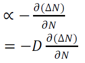
Where D is the diffusion coefficient of charge carriers
The negative sign indicates decrease of N with increase of x
So, the diffusion current density Jdiffu is:

The expression for total current density due to holes is

The expression for total current density due to electrons is

When a material carrying current is subjected to a magnetic field in a direction perpendicular to direction of current, an electric field is developed across the material in a direction perpendicular to both the direction of magnetic field and current direction. This phenomenon is called “Hall-effect”.
Explanation:
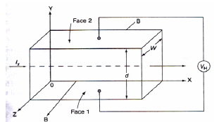
* Consider a semi-conductor, and current passes along the X-axis and a magnetic field Bz is applied along the Z-direction, a field Ey is called the Hall field which is developed in the Y-direction.
* In P- type semi-conductor, holes move with the velocity “V” in the “+”ve X-direction. As they move across the semiconductor the holes experience a transverse force ‘Bev’ due to the magnetic field.
* This force drives the holes down to the lower face. As a result, the lower face becomes +vely charged and –ve charge on the upper surface creating the hall field in the Y-direction. The Hall field exerts an upward force on holes equal to Ee.
* In the steady state, two forces just balance and as a result, no further increase of + ve charge occurs on Face1.
* In N type semiconductor, the majority charge carriers are electrons that experience a force in the downward direction and the lower face gets – vely charged. As a result, Hall field will be in the Y – direction.
Hall Coefficient:
Hall field𝐸𝐻, for a given material depends on the current density J and the applied magnetic field B.
i.e. 𝐸𝐻α JB
𝐸𝐻 = 𝑅𝐻 α JB
Since,
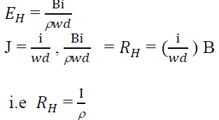
This is called hall coefficient.
When a layer of P - type semiconducting material is placed with a layer of N- type semiconducting material in such a way that the atoms of P-type combine with the atoms of N-type across the surface of contact, such a surface junction where combination has occurred is known as PN junction.
Combined p-type and n-type semiconductors with PN junction formation is known a junction diode or PN diode
Biased pn junction diode by diffusion technique:
Diffused junctions are formed by impurity diffusion technique. The diffusion process employs either gas diffusion method or solid diffusion method for example in gas diffusion method a wafer of n-type silicon is heated at about 10000 c in a gaseous atmosphere of high concentration gradient the boron atoms.
At the temperature due to concentration gradient the boron atom diffuses into silicon forming a p-n junction in solid diffusion process a p-type impurity (say indium) is painted on a n-type substrate and both are heated. Now impurity atoms diffuse into n-type substrate for a short distance and form a p-n junction.

*The formation PN junction is represented in a figure. Let us consider the formation of a sharp junction when two separate semiconductors of p and n type are brought together.
* The p-type has holes as majority carriers and electrons as minority carriers while n-type has electrons as majority carriers and holes as minority carriers.
* When they are joined, in the region of contact the free electrons diffuse from the n-region and combine with holes in the p-region. This leaves n-region near the boundary positively charged and p-region negatively as a result, electric field EB appears in a small region W on either side of the junction O. This region is called the “Depletion region “. The thickness of this region is in the older of 6 ×10⁻⁶ cm.
* Due to electric field E B potential difference appears across the depletion region and this potential VB is called “Contact Potential or Barrier Potential or Junction Barrier”.
Light Emitting Diodes (LEDs) are the most widely used semiconductor diodes among all the different types of semiconductor diodes available today. Light emitting diodes emit either visible light or invisible infrared light when forward biased. The LEDs which emit invisible infrared light are used for remote controls
When Light Emitting Diode (LED) is forward biased, free electrons in the conduction band recombines with the holes in the valence band and release energy in the form of light.
The process of emitting light in response to the strong electric field or flow of electric current is called electroluminescence.
A normal p-n junction diode allows electric current only in one direction. It allows electric current when forward biased and does not allow electric current when reverse biased. Thus, a normal p-n junction diode operates only in forward bias condition.
Light Emitting Diode (LED) works only in forward bias condition. When Light Emitting Diode (LED) is forward biased, the free electrons from n-side and the holes from p-side are pushed towards the junction.
When free electrons reach the junction or depletion region, some of the free electrons recombine with the holes in the positive ions. We know that positive ions have less number of electrons than protons. Therefore, they are ready to accept electrons. Thus, free electrons recombine with holes in the depletion region. In the similar way, holes from p-side recombine with electrons in the depletion region.
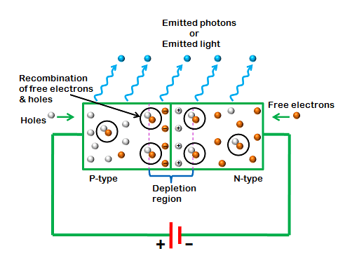
Because of the recombination of free electrons and holes in the depletion region, the width of depletion region decreases. As a result, more charge carriers will cross the p-n junction.
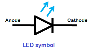
The symbol of LED is similar to the normal p-n junction diode except that it contains arrows pointing away from the diode indicating that light is being emitted by the diode.
Merits:
1. Very low voltage and current are enough to drive the LED.
Voltage range – 1 to 2 volts. Current – 5 to 20 milliamperes.
2. Total power output will be less than 150 milliwatts.
3. The response time is very less – only about 10 nanoseconds.
4. The device does not need any heating and warm up time.
5. Miniature in size and hence lightweight.
6. Have a rugged construction and hence can withstand shock and vibrations.
7. An LED has a lifespan of more than 20 years.
Demerits:
1. A slight excess of voltage or current can damage the device.
2. The device is known to have a much wider bandwidth compared to the laser.
3. The temperature depends on the radiant output power and wavelength.
It is a form of light-weight sensor that converts light energy into electrical voltage or current. Photodiode is a type of semiconducting device with PN junction. Between the p (positive) and n (negative) layers, an intrinsic layer is present. The photo diode accepts light energy as input to generate electric current.
Typical photodiode materials are Silicon, Germanium, Indium Gallium Arsenide Phosphide and Indium gallium arsenide.
Internally, a photodiode has optical filters, built in lens and a surface area. When the surface area of photodiodes increases, it results in more response time. Few photo diodes will look like Light Emitting Diodes (LED). It has two terminals . The smaller terminal acts as cathode and the longer terminal acts as anode.
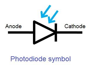
The symbol of the photodiode is similar to that of an LED but the arrows point inwards as opposed to outwards in the LED. The following image shows the symbol of a photodiode.
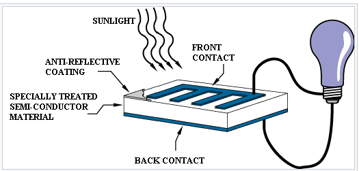
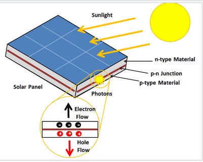
A solar panel works by allowing photons, or particles of light, to knock electrons free from atoms, generating a flow of electricity. Solar panels actually comprise many, smaller units called photovoltaic cells. (Photovoltaic simply means they convert sunlight into electricity.) Many cells linked together make up a solar panel
Photovoltaic cells, through the photovoltaic effect, absorb sunlight and generate flowing electricity. This process varies depending on the type of solar technology, but there are a few steps common across all solar photovoltaic cells.
Step 1: Light is absorbed by the PV cell and knocks electrons loose
First, light strikes a photovoltaic cell and is absorbed by the semiconducting material it is made from (usually silicon). This incoming light energy causes electrons in the silicon to be knocked loose, which will eventually become the solar electricity you can use in your home.
Step 2: Electrons begin to flow, creating an electrical current
There are two layers of silicon used in photovoltaic cells, and each one is specially treated, or “doped”, to create an electric field, meaning one side has a net positive charge and one has a net negative charge. This electric field causes loose electrons to flow in one direction through the solar cell, generating an electrical current.
Step 3: The electrical current is captured and combined with other solar cells
Once an electrical current is generated by loose electrons, metal plates on the sides of each solar cell collect those electrons and transfer them to wires. At this point, electrons can flow as electricity through the wiring to a solar inverter and then throughout your home.
