Module 2
Interfacing of 8085
2. 1 Interfacing of 8085 with 8255, 8254/8253, 8251, 8259
Step 1:
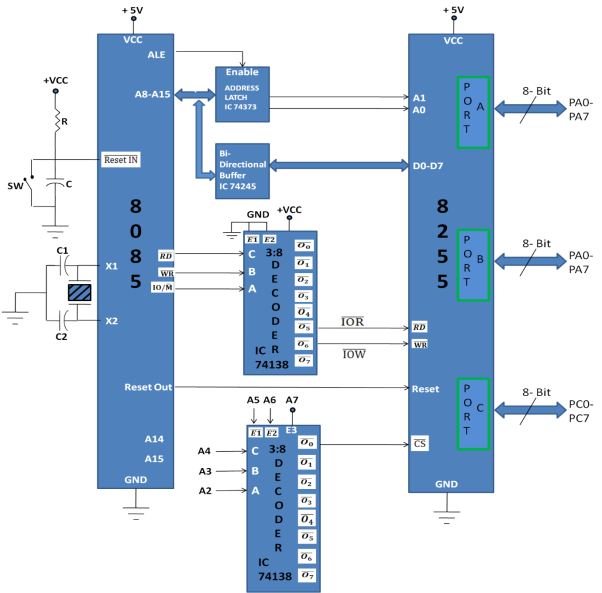
A0-A7 is the Lower- order of 8-bit address separated from AD0-AD7 using address latch/buffer for example IC 74373 and ALE signal.
The separated address lines A0-A7 are connected to A0-A7 input pins of 8255 and the separated data bus D0-D7 are connected to D0-D7 pins of 8255.
Reset out of 8085 is connected to reset pin of 8255.
Step 2:
8255 does not have internal separate control logic generator, hence the IO/ ,
,  and
and  control signals are not connected directly to 8255. These pins are given first to decoder and decoded using 3:8 decoder
For example: IC 74138.
The generated control signals  and
and  are connected to
  and
and  input of 8255.
Step 3:
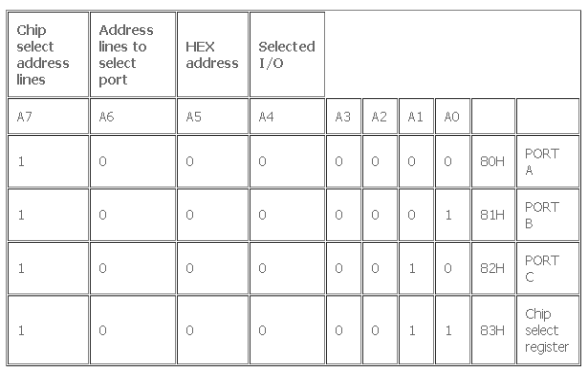
An active low signal of chip select logic is obtained decoding remaining address lines of lower order addresses A2- A7.
Chip select logic and IO port address for this interfacing circuit are as:
Interfacing Diagram
Interfacing of 8255 with 8253/8254
The 8253/54 solves one of most common problem in any microcomputer system, the generation of accurate time delays under software control. Instead of setting up timing loops in system software, the programmer configures the 8253/54 to match his requirements, initializes one of the counters of the 8253/54 with the desired quantity, then upon command the 8253/54 will count out the delay and interrupt the CPU when it has completed its task.
Functional Diagram of 8253/8254:
It includes three counters, a data bus buffer, Read/Write control logic, and a control register.
Each counter has two input signals CLOCK and GATE and one output signal OUT.
Data Bus Buffer:
This tri-state, bi-directional, 8-bit buffer is used to interface the 8253/54 to the system data bus.
The Data bus buffer has three basic functions.
1. Programming the modes of 8253/54.
2. Loading the count registers.
3. Reading the count values.
Read/Write Logic:
The Read/Write logic has five signals:
RD, WR, CS and the address lines A0 and A1.
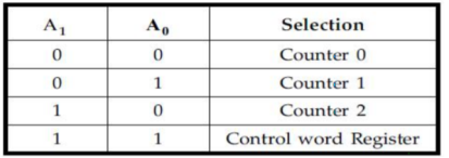
The control word register and counters are selected according to the signals on lines A0 and A1.
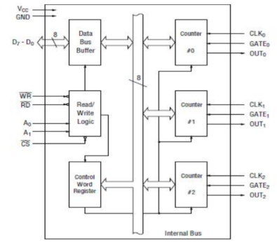
Block Diagram of 8253
Control Word Register:
This register is accessed when lines A0 and A1 are at logic 1. It is used to write a command word which specifies the counter to be used (binary or BCD), its mode, and either a read or write operation.
Counters:
Each counter consists of a single 16- bit pre-settable, down counter. The counter can operate in either binary or BCD its input, gate and output are configured by the selection of modes stored in the control word register.
The programmer can read the contents of any of the three counters without disturbing the actual count in process.
Each counter has program control word which is used to select the counter operation. If two bytes are programmed, then the first byte (LSB) stops the count, and the second byte (MSB) starts the counter with the new count.
GATE:
The gate input controls the operation of the counter in some modes.
OUT:
A counter output is the waveform generated by the timer.
RD/WR: Read/Write
This causes the data to be read/written from the 8254 and often connects to the
IORC/IOWC.
Operational Description:
The functional definition of the 8253/54 is programmed by the system software. Once programmed, the 8253/54 is ready to perform whatever timing tasks it is assigned to accomplish.
Programming the 8253/54:
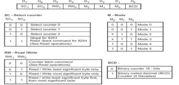
Each counter of the 8253/54 is programmed individually by writing a control word into the control word register (A0 - A1 = 11).
The Figure shows the control word format.
Bits SC1 and SC0 select the counter, bits RW1 and RW0 select the read, write or latch command, bits M2, M1 and M0 select the mode of operation and bit BCD decides whether it is a BCD counter or binary counter.
WRITE Operation:
1. Write a control word into control register.
2. Load the low-order byte of a count in the counter register.
3. Load the high-order byte of count in the counter register.
READ Operation:
In some applications, especially in event counters, it is necessary to read the value of the count in process. This is done by three possible methods:
1. Simple Read: It involves reading a count after inhibiting the counter by controlling the gate input or the clock input of the selected counter, and two I/O read operations are performed by the CPU. The first I/O operation reads the low-order byte, and the second I/O operation reads the high order byte.
2. Counter Latch Command: In this method, an appropriate control word is written into the control register to latch a count in the output latch, and two I/O read operations are performed by the CPU. The first I/O operation reads the low-order byte, and the second I/O operation reads the high order byte.
3. Read-Back Command (Available only for 8254): The third method uses the Read-Back command. This command allows the user to check the count value, programmed Mode, and current status of the OUT pin and Null count flag of the selected counter(s).
Interfacing of 8255 with 8251
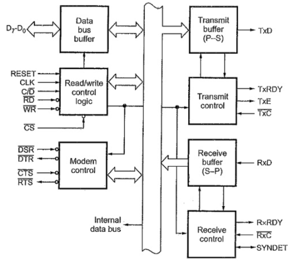
Data Bus Buffer :
This tri-state, bi-directional, 8-bit buffer is used to interface 8251 to the system data bus. Along with the data, control word, command words and status information are transferred through the Data Bus Buffer.
Read/Write control logic :
This functional block accepts inputs from the system, control bus and generate control signals for overall device operation.
It decodes control signals on 8085 control bus into signals which controls the internal and external I/O bus. It contains control word register and command word register that stores the various control formats for the device to function.
Transmit Buffer:
The transmit buffer accepts parallel data from the CPU, adds the appropriate framing information, serializes it, and transmits it on the TxD pin on the falling edge of TxC.
It consists of two registers the buffer register to hold eight bits and an output register to convert eight bits into a stream of serial bits.
The CPU writes a byte in the buffer register which is transferred to the output register when it is empty. The output register then transmits serial data on the TxD pin.
In asynchronous mode the transmitter adds START bit depending on how the unit is programmed also adds an optional even or odd parity bit, and either 1, 1 1/2, or 2 STOP bits.
In synchronous mode no extra bits are generated by the transmitter.
8251 Transmitter Control:
TxRDY (Transmit Ready ) : This output signal indicates CPU that buffer register is empty and the USART is ready to accept a data character. It can be used as an interrupt to the system for polled operation, the CPU can ‘check TxRDY using the status read operation. This signal is reset when a data byte is loaded into the buffer register.
TxE (Transmitter Empty) : This is an output signal. A high on this line indicates that the output buffer is empty. In synchronous mode, if the CPU has failed to load a new character in time, TxE will go high momentarily as SYN characters are loaded into the transmitter to fill the gap in transmission.
TxC (Transmitter Clock) : This clock controls the rate at which characters are transmitted by USART. In the synchronous mode TxC is equivalent to the ‘baud rate, and supplied by the modem.
In asynchronous mode TxC is 1, 16, or 64 times the baud rate. The clock division is programmable. It can be programmed by writing proper mode word in the mode set register.
Receiver Buffer:
The receiver accepts serial data on the RxD line, converts this serial data to parallel format, checks for bits or characters that are unique to the communication technique and sends an “assembled” character to the CPU.
In asynchronous mode it is ready to accept a character, it looks for a low level on the RxD line. On receiving the low level, it assumes that it is a START bit and enables an internal counter, At a count equivalent to one-half of a hit time, the RxD line is sampled again.
If the line is still low then valid START bit is detected and the 8251A proceeds to assemble the character. After successful reception of a START bit the 8251A receives data, parity and STOP bits, and transfers the data on the receiver input register. The data is then transferred into the receiver buffer register.
In the synchronous mode the receiver simply receives the specified number of data bits and transfers them to the receiver input register and then to the receiver buffer register.
Receiver Control:
It manages all receiver-related activities. It detects false start bit detection, parity error detection, framing error detection, sync detection and break detection.
RxRDY (Receiver Ready): This is an output signal. It goes high when the USART has a character in the buffer register and is ready to transfer to CPU.
This line is used either to indicate the status in the status register or to interrupt the CPU. This signal is reset when a data byte from receiver buffer is read by the CPU.
RxC (Receiver Clock): This clock controls the rate at which the character is to be received by USART in the synchronous mode. RxC is equivalent to baud rate which is supplied by the modem.
In asynchronous mode RxC is 1, 16, or 64 times the baud rate. The clock division is programmable. It can be programmed by writing proper mode word in the mode set register.
Modem Control:
The 8251 Block Diagram in Microprocessor has a set of control inputs and output’s which is used to simplify the interface to almost any modem.
It provides control circuitry for the generation of RTS and DTR and the reception of CTS and DSR.
The general- purpose inverted output and a general purpose input are provided.
The output is labelled DTR and the input is labelled DSR.
DTR can be asserted by setting bit 2 of the command instruction.
DSR can be sensed as bit 7 of the status register.
When used as a modem control signal DTR indicates that the terminal is ready to communicate and DSR indicates that it is ready for communication.
Control Word of 8251:
The Control Word of 8251 defines the complete functional definition of 8251 which must be loaded before any transmission or reception.
The control words are split into two formats
- Mode instruction
- Command instruction
Mode Instruction: The figure shows the mode instruction format of 8251.
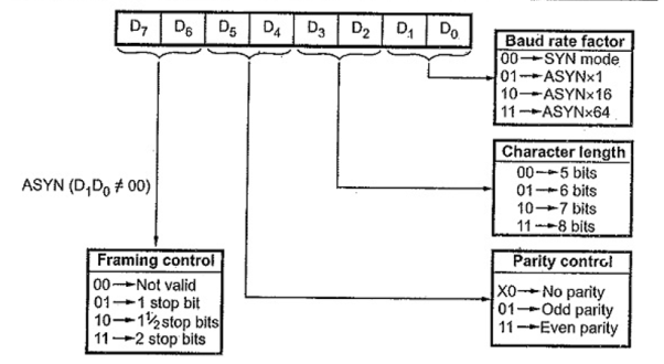
Mode instruction format
The instruction is considered as four 2-bit fields.
The first 2-bit field (D1-D0) determines whether USART has to operate in synchronous (00) or asynchronous mode.
In asynchronous mode it determines the division factor for clock to decide the baud rate.
For example, if D1 and D0 are both ones, then RxC and TxC will be divided by 64 to establish the baud rate.
The second 2-bit field (D3-D2) determine the number of data bits in one character. With this 2-bit field we can set character length from 5-bits to 8 bits.
The third 2-bit field, (D5-D4) controls parity generation. The parity bit is added to the data bits only if parity is enabled.
The last field, (D7-D6), has two meanings depending on whether operation has to be in synchronous or asynchronous mode.
For asynchronous mode, (i.e. D1D0 ≠ 00), it controls the number of STOP bits to be transmitted with the character.
In synchronous mode, (i.e. D1D0) = 00) this field controls the synchronizing process. It decides whether to operate with external synchronization or internal synchronization and whether to transmit single synchronizing character or two synchronizing characters.
Command Instruction:
After mode instruction, command character is issued to USART. It controls the operation of the USART within the basic framework established by the mode instruction. Figure shows command instruction format.
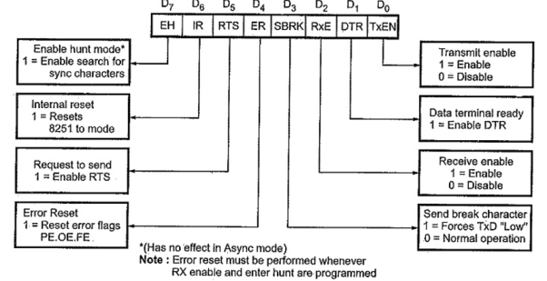
It does function such as: Enable Transmit/Receive; Error Reset and modem Control.
8251A Status Word:
It is necessary to check the “status” of transmitter and receiver for communication purposes. It is also necessary for CPU to know if any error has occurred during communication.
The 8251 Block Diagram in Microprocessor allow the programmer to read above mentioned information from the status register any time during the functional operation.
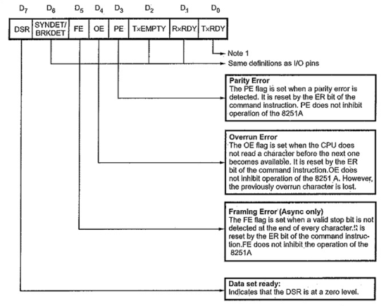
Status register format
Interfacing of 8255 with 8259
Features:
- Intel 8259 is designed for Intel 8085 and 8086 microprocessors.
- Can be programmed either in level triggered or in edge triggered interrupt level.
- The individual bits of interrupt request register can be masked.
- The interrupt handling capability can be increased up to 64 interrupt level by cascading further 8259 PIC.
- Clock cycle is not required.
Pin Diagram of 8259 –
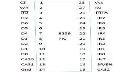
A total 28 pins in 8259 PIC microprocessor where
Vcc :5V Power supply and
Gnd: ground.
Block Diagram of 8259 PIC microprocessor –
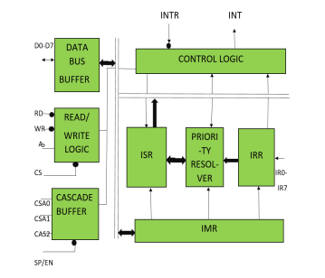
The Block Diagram consists of 8 blocks which are – Data Bus Buffer, Read/Write Logic, Cascade Buffer Comparator, Control Logic, Priority Resolver and 3 registers- ISR, IRR, IMR.
- Data bus buffer –
This is used as mediator between 8259 and 8085/8086 microprocessor by acting as a buffer.
It takes the control word from the 8085 microprocessor and transfer it to the control logic of 8259 microprocessor.
After selection of Interrupt 8259 microprocessor transfer the opcode of the selected Interrupt and address of the Interrupt service sub routine to the other connected microprocessor.
The data bus buffer consists of 8 bits represented as D0-D7 in the block diagram. A maximum of 8 bits data can be transferred at a time.
2. Read/Write logic –
This block works only when the value of pin CS is low (as this pin is active low). This block is responsible for the flow of data depending upon the inputs of RD and WR. These two pins are active low pins used for read and write operations.
3. Control logic –
It is the centre of the microprocessor and controls the functioning of every block. It has pin INTR which is connected with other microprocessor for taking interrupt request and pin INT for giving the output. If 8259 is enabled, and the other microprocessor Interrupt flag is high then this causes the value of the output INT pin high and in this way 8259 responds to the request made by another microprocessor.
4. Interrupt request register (IRR) –
It stores all the interrupt level requesting for Interrupt services.
5. Interrupt service register (ISR) –
It stores the interrupt level which are currently being executed.
6. Interrupt mask register (IMR) –
It stores the interrupt level which must be masked by storing the masking bits of the interrupt level.
7. Priority resolver –
It examines all the three registers and set the priority of interrupts and according to the priority of the interrupts, interrupt with highest priority is set in ISR register. Also, it reset the interrupt level which is already been serviced in IRR.
8. Cascade buffer –
To increase the Interrupt handling capability, we can cascade more number of pins with the help of using cascade buffer. So, during increment of interrupt capability, CSA lines are used to control multiple interrupt structure.
PPI 8255 is a general purpose programmable I/O device designed to interface the CPU with its outside world such as ADC, DAC, keyboard etc. We can program it according to the given condition. It can be used with almost any microprocessor.
It consists of three 8-bit bidirectional I/O ports i.e. PORT A, PORT B and PORT C. We can assign different ports as input or output functions.
Block diagram –
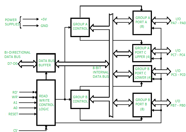
It consists of 40 pins and operates in +5V regulated power supply. Port C is further divided into two 4-bit ports i.e. port C lower and port C upper and port C can work in either BSR (bit set rest) mode or in mode 0 of input-output mode of 8255. Port B can work in either mode or in mode 1 of input-output mode. Port A can work either in mode 0, mode 1 or mode 2 of input-output mode.
It has two control groups, control group A and control group B. Control group A consist of port A and port C upper. Control group B consists of port C lower and port B.
Depending upon the value if CS’, A1 and A0 we can select different ports in different modes as input-output function or BSR. This is done by writing a suitable word in control register (control word D0-D7).
CS’ | A1 | A0 | SELECTION | ADDRESS |
0 | 0 | 0 | PORT A | 80 H |
0 | 0 | 1 | PORT B | 81 H |
0 | 1 | 0 | PORT C | 82 H |
0 | 1 | 1 | Control Register | 83 H |
1 | X | X | No Seletion | X |
Pin diagram –
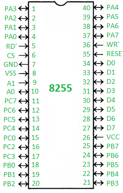
- PA0 – PA7 – Pins of port A
- PB0 – PB7 – Pins of port B
- PC0 – PC7 – Pins of port C
- D0 – D7 – Data pins for the transfer of data
- RESET – Reset input
- RD’ – Read input
- WR’ – Write input
- CS’ – Chip select
- A1 and A0 – Address pins
Operating modes –
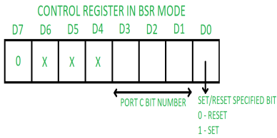
- Bit set reset (BSR) mode –
If MSB of control word (D7) is 0, PPI works in BSR mode. In this mode only port C bits are used for set or reset.
2. Input-Output mode –
If MSB of control word (D7) is 1, PPI works in input-output mode. This is further divided into three modes:
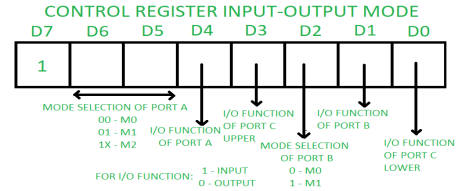
- Mode 0 –In this mode all the three ports (port A, B, C) can work as simple input function or simple output function. In this mode there is no interrupt handling capacity.
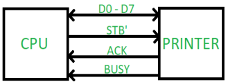
- Mode 1 – Handshake I/O mode or strobbed I/O mode. In this mode either port A or port B can work as simple input port or simple output port, and port C bits are used for handshake signals before actual data transmission. It has interrupt handling capacity and input and output are latched.
Example: A CPU wants to transfer data to a printer. In this case since speed of processor is very fast as compared to relatively slow printer, so before actual data transfer it will send handshake signals to the printer for synchronization of the speed of the CPU and the peripherals.
- Mode 2 – Bi-directional data bus mode. In this mode only port A works, and port B can work either in mode 0 or mode 1. 6 bits port C are used as handshake signals. It also has interrupt handling capacity.
- Figure shows the internal block diagram of 8255A. It consists of data bus buffer, control logic and Group A and Group B controls.
- Data Bus Buffer: This tri-state bi-directional buffer is used to interface the internal data lilts of 8255 to the system data bus. Input or Output instructions executed by the CPU either Read date from or Write data into the buffer. Output data from the CPU to the ports or control register, and input data to the CPU from the ports or status register are all passed through the buffer.
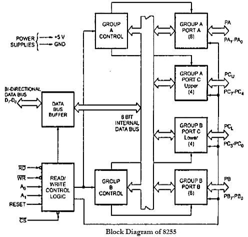
- Control Logic: The control logic block accepts control bus signals as well as inputs from the address bus, and issues commands to the individual group control blocks (Group A control and Group B control). It issues appropriate enabling signals to access the required data/control words or status word. The input pins for the control logic section are described here.
- Group A and Group B Controls: Each of the Group A and Group B control blocks receives control words from the CPU and issues appropriate commands to the ports associated with it. The Group A control block controls Port A and PC_7-PC_4 while the Group B control block controls Port B and PC_3-PC_0.
- Port A: This has an 8-bit latched and buffered output and an 8-bit input latch. It can be programmed in three modes: mode 0, mode 1 and mode 2.
- Port B: This has an 8-bit data I/O latch/ buffer and an 8-bit data input buffer. It can be programmed in mode 0 and mode 1.
- Port C: This has one 8-bit unlatched input buffer and an 8-bit output latch/buffer. Port C can be spitted into two parts and each can be used as control signals for ports A and B in the handshake mode. It can be programmed for bit set/reset operation.
The PIO 8255 is used for interfacing the analog to digital converters with microprocessor.
• The analog to digital converters is treaded as an input device by the microprocessor, that sends an initialising signal to the ADC to start the analog to digital data conversation process.
The process of analog to digital conversion is a slow process, and the microprocessor has to wait for the digital data till the conversion is over.
After the conversion is over, the ADC sends end of conversion EOC signal to inform the microprocessor that the conversion is over and the result is ready at the output buffer of the ADC.
These tasks of issuing an SOC pulse to ADC, reading EOC signal from the ADC and reading the digital output of the ADC are carried out by the CPU using 8255 I/O ports.
The time taken by the ADC from the active edge of SOC pulse till the active edge of EOC signal is called as the conversion delay of the ADC.
General algorithm for ADC interfacing contains the following steps:
1. Ensure the stability of analog input, applied to the ADC.
2. Issue start of conversion pulse to ADC
3. Read end of conversion signal to mark the end of conversion processes.
4. Read digital data output of the ADC as equivalent digital output.
• Analog input voltage must be constant at the input of the ADC right from the start of conversion till the end of the conversion to get correct results. This may be ensured by a sample and hold circuit which samples the analog signal and holds it constant for a specific time duration. The microprocessor may issue a hold signal to the sample and hold circuit.
• If the applied input changes before the complete conversion process is over, the digital equivalent of the analog input calculated by the ADC may not be correct.
• The analog to digital converter chips 0808 and 0809 are 8- bit CMOS, successive approximation converters. This technique is one of the fast techniques for analog to digital conversion.
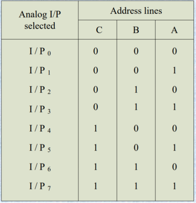
These converters internally have a 3:8 analog multiplexer so that at a time eight different analog conversion by using address lines ADD A, ADD B, ADD C.
Using these address inputs, multichannel data acquisition system can be designed using a single ADC.
The CPU may drive these lines using output port lines in case of multichannel applications. In case of single input applications, these may be hardwired to select the proper input.
There are unipolar analog to digital converters, that can convert only positive analog input voltage to their digital equivalent. These chips don’t contain any internal sample and hold circuit.
If one needs a sample and hold circuit for the conversion of fast signal into equivalent digital quantities, it has to be externally connected at each of the analog inputs.
Vcc Supply pins +5V
• GND GND
• Vref + Reference voltage positive +5 Volts maximum.
• Vref _ Reference voltage negative 0 Volts minimum.
- I/P 0 –I/P 7 Analog inputs
• ADD A,B,C Address lines for selecting analog inputs.
• O 7 – O 0 Digital 8-bit output with O 7 MSB and O 0 LSB
• SOC Start of conversion signal pin
• EOC End of conversion signal pin
• OE Output latch enable pin, if high enables output
• CLK Clock input for ADC
- A typical Hexa keyboard and 7-segment LED display interfacing circuit using 8279 is shown.
- The circuit can be used in 8085 microprocessor system and consist of 16 numbers of hexa-keys and 6 numbers of 7-segment LEDs.
- The 7-segment LEDs can be used to display six digit alphanumeric character.
- The 8279 can be memory mapped or I/O mapped in the system. In the circuit shown is the 8279 is I/O mapped.
- The address line A0 of the system is used as A0 of 8279.
- The clock signal for 8279 is obtained by dividing the output clock signal of 8085 by a clock divider circuit.
- The chip select signal is obtained from the I/O address decoder of the 8085 system. The chip select signals for I/O mapped devices are generated by using a 3-to-8 decoder.
- The address lines A4, A5 and A6 are used as input to decoder.
- The address line A7 and the control signal IO/M (low) are used as enable for decoder.
- The chip select signal IOCS-3 is used to select 8279.
- The I/O address of the internal devices of 8279 are shown in table.

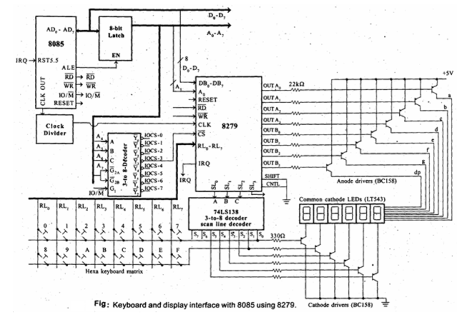
- The circuit has 6 numbers of 7-segment LEDs and so the 8279 has to be programmed in encoded scan. (Because in decoded scan, only 4 numbers of 7-segment LEDs can be interfaced)
- In encoded scan the output of scan lines will be binary count. Therefore, an external 3-to-8 decoder is used to decode the scan lines SL0, SL1 and SL2 of 8279 to produce eight scan lines S0 to S7.
- The decoded scan lines S0 and S1 are common for keyboard and display.
- The decoded scan lines S2 to S5 are used only for display and the decoded scan lines S6 and S7 are not used in the system.
- Anode and Cathode drivers are provided to take care of the current requirement of LEDs.
- The pnp transistors, BC 158 are used as driver transistors.
- The anode drivers are called segment drivers and cathode drivers are called digit drivers.
- The 8279 output the display code for one digit through its output lines (OUT A0 to OUT A3 and OUT B0 to OUT B3) and send a scan code through, SL0- SL3.
- The display code is inverted by segment drivers and sent to segment bus.
- The scan code is decoded by the decoder and turns ON the corresponding digit driver. Now one digit of the display character is displayed. After a small interval (10 milli-second, typical), the display is turned OFF (i.e., display is blanked) and the above process is repeated for next digit. Thus multiplexed display is performed by 8279.
- The keyboard matrix is- formed using the return lines, RL0 to RL3 of 8279 as columns and decoded scan lines S0 and S1 as rows.
- A hexa key is placed at the crossing point of each row and column. Any key pressed will short that particular row and column. Normally the column and row line will be high.
- While scanning 8279 will output binary count on SL0 to SL3, which is decoded by decoder to make a row as zero. When a row is zero the 8279 reads the columns. If a key is pressed, then the corresponding column will be zero.
- If 8279 detects a key pressed then it wait for debounce time and again read the columns to generate key code.
- In encoded scan keyboard mode, the 8279 stores an 8-bit code for each valid key press. The keycode consist of the binary value of the column and row in which the key is found and the status of shift and control key.
- After the scan time, the next row is made zero and the process is repeated . Thus 8279 continuously scan the keyboard.
INTEL 8279 is specially developed for interfacing keyboard and display devices to 8085/8086/8088 microprocessor- based system.
Some of the features include:
- Simultaneous keyboard and display operations.
- Scanned keyboard mode.
- Scanned sensor mode.
- 8-character keyboard FIFO.
- 1 6-character display.
- Right or left entry 1 6-byte display RAM.
- Programmable scan timing.
The four major sections of 8279 are keyboard, scan, display and CPU interface.
Keyboard section:
- The keyboard section consists of eight return lines RL0 - RL7 that can be used to form the columns of a keyboard matrix.
- Shift and control/strobe are additional inputs. The keys are automatically debounced.
- The two operating modes of keyboard section are 2-key lockout and N-key rollover.
- In the 2-key lockout mode, if two keys are pressed simultaneously, the first key is recognized.
- In the N-key rollover mode simultaneous keys are recognized and their codes are stored in FIFO.
- The keyboard section consists of 8 x 8 FIFO RAM.
- The FIFO can store eight key codes in the scan keyboard mode. The status of the shift key and control key are also stored along with key code.
- The 8279 generate an interrupt signal when there is an entry in FIFO. The format of key code entry in FIFO for scan keyboard mode is,
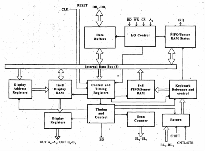
- The functional block diagram of 8279 is shown.

- In sensor matrix mode the open/close status condition of 64 switches is stored in FIFO RAM. If the condition of any of the switches changes then the 8279 asserts IRQ as high to interrupt the processor.
Display section:
- The display section has eight output lines divided into two groups A0-A3 and B0-B3.
- The output lines can be used either as a single group of eight lines or as two groups of four lines, in conjunction with the scan lines for a multiplexed display.
- The output lines are connected to the anodes through driver transistor in case of common cathode 7-segment LEDs.
- The cathodes are connected to scan lines through driver transistors.
- The display can be blanked by BD (low) line.
- The display section consists of 16 x 8 display RAM. The CPU can read from or write into any location of the display RAM.
Scan section:
- The scan section has a scan counter and four scan lines, SL0 to SL3.
- In decoded scan mode, the output of scan lines is similar to a 2-to-4 decoder.
- In encoded scan mode, the output of scan lines will be binary count, therefore the external decoder should be used to convert the binary count to decoded output.
- The scan lines are common for keyboard and display.
- The scan lines are used to form the rows of a matrix keyboard also connected to digit drivers of a multiplexed display, to turn ON/OFF.
CPU interface section:
- The CPU interface section takes care of data transfer between 8279 and the processor.
- It has eight bidirectional data lines DB0 to DB7 for data transfer between 8279 and CPU.
- It requires two internal address A =0 for selecting data buffer and A = 1 for selecting control register of 8279.
- The control signals WR (low), RD (low), CS (low) and A0 are used for read/write to 8279.
- It has an interrupt request line IRQ, for interrupt driven data transfer with processor.
- The 8279 require an internal clock frequency of 100 kHz. This can be obtained by dividing the input clock by an internal pre-scaler.
- The RESET signal sets the 8279 in 16-character display with two -key lockout keyboard modes.
8254 is a device designed to solve the timing control problems in a microprocessor. It has 3 independent counters, each capable of handling clock inputs up to 10 MHz and size of each counter is 16 bit. It operates in +5V regulated power supply and has 24 pin signals. All modes are software programmable. The 8254 is an advanced version of 8253 which did not offered the feature of read back command.
The basic block diagram of 8254 is:
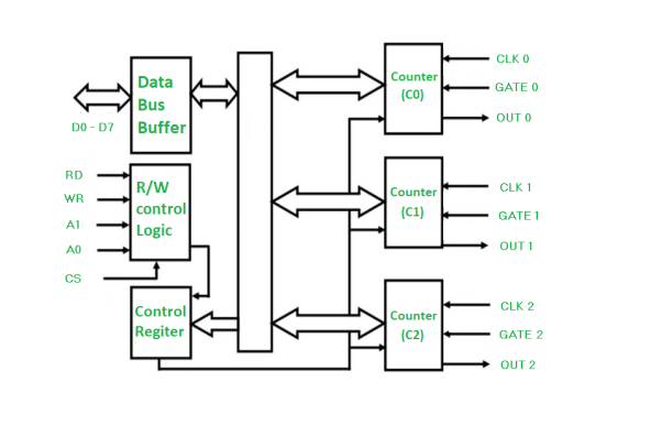
It has 3 counters each with two inputs (Clock and Gate) and one output. Gate is used to enable or disable counting. When any value of count is loaded and value of gate is set(1), after every step value of count is decremented by 1 until it becomes zero.
Depending upon the value of CS, A1 and A0 we can determine addresses of selected counter.
CS | A1 | A0 | SELECETION |
0 | 0 | 0 | C0 |
0 | 0 | 1 | C1 |
0 | 1 | 0 | C2 |
0 | 1 | 1 | Control Register |
Applications –
- To generate accurate time delay
- As an event counter
- Square wave generator
- Rate generator
- Digital one shot
8251 universal synchronous asynchronous receiver transmitter (USART) acts as a mediator between microprocessor and peripheral to transmit serial data into parallel form and vice versa.
- It takes data serially from peripheral (outside devices) and converts into parallel data.
- After converting the data into parallel form, it transmits it to the CPU.
- Similarly, it receives parallel data from microprocessor and converts it into serial form.
- After converting data into serial form, it transmits it to outside device (peripheral).
Block Diagram of 8251 USART –
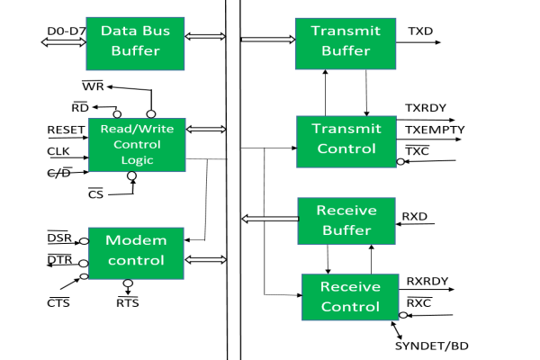
It contains the following blocks:
- Data bus buffer –
This block helps in interfacing the internal data bus of 8251 to the system data bus. The data transmission is possible between 8251 and CPU by the data bus buffer block.
2. Read/Write control logic –
It is a control block for overall device. It controls the overall working by selecting the operation to be done. The operation selection depends upon input signals as:
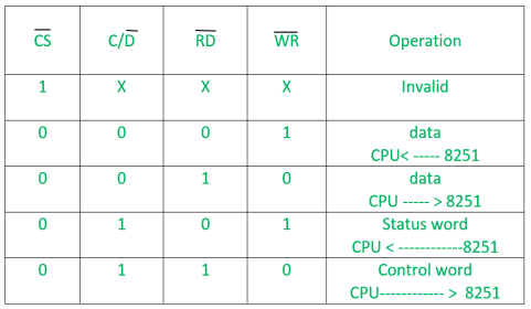
In this way, this unit selects one of the three registers- data buffer register, control register, status register.
3. Modem control (modulator/demodulator) –
A device converts analog signals to digital signals and vice-versa and helps the computers to communicate over telephone lines or cable wires. The following are active-low pins of Modem.
- DSR: Data Set Ready signal is an input signal.
- DTR: Data terminal Ready is an output signal.
- CTS: It is an input signal which controls the data transmit circuit.
RTS: It is an output signal which is used to set the status RTS.
- Transmit buffer –
This block is used for parallel to serial converter that receives a parallel byte for conversion into serial signal and further transmission onto the common channel.- TXD: It is an output signal, if its value is one, means transmitter will transmit the data.
- Transmit control –
This block is used to control the data transmission with the help of following pins:- TXRDY: It means transmitter is ready to transmit data character.
- TXEMPTY: An output signal which indicates that TXEMPTY pin has transmitted all the data characters and transmitter is empty now.
- TXC: An active-low input pin which controls the data transmission rate of transmitted data.
- Receive buffer –
This block acts as a buffer for the received data.- RXD: An input signal which receives the data.
- Receive control –
This block controls the receiving data.- RXRDY: An input signal indicates that it is ready to receive the data.
- RXC: An active-low input signal which controls the data transmission rate of received data.
- SYNDET/BD: An input or output terminal. External synchronous mode-input terminal and asynchronous mode-output terminal.
The PIC microcontroller is based on RISC architecture. Its memory architecture follows the Harvard pattern of separate memories for program and data, with separate buses.
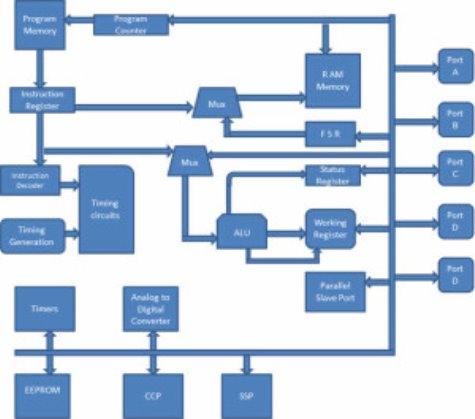
PIC microcontroller architecture
1. Memory Structure
The PIC architecture consists of two memories: Program memory and Data memory.
Program Memory: This is a 4K*14 memory space. It is used to store 13-bit instructions or the program code. The program memory data is accessed by the program counter register that holds the address of the program memory. The address 0000H is used as reset memory space and 0004H is used as interrupt memory space.
Data Memory: The data memory consists of the 368 bytes of RAM and 256 bytes of EEPROM. The 368 bytes of RAM consists of multiple banks. Each bank consists of general-purpose registers and special function registers.
The special function registers consist of control registers to control different operations of the chip resources like Timers, ADC, Serial ports, I/O ports, etc. For example, the TRISA register whose bits can be changed to alter the input or output operations of the port A.
The general-purpose registers consist of registers that are used to store temporary data and processing results of the data. These general-purpose registers are each 8-bit registers.
Working Register: It consists of a memory space that stores the operands for each instruction. It also stores the results of each execution.
Status Register: The bits of the status register denotes the status of the ALU (arithmetic logic unit) after every execution of the instruction. It is also used to select any one of the 4 banks of the RAM.
File Selection Register: It acts as a pointer to any other general-purpose register. It consists of a register file address, and it is used in indirect addressing.
Another general-purpose register is the program counter register, which is a 13-bit register. The 5 upper bits are used as PCLATH (Program Counter Latch) to independently function as any other register, and the lower 8-bits are used as the program counter bits. The program counter acts as a pointer to the instructions stored in the program memory.
EEPROM: It consists of 256 bytes of memory space. It is a permanent memory like ROM, but its contents can be erased and changed during the operation of the microcontroller. The contents into EEPROM can be read from or written to, using special function registers like EECON1, EECON, etc.
2. I/O Ports
PIC16 series consists of five ports, such as Port A, Port B, Port C, Port D, and Port E.
Port A: It is a 16-bit port, which can be used as an input or output port based on the status of the TRISA register.
Port B: It is an 8-bit port, which can be used as both an input and output port. 4 of its bits, when used as input, can be changed upon interrupt signals.
Port C: It is an 8-bit port whose operation (input or output) is determined by the status of the TRISC register.
Port D: It is an 8-bit port, which apart from being an I/O port, acts as a slave port for connection to the microprocessor bus.
Port E: It is a 3-bit port that serves the additional function of the control signals to the A/D converter.
3. Timers
PIC microcontrollers consist of 3 timers, out of which the Timer 0 and Timer 2 are 8-bit timers and the Time-1 is a 16-bit timer, which can also be used as a counter.
4. A/D Converter
The PIC Microcontroller consists of 8-channels, 10-bit Analog to Digital Converter. The operation of the A/D converter is controlled by these special function registers: ADCON0 and ADCON1. The lower bits of the converter are stored in ADRESL (8 bits), and the upper bits are stored in the ADRESH register. It requires an analog reference voltage of 5V for its operation.
5. Oscillators
Oscillators are used for timing generation. PIC microcontrollers consist of external oscillators like crystals or RC oscillators. In the case of crystal oscillators, the crystal is connected between two oscillator pins, and the value of the capacitor connected to each pin determines the mode of operation of the oscillator. The different modes are low-power mode, crystal mode, and the high- speed mode. In the case of RC oscillators, the value of the Resistor and Capacitor determines the clock frequency. The clock frequency ranges from 30 kHz to 4 MHz.
6. CCP module:
A CCP module works in the following three modes:
Capture Mode: This mode captures the time of arrival of a signal, or in other words, captures the value of the Timer1 when the CCP pin goes high.
Compare Mode: It acts as an analog comparator that generates an output when the timer1 value reaches a certain reference value.
PWM Mode: It provides PWM output with a 10-bit resolution and programmable duty cycle.
DAC:
The three steps of interfacing of 8255 with 8085 that are :
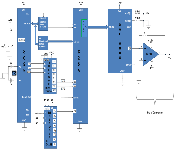
The DAC 0808 is 8-bit digital to analog convertor IC. It converts digital data into equivalent analog current.
Therefore I to V converter is used to convert analog output current of DAC to equivalent analog voltage.
PA0-PA7 pins of Port A are connected to D0-D7 pins of DAC.
In above DAC dual power supply of +/- 10V is applied with reference voltage 10V as shown in diagram.
According to theory of DAC Equivalent analog output is given as:
V0=Vref
Ex:
1. If data =00H [00000000], Vref= 10V
V0= 0 Volts.
2. If data is 80H [10000000], Vref= 10V V0=10
V0= 5 Volts.
The control word format of 8255 for above interfacing is given as: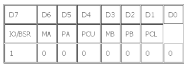 =80H
=80H
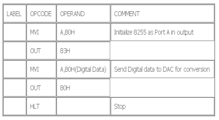
Program:
Interfacing Diagram of DAC
ADC :
ADC Interfacing with 8085 Microprocessor
1 Features
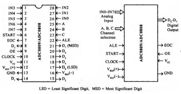 Pin Diagram of ADC 0808
ü The ADC0809 is an 8-bit successive approximation type ADC with inbuilt 8-channel multiplexer.
ü The ADC0809 is suitable for interface with 8086 microprocessor.
ü The ADC0809 is available as a 28 pin IC in DIP (Dual Inline Package).
ü The ADC0809 has a total unadjusted error of ±1 LSD (Least Significant Digit).
ü The ADC0808 is also same as ADC0809 except the error. The total unadjusted error in ADC0808 is ± 1/2 LSD.
Block Diagram of ADC 0809
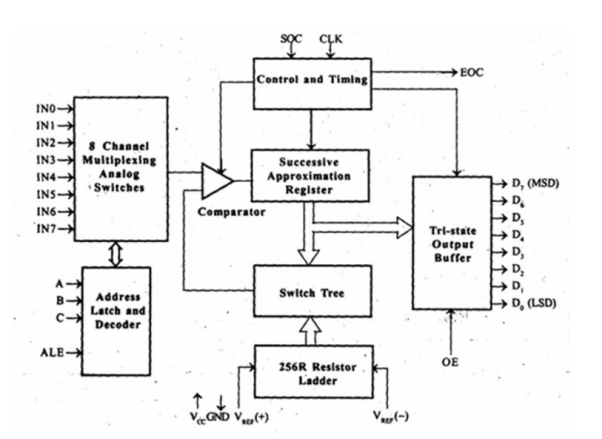
The successive approximation register (SAR) performs eight iterations to determine the digital code for input value.
The SAR is reset on the positive edge of START pulse and start the conversion process on the falling edge of START pulse. A conversion process will be interrupted on receipt of new START pulse.
The End-Of-Conversion (EOC) will go low between 0 and 8 clock pulses after the positive edge of START pulse.
The ADC can be used in continuous conversion mode by tying the EOC output to START input. In this mode an external START pulse should be applied whenever power is switched ON.
The 256R ladder network has been provided instead of conventional R/2R ladder because of its inherent monotonic, which guarantees no missing digital codes.
Also the 256R resistor network does not cause load variations on the reference voltage.
The comparator in ADC0809/ADC0808 is a chopper- stabilized comparator. It converts the DC input signal into an AC signal, and amplifies the AC sign using high gain AC amplifier.
Then it converts AC signal to DC signal. This technique limits the drift component of the amplifier because the drift is a DC component and it is not amplified/passed by the AC amp1ifier.
This makes the ADC extremely insensitive to temperature, long term drift and input offset errors. In ADC conversion process the input analog value is quantized and each quantized analog value will have a unique binary equivalent. The quantization step in ADC0809/ADC0808 is given by,
Q step = Vref/ 2 8 = Vref(+) – Vref(-)/ 25610
The digital data corresponding to analog input is
Digital data = (Vin/Qstep – 1) 10
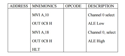
PROGRAM
LCD:
INTERFACING LCD
Features:
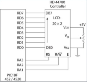
• Hardware • 20 x 2-line LCD display
• Two lines with 20 characters per line
• LCD has a display Data RAM
• Stores data in 8-bit character code
• Each register in Data RAM has its own address
• Corresponds to its position on the line
• Line 1 is 00H to 13H
• Line 2 is 40H to 53H 3
•Driver HD44780
•8-bit data bus (RD7-RD0)
•Three control signals
• RS – Register Select (RA3)
• R/W – Read/Write (RA2)
• E – Enable (RA1)
•Three power connections • Power, ground, and variable resistor to control brightness
INTERFACING LCD
•Can be interfaced either in 8-bit mode or 4-bit mode
•In 8-bit mode, all eight data lines are connected
•In 4-bit mode, only four data lines are connected
• Two transfers per character (or instruction) are needed
•Driver has two 8-bit internal registers
•Instruction Register (IR) to write instructions to set up LCD
LCD Operation •When the MPU writes an instruction to IR or data to DR, the controller: •Sets DB7 high indicating that the controller is busy •Sets DB7 low after the completion of the operation •The MPU should always check whether DB7 is low before sending an instruction 7
INTERFACING LCD
•Writing to or Reading from LCD
•The MPU:
•Asserts RS low to select IR
•Asserts RS high to select DR
•Reads from LCD by asserting the R/W signal high
•Writes into LCD by asserting the R/W signal low 8
To write into the LCD
• Send the initial instructions to set up the LCD
• 4-bit or 8-bit mode
• Continue to check DB7 until it goes low
• Write instructions to IR to set up LCD parameters
• Number of display lines and cursor status
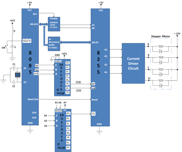
Stepper Motor :
Stepper motor is an electromechanical device that rotates through fixed angular steps when digital inputs are applied. It is suitable for precise position, speed and direction control which are required in automation system.
The angle through which stepper motor rotates with a fixed angle for each digital data is called step angle.
Different stepper motor has different step angle. The more frequently used stepper motor has step angle of 0.9 degrees and 1.8 degrees.
Depending on the sequence applied to stepper motor, it can be classified in two category:
1. 4- Step sequence or full step sequence
2. 8- Step sequence or half step sequence
Calculations:
1. Total no. Of steps=
Ex: = 200 steps are required to complete one rotation
2. Total no. Of repeated steps=
Ex: = 50 repetition of sequence = (32) in Hexadecimal.
4-Step sequence:
In this type of functioning, the following 4 binary sequence/code are used for rotation: (Considering step angle= 1.8 degrees)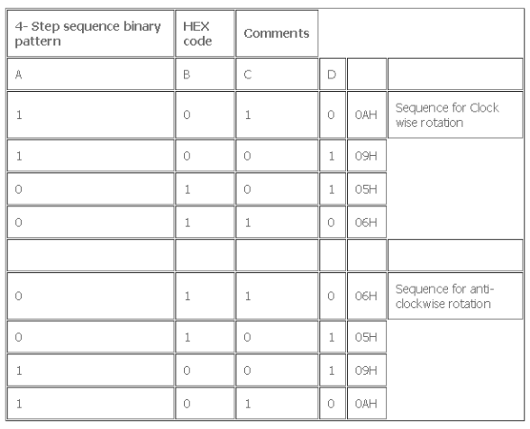
8-Step Sequence:
In this type of functioning, the following 8 binary sequence/code are used for rotation: (Considering step angle= 0.9degrees)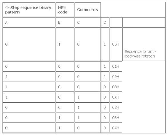
Chips select Logic: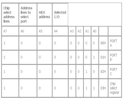
Control word Format: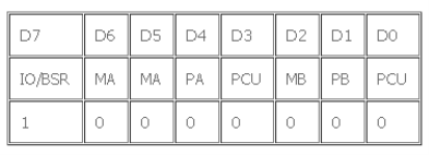 =80H
=80H
Program: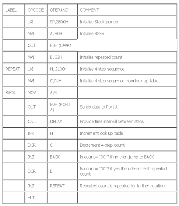
In the above program in look up table if the 4-step sequence for clock wise then stepper motor will rotate in clockwise direction and if the 4-step sequence for anti-clock wise then stepper motor will rotate in anti-clockwise direction.
Speed control of stepper motor is achieved by writing program to rotate stepper motor continuously in delay program. We can change the delay between two steps and thus change the speed of stepper motor.
Interfacing diagram of Stepper motor with 8085
References:
Microprocessor Architecture, Programming, and Applications with the 8085 Textbook by Ramesh S. Gaonkar
Microprocessor 8085 and Its Interfacing Book by Mathur Sunil
8085 MICROPROCESSOR: PROGRAMMING AND INTERFACING
Book by N. K. SRINATH