Unit 1
IC Fabrication
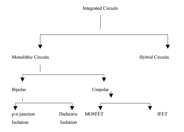
Integrated circuit (IC)
ICs have made significance in the technology development of the 21st century. It has changed the world of electronics as well as reduced the size of electronics from refrigerator size to a palm size.
Initially vacuum tubes were used but IC’s dissipates less heat and consumes less energy when compared to vacuum tubes. Also, IC’s are reliable than vacuum tubes.
ICs have changed the design from discrete electronic components to hybrid solid state devices which combine discrete components with ICs.
At present ICs are so small that connections can be seen only through microscope. Thus, ICs are immensely used in electronics and control all devices.
IC consists of transistors, capacitors, resistors, diodes etc. These are interconnected with external connection terminals in small package.
ICs are classified into:
Below is the classification of different types of ICs basis on their chip size.
SSI : Small scale integration. 3 – 30 gates per chip.
MSI : Medium scale integration. 30 – 300 gates per chip.
LSI : Large scale integration. 300 – 3,000 gates per chip.
VLSI : Very large- scale integration. More than 3,000 gates per chip.
The first integrated circuits contained only a few transistors. Called "Small-Scale Integration" (SSI), digital circuits containing transistors numbering in the tens provided a few logic gates
The term Large Scale Integration was first used by IBM scientist Rolf Landauer when describing the theoretical concept, from there came the terms for SSI, MSI, VLSI, and ULSI.
They began to appear in consumer products at the turn of the decade, a typical application being FM inter-carrier sound processing in television receivers.
The next step in the development of integrated circuits, taken in the late 1960s, introduced devices which contained hundreds of transistors on each chip, called "Medium-Scale Integration" (MSI). They were attractive economically because while they cost little more to produce than SSI devices, they allowed more complex systems to be produced using smaller circuit boards, less assembly work (because of fewer separate components), and a number of other advantages.
VLSI The final step in the development process, starting in the 1980s and continuing through the present, was "very large-scale integration" (VLSI). The development started with hundreds of thousands of transistors in the early 1980s, and continues beyond several billion transistors as of 2007.
In 1986 the first one- megabit RAM chips were introduced, which contained more than one million transistors. Microprocessor chips passed the million transistor mark in 1989 and the billion transistor mark in 2005
ULSI, WSI, SOC and 3D-IC: To reflect further growth of the complexity, the term ULSI that stands for "Ultra-Large- Scale Integration" was proposed for chips of complexity of more than 1 million transistors.
Wafer-scale integration (WSI) is a system of building very-large integrated circuits that uses an entire silicon wafer to produce a single "super-chip". Through a combination of large size and reduced packaging, WSI could lead to dramatically reduced costs for some systems, notably 8 massively parallel supercomputers.
The name is taken from the term Very-Large-Scale Integration, the current state of the art when WSI was being developed.
System-on-a-Chip (SoC or SOC) is an integrated circuit in which all the components needed for a computer or other system is included on a single chip. The design of such a device can be complex and costly, and building disparate components on a single piece of silicon may compromise the efficiency of some elements.
Three- Dimensional Integrated Circuit (3D-IC) has two or more layers of active electronic components that are integrated both vertically and horizontally into a single circuit.
A sample circuit must is considered to be converted to its monolithic form with the basic components like resistor, diode, and transistor forms a basic circuit.
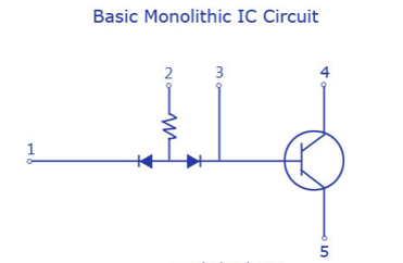
After the basic circuit, the different layers for the monolithic IC are then considered.
The basic structure of a monolithic IC has 4 layers of different materials.
The base layer will be a P-type silicon layer named as the substrate layer. This layer will have a typical thickness of 200 micrometer.
The layer above the substrate P-type silicon layer is the N-type layer. All the active and passive components required for the circuit are fabricated onto this layer. This layer has a typical thickness of 25 micrometer. T
The N-type silicon material is grown as a single crystal extension of the P-layer and the components are required are fabricated using series of P-type and N-type impurity diffusions.
The N-type layer becomes the collector for the transistor or an element for a diode or a capacitor.
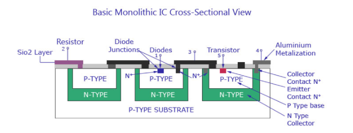
The layer above N-type is made of silicon dioxide (SiO2) material. Since there is a selective P-type and N-type impurity diffusion going on in the second layer, this layer acts as a barrier in the process.
This layer is etched away from the region where diffusion is desired to be permitted with photolithographic process. The rest of the wafer remains protected against diffusion. This layer also protects the silicon layer from contamination.
The up-most layer is that made of aluminium. This metallic layer is used to provide interconnections between the different components used in IC.
The first step in transistor fabrication is creation of the collector region. We require a low resistivity path for the collector current. This is because the collector contact is normally taken at the top, thus increasing the collector series resistance and the VCE(Sat) of the device.
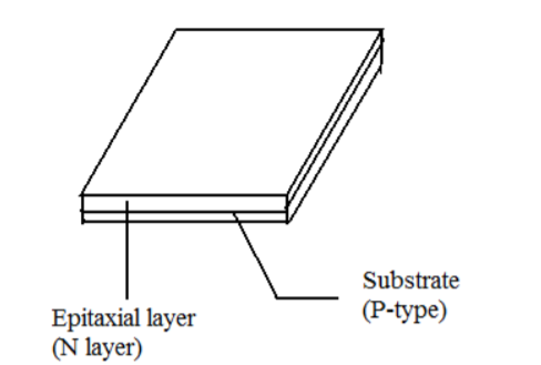
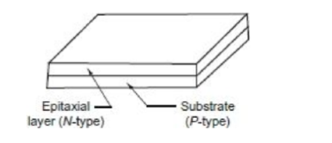
The higher collector resistance is reduced by a process called buried layer as shown in figure.
In this arrangement, a heavily doped ‗N‘ region is sandwiched between the N-type epitaxial layer and P – type substrate. This buried N+ layer provides a low resistance path in the active collector 10 region to the collector contact C.
In effect, the buried layer provides a low resistance shunt path for the flow of current.
For fabricating an NPN transistor a P-type silicon substrate having a resistivity of typically 1Ω-cm, corresponding to an acceptor ion concentration of 1.4 * 10 15 atoms/cm3 . An oxide mask with the necessary pattern for buried layer diffusion is prepared. This is followed by masking and etching the oxide in the buried layer mask.
The junction depth is typically a few microns, with sheet resistivity of around 20Ω per square. Then, an epitaxial layer of lightly doped N-silicon is grown on the P-type substrate by placing the wafer in the furnace at 1200 0 C and introducing a gas containing phosphorus (donor impurity).
The resulting structure is shown in figure. The subsequent diffusions are done in this epitaxial layer. All active and passive components are formed on the thin N-layer epitaxial layer grown over the P-type substrate. Obtaining an epitaxial layer of the proper thickness and doping with high crystal quality is perhaps the most formidable challenge in bipolar device processing.
Masking is used to protect some area of wafer when working on another area. For this
Photolithographic process is used
Photographic mask is used
Application of photoresistive film on the wafer
The alignment of wafer to mask using photo aligner
Exposing wafer to UV light through mask using automatic tools for alignment purpose.
Etching is the process of using strong acid or etchant to cut into the unprotected parts of a metal surface to create a design.
• Etching is used in microfabrication to chemically remove layers from the surface of a wafer during manufacturing.
• Etching is a critically important process module, and every wafer undergoes many etching steps before it is complete.
• For many etch steps, part of the wafer is protected from the etchant by a "masking" material which resists etching. The masking material is a photoresist which has been patterned using photolithography.
Two main methods of etching: • wet etching • dry etching
Diffusion is a process by which atoms move from a high-concentration region to a low concentration region. This is very much like a drop of ink dispersing through a glass of water except that it occurs much more slowly in solids. In VLSI fabrication, this is a method to introduce impurity atoms (dopants) into silicon to change its resistivity. The rate at which dopants diffuse in silicon is a strong function of temperature. Diffusion of impurities is usually carried out at high temperatures (1000–1200°C) to obtain the desired doping profile. When the wafer is cooled to room temperature, the impurities are essentially “frozen” in position.

The diffusion process is performed in furnaces similar to those used for oxidation. The depth to which the impurities diffuse depends on both the temperature and the processing time. The most common impurities used as dopants are boron, phosphorus, and arsenic. Boron is a p-type dopant, while phosphorus and arsenic are n-type dopants. These dopants can be effectively masked by thin silicon dioxide layers. By diffusing boron into an n-type substrate, a p-n junction is formed (diode). If the doping concentration is heavy, the diffused layer can also be used as a conducting layer with less resistivity.
The monolithic fabrication process consists of wafer preparation, epitaxial growth, diffused isolation, base and emitter diffusions, pre-ohmic etch, metallization, dicing, mounting and packaging, wire bonding, encapsulation and final testing.
Wafer Preparation:
The wafer is a round slice of semiconductor material such as silicon. Silicon is preferred due to its characteristics which forms the base or substrate for entire chip.
First purify polycrystalline silicon created from the sand. Then heat to produce molten liquid. A small piece of solid silicon is dipped in the molten liquid. Then the solid silicon (seed) is gently pulled from the melt. The liquid cools to form single crystal ingot.
When wafer is sliced, the surface will be damaged. It can be smoothening by polishing. After polishing the wafer, it is thoroughly clean and dried. The wafers are cleaned by using high purity low particle chemicals. The silicon wafers are exposed to ultra-pure oxygen.
Epitaxial growth
It means the growing of single silicon crystal upon original silicon substrate. A uniform layer of silicon dioxide is formed on the surface of wafer.
Isolation diffusion
The IC contains many devices and since numbers of devices are to be fabricated on the same IC chip it becomes necessary to provide good isolation between various components and their interconnections.
The most important techniques for isolation are:
- PN junction isolation
- Dielectric isolation
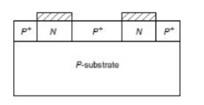
In PN junction isolation technique the P+ type impurities are selectively into the N-type epitaxial layer so that it touches P-type substrate at bottom.
If the P substrate is held at negative potential the diode will be reverse biased providing isolation between the islands. The individual components are fabricated inside these islands. This method is economical and used for general purpose integrated circuits.
In PN junction isolation technique the P+ type impurities are difused into N-type epitaxial layer so that the P-type substrate at the bottom. This methods generates N-type isolation regions surrounded by P-type moats.
In dielectric isolation method a layer of solid dielectric such as silicon dioxide or ruby surrounds each componentand this dielectric provides isolation.
Base and Emitter Diffusion
Base Diffusion:
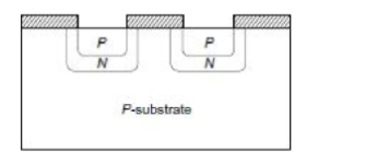
This diffusion is done in two steps pre-deposition of dopants at 900 0 C driving them in at about 1200 0 C. The drive-in is done in an oxidising ambience so that oxide is grown over the base region for subsequent steps.
The figure shows how P-type base region of the transistor diffused in the N-type island using photolithography and isolation diffusion process.
Emitter Diffusion
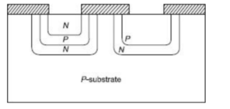
The emitter diffusion process is the final step in the fabrication of the transistor. The emitter opening must lie wholly within the base. Emitter masking not only opens windows for the emitter but also the contact point which provides low resistivity ohmic contact path for the emitter material.
Pre-Ohmic Etch
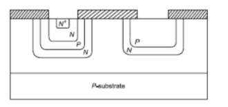
After the fabrication of emitter windows are etched into N-type regions where contacts are made for collector and emitter terminals. Heavily concentrated phosphorus N+ dopant is diffused into these regions simultaneously.
Metallization
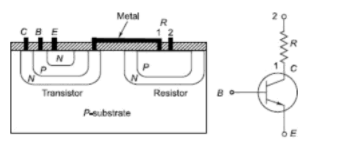
Metallisation NPN transistor
The IC chip is now complete with the active and passive devices and the metal leads are formed for making connections with the terminals of the device.
Aluminium is deposited over the entire wafer by vacuum deposition. The thickness for single layer is a fraction of m. Metallisation is carried out by evaporating aluminium over the entire surface and then selectively etching away aluminium to leave behind the desired interconnection and bonding pads as shown.
Wafer dicing
This is the process by which dies are separated from a wafer of semiconductor. During dicing, wafers are typically mounted on dicing tape (foil). The adhesive tape on which the wafer is mounted ensures that the individual dies remain firmly in place during dicing. Once a wafer has been diced, the pieces left on the dicing tape are referred to as die, dice or dies.
Wire bonding
There are basically two forms of wire bonds, Wedge bonds and Ball bonds. Recent industry survey shows that about 90% of all electronic packages and assemblies are produced using ball bonds and about 10% are produced with wedge bonds.
Encapsulation
In the encapsulation stage, the die is encapsulated with ceramic, plastic, or epoxy to prevent physical damage or corrosion. As in other packaging stages, the customer has to take into account encapsulation requirement such as hermetic sealing, moisture contamination, physical package options, sensitivity of the dies to stress from packaging materials, height requirement of the capped devices, multi-die capability, etc.
Final testing
The IC packaging is then sealed either by sintering and binding powders to seal off the ceramic package or use moulded plastic caps to seal off the plastic package.
With the packaging completed, each IC chip must pass through one final test to determine if any further chips were damaged during packaging and to gauge the performance of each device.
The ICs are tested depending on their expected use therefore a chip which is to be used at high temperature environment, would have testing on the lines of probing a sample after it is exposed to elevated temperatures for a period of time. The IC chips are then sealed in anti-static plastic bags and are sent to be stored or shipped to the buyer.
Diodes
Diodes are fabricated by the same diffusion process as transistors the only difference is that only two of the regions are used to form one P-N junction.
In figure, collector-base junction of the transistor is used as a diode. Anode of the diode is formed during the base diffusion of the transistor and the collector region of the transistor becomes the cathode of the diode.
For high speed switching emitter base junction is used as a diode.
Resistors
The resistors used in IC’s are given respective ohmic value by varying the concentration of doping impurity and depth of diffusion.
The range of resistor values that may be produced by the diffusion process varies from ohms to hundreds of kilohms.
On the other hand, if all the resistors are diffused at the same time, then the tolerance ratio may be good.
Most resistors are formed during the base diffusion of the integrated transistor, as shown in figure below. This is because it is the highest resistivity region.
For low resistance values, emitter region is used as it has much lower resistivity.
Another diffusion technique is also used for the growth of IC resistors. It is basically a thin-film technique.
In this process a metal film is deposited on a glass or Si02 surface. The resistance value can be controlled by varying thickness, width, and length of the film.
Since diffused resistors can be processed while diffusing transistors. This technique is more economic and less time consuming and therefore widely used.
Capacitors
The figure below shows the P and N-regions forming the capacitor plates. The dielectric of the capacitor is the depletion region between them.
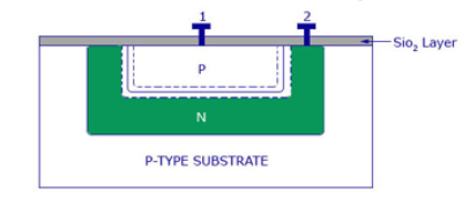
All P-N junctions have capacitance such that the capacitors may be produced by fabricating junctions. The amount of change in the reverse bias varies the value of junction capacitance as well as the depletion width. The value may be as less as 100 picoFarads.
Using the silicon dioxide as a dielectric may also be a way to fabricate capacitors. One plate of the capacitors is formed by diffusing a heavily doped N-region. The other plate of the capacitor is formed by depositing a film of aluminium on the silicon dioxide dielectric on the wafer surface.
For such a capacitor, a voltage of any polarity can be used, and when comparing a diffused capacitor with such a capacitor the diffused capacitor may have small values of breakdown voltage.
FETs
A field effect transistor (FET) using an organic semiconductor in its channel is basically called an organic FET. A thin film transistor (TFT) is one of the classifications of OFET’s. The thin film technology plays an important role in developing energy efficient devices and storage.
In the fabrication process, top contact and bottom gate structure of OTFT was used.
For the deposition of various organic layers (dielectric layer and the semiconductor layer) spin coating and vapor evaporation techniques have been utilized.
Glass is used as a substrate in this structure with perovskite material as the active layer.
After the complete fabrication of the device, it is being tested for its characteristic’s curves, for validating the efficiency of the device.
References:
IC fabrication technology by Gouranga bose.
Integrated Circuit fabrication technology by David J Elliot
Understanding Fabless IC Technology (English, Electronic book text, HurtarteJeorge S)