UNIT - 2
Memory system
A memory unit is an essential component in any digital computer since it is needed for storing programs and data.
Typically, a memory unit can be classified into two categories:
The memory unit that establishes direct communication with the CPU is called Main Memory. The main memory is often referred to as RAM (Random Access Memory).
The memory units that provide backup storage are called Auxiliary Memory. For instance, magnetic disks and magnetic tapes are the most commonly used auxiliary memories.
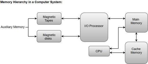
Apart from the basic classifications of a memory unit, the memory hierarchy consists all of the storage devices available in a computer system ranging from the slow but high-capacity auxiliary memory to relatively faster main memory.
The following image illustrates the components in a typical memory hierarchy.
|
Figure 1 – Memory hierarchy in a computer system
Auxiliary Memory
Auxiliary memory is known as the lowest-cost, highest-capacity and slowest-access storage in a computer system. Auxiliary memory provides storage for programs and data that are kept for long-term storage or when not in immediate use. The most common examples of auxiliary memories are magnetic tapes and magnetic disks.
A magnetic disk is a digital computer memory that uses a magnetization process to write, rewrite and access data. For example, hard drives, zip disks, and floppy disks.
Magnetic tape is a storage medium that allows for data archiving, collection, and backup for different kinds of data.
Main Memory
The main memory in a computer system is often referred to as Random Access Memory (RAM). This memory unit communicates directly with the CPU and with auxiliary memory devices through an I/O processor.
The programs that are not currently required in the main memory are transferred into auxiliary memory to provide space for currently used programs and data.
I/O Processor
The primary function of an I/O Processor is to manage the data transfers between auxiliary memories and the main memory.
Cache Memory
The data or contents of the main memory that are used frequently by CPU are stored in the cache memory so that the processor can easily access that data in a shorter time. Whenever the CPU requires accessing memory, it first checks the required data into the cache memory. If the data is found in the cache memory, it is read from the fast memory. Otherwise, the CPU moves onto the main memory for the required data.
Main Memory
The main memory acts as the central storage unit in a computer system. It is a relatively large and fast memory which is used to store programs and data during the run time operations.
The primary technology used for the main memory is based on semiconductor integrated circuits. The integrated circuits for the main memory are classified into two major units.
RAM (Random Access Memory) integrated circuit chips
ROM (Read Only Memory) integrated circuit chips
RAM integrated circuit chips
The RAM integrated circuit chips are further classified into two possible operating modes, static and dynamic.
The primary compositions of a static RAM are flip-flops that store the binary information. The nature of the stored information is volatile, i.e. it remains valid as long as power is applied to the system. The static RAM is easy to use and takes less time performing read and write operations as compared to dynamic RAM.
The dynamic RAM exhibits the binary information in the form of electric charges that are applied to capacitors. The capacitors are integrated inside the chip by MOS transistors. The dynamic RAM consumes less power and provides large storage capacity in a single memory chip.
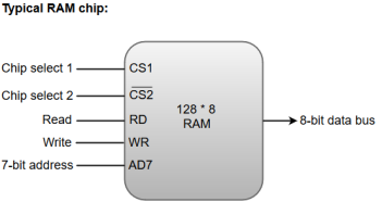
RAM chips are available in a variety of sizes and are used as per the system requirement. The following block diagram demonstrates the chip interconnection in a 128 * 8 RAM chip.
|
Figure 2 – Typical RAM chip
A 128 * 8 RAM chip has a memory capacity of 128 words of eight bits (one byte) per word. This requires a 7-bit address and an 8-bit bidirectional data bus.
The 8-bit bidirectional data bus allows the transfer of data either from memory to CPU during a read operation or from CPU to memory during a write operation.
The read and write inputs specify the memory operation, and the two chip select (CS) control inputs are for enabling the chip only when the microprocessor selects it.
The bidirectional data bus is constructed using three-state buffers.
The output generated by three-state buffers can be placed in one of the three possible states which include a signal equivalent to logic 1, a signal equal to logic 0, or a high-impedance state.
Note: The logic 1 and 0 are standard digital signals whereas the high-impedance state behaves like an open circuit, which means that the output does not carry a signal and has no logic significance.
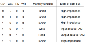
The following function table specifies the operations of a 128 * 8 RAM chip.
|
From the functional table, we can conclude that the unit is in operation only when CS1 = 1 and CS2 = 0. The bar on top of the second select variable indicates that this input is enabled when it is equal to 0.
ROM integrated circuit
The primary component of the main memory is RAM integrated circuit chips, but a portion of memory may be constructed with ROM chips.
A ROM memory is used for keeping programs and data that are permanently resident in the computer.
Apart from the permanent storage of data, the ROM portion of main memory is needed for storing an initial program called a bootstrap loader. The primary function of the bootstrap loader program is to start the computer software operating when power is turned on.
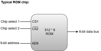
ROM chips are also available in a variety of sizes and are also used as per the system requirement. The following block diagram demonstrates the chip interconnection in a 512 * 8 ROM chip.
|
Figure 3 – Typical ROM chip
A ROM chip has a similar organization as a RAM chip. However, a ROM can only perform read operation; the data bus can only operate in an output mode.
The 9-bit address lines in the ROM chip specify any one of the 512 bytes stored in it.
The value for chip select 1 and chip select 2 must be 1 and 0 for the unit to operate. Otherwise, the data bus is said to be in a high-impedance state.
Auxiliary Memory
An Auxiliary memory is known as the lowest-cost, highest-capacity and slowest-access storage in a computer system. It is where programs and data are kept for long-term storage or when not in immediate use. The most common examples of auxiliary memories are magnetic tapes and magnetic disks.
Magnetic Disks
A magnetic disk is a type of memory constructed using a circular plate of metal or plastic coated with magnetized materials. Usually, both sides of the disks are used to carry out read/write operations. However, several disks may be stacked on one spindle with read/write head available on each surface.
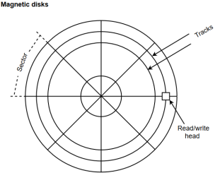
The following image shows the structural representation for a magnetic disk.
|
Figure 4 – Magnetic disks
The memory bits are stored in the magnetized surface in spots along the concentric circles called tracks.
The concentric circles (tracks) are commonly divided into sections called sectors.
Magnetic Tape
Magnetic tape is a storage medium that allows data archiving, collection, and backup for different kinds of data. The magnetic tape is constructed using a plastic strip coated with a magnetic recording medium.
The bits are recorded as magnetic spots on the tape along several tracks. Usually, seven or nine bits are recorded simultaneously to form a character together with a parity bit.
Magnetic tape units can be halted, started to move forward or in reverse, or can be rewound. However, they cannot be started or stopped fast enough between individual characters. For this reason, information is recorded in blocks referred to as records.
Associative Memory
An associative memory can be considered as a memory unit whose stored data can be identified for access by the content of the data itself rather than by an address or memory location.
Associative memory is often referred to as Content Addressable Memory (CAM).
When a write operation is performed on associative memory, no address or memory location is given to the word. The memory itself is capable of finding an empty unused location to store the word.
On the other hand, when the word is to be read from an associative memory, the content of the word, or part of the word, is specified. The words which match the specified content are located by the memory and are marked for reading.
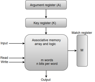
The following diagram shows the block representation of an Associative memory.
|
Figure 5 - Block representation of an Associative memory
From the block diagram, we can say that an associative memory consists of a memory array and logic for 'm' words with 'n' bits per word.
The functional registers like the argument register A and key register K each have n bits, one for each bit of a word. The match register M consists of m bits, one for each memory word.
The words which are kept in the memory are compared in parallel with the content of the argument register.
The key register (K) provides a mask for choosing a particular field or key in the argument word. If the key register contains a binary value of all 1's, then the entire argument is compared with each memory word. Otherwise, only those bits in the argument that have 1's in their corresponding position of the key register are compared. Thus, the key provides a mask for identifying a piece of information which specifies how the reference to memory is made.
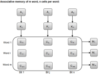
The following diagram can represent the relation between the memory array and the external registers in an associative memory.
|
Figure 6 – Associative memory of m word, n cells per word
The cells present inside the memory array are marked by the letter C with two subscripts. The first subscript gives the word number and the second specifies the bit position in the word. For instance, the cell Cij is the cell for bit j in word i.
A bit Aj in the argument register is compared with all the bits in column j of the array provided that Kj = 1. This process is done for all columns j = 1, 2, 3......, n.
If a match occurs between all the unmasked bits of the argument and the bits in word i, the corresponding bit Mi in the match register is set to 1. If one or more unmasked bits of the argument and the word do not match, Mi is cleared to 0.
Cache Memory
The data or contents of the main memory that are used frequently by CPU are stored in the cache memory so that the processor can easily access that data in a shorter time. Whenever the CPU needs to access memory, it first checks the cache memory. If the data is not found in cache memory, then the CPU moves into the main memory.
Cache memory is placed between the CPU and the main memory. The block diagram for a cache memory can be represented as:
|
The cache is the fastest component in the memory hierarchy and approaches the speed of CPU components.
The basic operation of a cache memory is as follows:
When the CPU needs to access memory, the cache is examined. If the word is found in the cache, it is read from the fast memory.
If the word addressed by the CPU is not found in the cache, the main memory is accessed to read the word.
A block of words one just accessed is then transferred from main memory to cache memory. The block size may vary from one word (the one just accessed) to about 16 words adjacent to the one just accessed.
The performance of the cache memory is frequently measured in terms of a quantity called hit ratio.
When the CPU refers to memory and finds the word in cache, it is said to produce a hit.
If the word is not found in the cache, it is in main memory and it counts as a miss.
The ratio of the number of hits divided by the total CPU references to memory (hits plus misses) is the hit ratio.
Virtual memory
A computer can address more memory than the amount physically installed on the system. This extra memory is actually called virtual memory and it is a section of a hard disk that's set up to emulate the computer's RAM.
The main visible advantage of this scheme is that programs can be larger than physical memory. Virtual memory serves two purposes. First, it allows us to extend the use of physical memory by using disk. Second, it allows us to have memory protection, because each virtual address is translated to a physical address.
Following are the situations, when entire program is not required to be loaded fully in main memory.
User written error handling routines are used only when an error occurred in the data or computation.
Certain options and features of a program may be used rarely.
Many tables are assigned a fixed amount of address space even though only a small amount of the table is actually used.
The ability to execute a program that is only partially in memory would counter many benefits.
Less number of I/O would be needed to load or swap each user program into memory.
A program would no longer be constrained by the amount of physical memory that is available.
Each user program could take less physical memory, more programs could be run the same time, with a corresponding increase in CPU utilization and throughput.
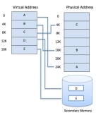
Modern microprocessors intended for general-purpose use, a memory management unit, or MMU, is built into the hardware. The MMU's job is to translate virtual addresses into physical addresses. A basic example is given below −
|
Figure 7 - Virtual addresses into physical addresses
Virtual memory is commonly implemented by demand paging. It can also be implemented in a segmentation system. Demand segmentation can also be used to provide virtual memory.
Demand Paging
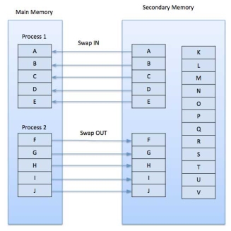
A demand paging system is quite similar to a paging system with swapping where processes reside in secondary memory and pages are loaded only on demand, not in advance. When a context switch occurs, the operating system does not copy any of the old program’s pages out to the disk or any of the new program’s pages into the main memory Instead, it just begins executing the new program after loading the first page and fetches that program’s pages as they are referenced.
|
Figure 8 - Swapping
While executing a program, if the program references a page which is not available in the main memory because it was swapped out a little ago, the processor treats this invalid memory reference as a page fault and transfers control from the program to the operating system to demand the page back into the memory.
Advantages
Following are the advantages of Demand Paging −
Large virtual memory.
More efficient use of memory.
There is no limit on degree of multiprogramming.
Disadvantages
Number of tables and the amount of processor overhead for handling page interrupts are greater than in the case of the simple paged management techniques.
Page Replacement Algorithm
Page replacement algorithms are the techniques using which an Operating System decides which memory pages to swap out, write to disk when a page of memory needs to be allocated. Paging happens whenever a page fault occurs and a free page cannot be used for allocation purpose accounting to reason that pages are not available or the number of free pages is lower than required pages.
When the page that was selected for replacement and was paged out, is referenced again, it has to read in from disk, and this requires for I/O completion. This process determines the quality of the page replacement algorithm: the lesser the time waiting for page-ins, the better is the algorithm.
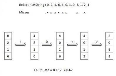
A page replacement algorithm looks at the limited information about accessing the pages provided by hardware, and tries to select which pages should be replaced to minimize the total number of page misses, while balancing it with the costs of primary storage and processor time of the algorithm itself. There are many different page replacement algorithms. We evaluate an algorithm by running it on a particular string of memory reference and computing the number of page faults,
Reference String
The string of memory references is called reference string. Reference strings are generated artificially or by tracing a given system and recording the address of each memory reference. The latter choice produces a large number of data, where we note two things.
For a given page size, we need to consider only the page number, not the entire address.
If we have a reference to a page p, then any immediately following references to page p will never cause a page fault. Page p will be in memory after the first reference; the immediately following references will not fault.
For example, consider the following sequence of addresses − 123,215,600,1234,76,96
If page size is 100, then the reference string is 1,2,6,12,0,0
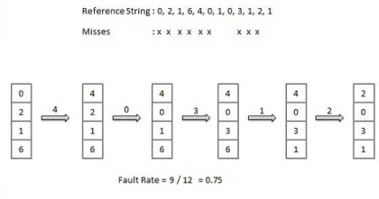
First In First out (FIFO) algorithm
Oldest page in main memory is the one which will be selected for replacement.
Easy to implement, keep a list, replace pages from the tail and add new pages at the head.
|
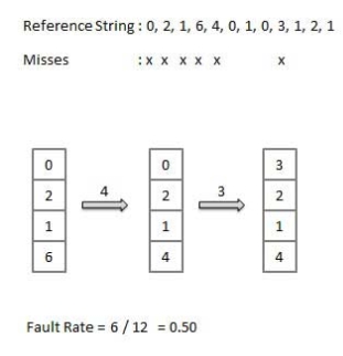
Optimal Page algorithm
An optimal page-replacement algorithm has the lowest page-fault rate of all algorithms. An optimal page-replacement algorithm exists, and has been called OPT or MIN.
Replace the page that will not be used for the longest period of time. Use the time when a page is to be used.
|
Least Recently Used (LRU) algorithm
Page which has not been used for the longest time in main memory is the one which will be selected for replacement.
Easy to implement, keep a list, replace pages by looking back into time.
|
Page buffering algorithm
To get a process start quickly, keep a pool of free frames.
On page fault, select a page to be replaced.
Write the new page in the frame of free pool, mark the page table and restart the process.
Now write the dirty page out of disk and place the frame holding replaced page in free pool.
Least frequently Used (LFU) algorithm
The page with the smallest count is the one which will be selected for replacement.
This algorithm suffers from the situation in which a page is used heavily during the initial phase of a process, but then is never used again.
Most frequently Used (MFU) algorithm
This algorithm is based on the argument that the page with the smallest count was probably just brought in and has yet to be used.
Key takeaways
- A memory unit is an essential component in any digital computer since it is needed for storing programs and data.
- Typically, a memory unit can be classified into two categories:
- The memory unit that establishes direct communication with the CPU is called Main Memory. The main memory is often referred to as RAM (Random Access Memory).
- The memory units that provide backup storage are called Auxiliary Memory. For instance, magnetic disks and magnetic tapes are the most commonly used auxiliary memories.
- Apart from the basic classifications of a memory unit, the memory hierarchy consists all of the storage devices available in a computer system ranging from the slow but high-capacity auxiliary memory to relatively faster main memory.
Paging with Example
In Operating Systems, Paging is a storage mechanism used to retrieve processes from the secondary storage into the main memory in the form of pages.
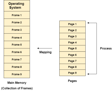
The main idea behind the paging is to divide each process in the form of pages. The main memory will also be divided in the form of frames.
One page of the process is to be stored in one of the frames of the memory. The pages can be stored at the different locations of the memory but the priority is always to find the contiguous frames or holes.
Pages of the process are brought into the main memory only when they are required otherwise they reside in the secondary storage.
Different operating system defines different frame sizes. The sizes of each frame must be equal. Considering the fact that the pages are mapped to the frames in Paging, page size needs to be as same as frame size.
|
Figure 9 - Mapping
Example
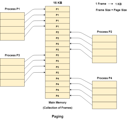
Let us consider the main memory size 16 Kb and Frame size is 1 KB therefore the main memory will be divided into the collection of 16 frames of 1 KB each.
There are 4 processes in the system that is P1, P2, P3 and P4 of 4 KB each. Each process is divided into pages of 1 KB each so that one page can be stored in one frame.
Initially, all the frames are empty therefore pages of the processes will get stored in the contiguous way.
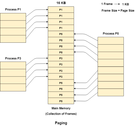
Frames, pages and the mapping between the two is shown in the image below.
|
Figure 10 - Paging
Let us consider that, P2 and P4 are moved to waiting state after some time. Now, 8 frames become empty and therefore other pages can be loaded in that empty place. The process P5 of size 8 KB (8 pages) is waiting inside the ready queue.
Given the fact that, we have 8 non contiguous frames available in the memory and paging provides the flexibility of storing the process at the different places. Therefore, we can load the pages of process P5 in the place of P2 and P4.
|
Figure 11 - Example
Memory Management Unit
The purpose of Memory Management Unit (MMU) is to convert the logical address into the physical address. The logical address is the address generated by the CPU for every page while the physical address is the actual address of the frame where each page will be stored.
When a page is to be accessed by the CPU by using the logical address, the operating system needs to obtain the physical address to access that page physically.
The logical address has two parts.
Page Number
Offset
Memory management unit of OS needs to convert the page number to the frame number.
Example
Considering the above image, let's say that the CPU demands 10th word of 4th page of process P3. Since the page number 4 of process P1 gets stored at frame number 9 therefore the 10th word of 9th frame will be returned as the physical address.
Segmentation
In Operating Systems, Segmentation is a memory management technique in which, the memory is divided into the variable size parts. Each part is known as segment which can be allocated to a process.
The details about each segment are stored in a table called as segment table. Segment table is stored in one (or many) of the segments.
Segment table contains mainly two information about segment:
Base: It is the base address of the segment
Limit: It is the length of the segment.
Why Segmentation is required?
Till now, we were using Paging as our main memory management technique. Paging is more close to Operating system rather than the User. It divides all the process into the form of pages regardless of the fact that a process can have some relative parts of functions which needs to be loaded in the same page.
Operating system doesn't care about the User's view of the process. It may divide the same function into different pages and those pages may or may not be loaded at the same time into the memory. It decreases the efficiency of the system.
It is better to have segmentation which divides the process into the segments. Each segment contain same type of functions such as main function can be included in one segment and the library functions can be included in the other segment,
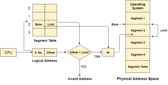
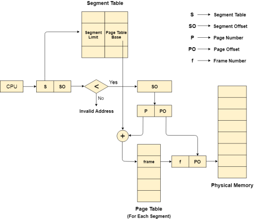
Translation of Logical address into physical address by segment table
CPU generates a logical address which contains two parts:
Segment Number
Offset
The Segment number is mapped to the segment table. The limit of the respective segment is compared with the offset. If the offset is less than the limit then the address is valid otherwise it throws an error as the address is invalid.
In the case of valid address, the base address of the segment is added to the offset to get the physical address of actual word in the main memory.
|
Figure 12 - Flowchart
Advantages of Segmentation
No internal fragmentation
Average Segment Size is larger than the actual page size.
Less overhead
It is easier to relocate segments than entire address space.
The segment table is of lesser size as compare to the page table in paging.
Disadvantages
It can have external fragmentation.
it is difficult to allocate contiguous memory to variable sized partition.
Costly memory management algorithms.
Paging VS Segmentation
Sr No. | Paging | Segmentation |
1 | Non-Contiguous memory allocation | Non-contiguous memory allocation |
2 | Paging divides program into fixed size pages. | Segmentation divides program into variable size segments. |
3 | OS is responsible | Compiler is responsible. |
4 | Paging is faster than segmentation | Segmentation is slower than paging |
5 | Paging is closer to Operating System | Segmentation is closer to User |
6 | It suffers from internal fragmentation | It suffers from external fragmentation |
7 | There is no external fragmentation | There is no external fragmentation |
8 | Logical address is divided into page number and page offset | Logical address is divided into segment number and segment offset |
9 | Page table is used to maintain the page information. | Segment Table maintains the segment information |
10 | Page table entry has the frame number and some flag bits to represent details about pages. | Segment table entry has the base address of the segment and some protection bits for the segments. |
Segmented Paging
Pure segmentation is not very popular and not being used in many of the operating systems. However, Segmentation can be combined with Paging to get the best features out of both the techniques.
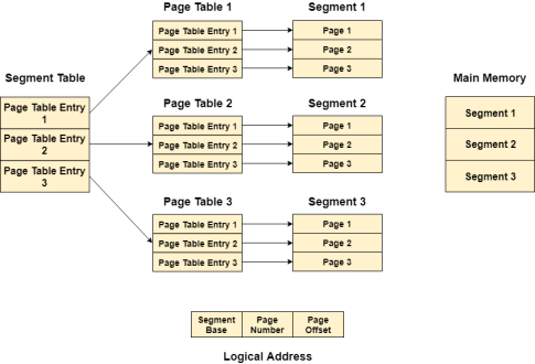
In Segmented Paging, the main memory is divided into variable size segments which are further divided into fixed size pages.
Pages are smaller than segments.
Each Segment has a page table which means every program has multiple page tables.
The logical address is represented as Segment Number (base address), Page number and page offset.
Segment Number → It points to the appropriate Segment Number.
Page Number → It Points to the exact page within the segment
Page Offset → Used as an offset within the page frame
Each Page table contains the various information about every page of the segment. The Segment Table contains the information about every segment. Each segment table entry points to a page table entry and every page table entry is mapped to one of the page within a segment.
|
Figure 14 – Logical address
Translation of logical address to physical address
The CPU generates a logical address which is divided into two parts: Segment Number and Segment Offset. The Segment Offset must be less than the segment limit. Offset is further divided into Page number and Page Offset. To map the exact page number in the page table, the page number is added into the page table base.
The actual frame number with the page offset is mapped to the main memory to get the desired word in the page of the certain segment of the process.
|
Figure 15 – Segment table
Advantages of Segmented Paging
It reduces memory usage.
Page table size is limited by the segment size.
Segment table has only one entry corresponding to one actual segment.
External Fragmentation is not there.
It simplifies memory allocation.
Disadvantages of Segmented Paging
Internal Fragmentation will be there.
The complexity level will be much higher as compare to paging.
Page Tables need to be contiguously stored in the memory.
Input-Output Interface
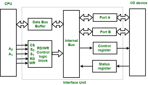
1. Data Bus Buffer
2. Read/Write Control Logic
3. Port A, Port B register
4. Control and Status register
|
Figure 16 – Interface Unit
These are explained as following below.
Data Bus Buffer :
The bus buffer use bi-directional data bus to communicate with CPU. All control word data and status information between interface unit and CPU are transferred through data bus.
Port A and Port B :
Port A and Port B are used to transfer data between Input-Output device and Interface Unit. Each port consist of bi-directional data input buffer and bi-directional data output buffer. Interface unit connect directly with an input device and output disk or with device that require both input and output through Port A and Port B i.e. modem, external hard-drive, magnetic disk.
Control and Status Register :
CPU gives control information to control register on basis of control information. Interface unit control input and output operation between CPU and input-output device. Bits which are present in status register are used for checking of status conditions. Status register indicate status of data register, port A, port B and also record error that may be occur during transfer of data.
Read/Write Control Logic :
This block generates necessary control signals for overall device operations. All commands from CPU are accepted through this block. It also allow status of interface unit to be transferred onto data bus through this block accept CS, read and write control signal from system bus and S0 , S1 from system address bus. Read and Write signal are used to define direction of data transfer over data bus.
Read Operation: CPU <---- I/O device
Write Operation: CPU ----> I/O device
The read signal direct data transfer from interface unit to CPU and write signal direct data transfer from CPU to interface unit through data bus.
Address bus is used to select to interface unit. Two least significant lines of address bus ( A0 , A1 ) are connected to select lines S0, S1. This two select input lines are used to select any one of four registers in interface unit. The selection of interface unit is according to the following criteria :
Read state :
Chip Select | Operation | Select lines | Selection of
Interface unit | ||
CS | Read | Write | S | S | |
0 | 0 | 1 | 0 | 0 | Port A |
0 | 0 | 1 | 0 | 1 | Port B |
0 | 0 | 1 | 1 | 0 | Control Register |
0 | 0 | 1 | 1 | 1 | Status Register |
Write State :
Chip Select | Operation | Select lines | Selection of | ||
CS | Read | Write | S | S | |
0 | 1 | 0 | 0 | 0 | Port A |
0 | 1 | 0 | 0 | 1 | Port B |
0 | 1 | 0 | 1 | 0 | Control Register |
0 | 1 | 0 | 1 | 1 | Status Register |
Example :
If S0, S1 = 0 1, then Port B data register is selected for data transfer between CPU and I/O device.
If S0, S1 = 1 0, then Control register is selected and store the control information send by the CPU.
Key takeaways
- In Operating Systems, Paging is a storage mechanism used to retrieve processes from the secondary storage into the main memory in the form of pages.
- The main idea behind the paging is to divide each process in the form of pages. The main memory will also be divided in the form of frames.
- One page of the process is to be stored in one of the frames of the memory. The pages can be stored at the different locations of the memory but the priority is always to find the contiguous frames or holes.
- Pages of the process are brought into the main memory only when they are required otherwise they reside in the secondary storage.
- Different operating system defines different frame sizes. The sizes of each frame must be equal. Considering the fact that the pages are mapped to the frames in Paging, page size needs to be as same as frame size.
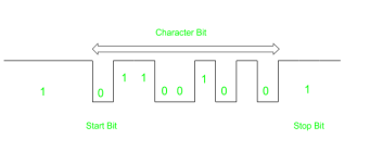
In most computer asynchronous mode of data transfer is used in which two component have a different clock. Data transfer can occur between data in two ways serial and parallel. In case of parallel multiple lines are used to send a single bit whereas in serial transfer each bit is send one at a time. To tell other devices when the character/data will be given a concept of start and end bit is used. A start bit is denoted by 0 and stop bit is detected when line return to 1-state at least one time, here 1-state means that there is not data transfer is occurring.
When a character is not being sent then line is kept in state 1. Start of character is detected when a 0 is sent. The character bit always come after 0 bit. After last bit is sent the state of line to become 1.
The diagram below shows this concept:
|
Figure 17 - Asynchronous mode
Here earlier state of line was 1 when a character has to be send a 0 is send and character bit are transferred.
Difference between serial and parallel transfer –
Serial | Parallel |
Require single line to send data | Require multiple line |
Less error and simple model | Error prone and complex working |
Economical | Expensive |
Slower data transfer | Faster data transfer |
Used for long distance | used for short distance |
Example: Computer to Computer | Example: Computer to Printer |
Asynchronous input output synchronization
Asynchronous input output is a form of input output processing that allows others devices to do processing before the transmission or data transfer is done.
Problem faced in asynchronous input output synchronization –
It is not sure that the data on the data bus is fresh or not as their no time slot for sending or receiving data.
This problem is solved by following mechanism:
Strobe
Handshaking
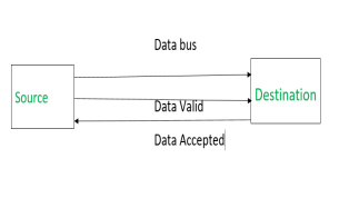
Data is transferred from source to destination through data bus in between.
1. Strobe Mechanism:
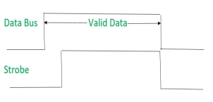
Source initiated Strobe – When source initiates the process of data transfer. Strobe is just a signal.
|
(i) First, source puts data on the data bus and ON the strobe signal.
(ii) Destination on seeing the ON signal of strobe, read data from the data bus.
(iii) After reading data from the data bus by destination, strobe gets OFF.
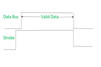
Signals can be seen as:
|
It shows that first data is put on the data bus and then strobe signal gets active.
Destination initiated signal – When destination initiates the process of data transfer.
|
(i) First, the destination ON the strobe signal to ensure the source to put the fresh data on the data bus.
(ii) Source on seeing the ON signal puts fresh data on the data bus.
(iii) Destination reads the data from the data bus and strobe gets OFF signal.
Signals can be seen as:
|
It shows that first strobe signal gets active then data is put on the data bus.
Problems faced in Strobe based asynchronous input output –
In Source initiated Strobe, it is assumed that destination has read the data from the data bus but their is no surety.
In Destination initiated Strobe, it is assumed that source has put the data on the data bus but their is no surety.
This problem is overcome by Handshaking.
2. Handshaking Mechanism:
Source initiated Handshaking – When source initiates the data transfer process. It consists of signals:
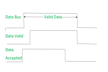
DATA VALID: if ON tells data on the data bus is valid otherwise invalid.
DATA ACCEPTED: if ON tells data is accepted otherwise not accepted.
|
(i) Source places data on the data bus and enable Data valid signal.
(ii) Destination accepts data from the data bus and enable Data accepted signal.
(iii) After this, disable Data valid signal means data on data bus is invalid now.
(iv) Disable Data accepted signal and the process ends.
Now there is surety that destination has read the data from the data bus through data accepted signal.
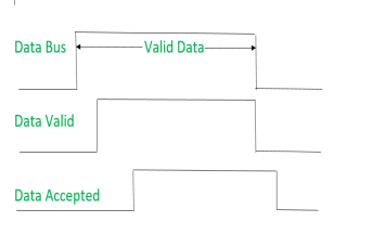
Signals can be seen as:
|
It shows that first data is put on the data bus then data valid signal gets active and then data accepted signal gets active. After accepting the data, first data valid signal gets off then data accepted signal gets off.
Destination initiated Handshaking – When destination initiates the process of data transfer.
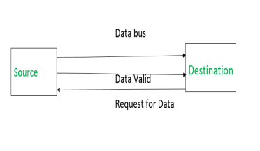
REQUEST FOR DATA: if ON requests for putting data on the data bus.
DATA VALID: if ON tells data is valid on the data bus otherwise invalid data
|
(i) When destination is ready to receive data, Request for Data signal gets activated.
(ii) source in response puts data on the data bus and enabled Data valid signal.
(iii) Destination then accepts data from the data bus and after accepting data, disabled Request for Data signal.
(iv) At last, Data valid signal gets disabled means data on the data bus is no more valid data.
Now there is surety that source has put the data on the data bus through data valid signal.
Signals can be seen as:
|
It shows that first Request for Data signal gets active then data is put on data bus then Data valid signal gets active. After reading data, first Request for Data signal gets off then Data valid signal.
Key takeaways
- In most computer asynchronous mode of data transfer is used in which two component have a different clock. Data transfer can occur between data in two ways serial and parallel. In case of parallel multiple lines are used to send a single bit whereas in serial transfer each bit is send one at a time. To tell other devices when the character/data will be given a concept of start and end bit is used. A start bit is denoted by 0 and stop bit is detected when line return to 1-state at least one time, here 1-state means that there is not data transfer is occurring.
- When a character is not being sent then line is kept in state 1. Start of character is detected when a 0 is sent. The character bit always come after 0 bit. After last bit is sent the state of line to become 1.
The method that is used to transfer information between internal storage and external I/O devices is known as I/O interface. The CPU is interfaced using special communication links by the peripherals connected to any computer system. These communication links are used to resolve the differences between CPU and peripheral. There exists special hardware components between CPU and peripherals to supervise and synchronize all the input and output transfers that are called interface units.
Mode of Transfer:
The binary information that is received from an external device is usually stored in the memory unit. The information that is transferred from the CPU to the external device is originated from the memory unit. CPU merely processes the information but the source and target is always the memory unit. Data transfer between CPU and the I/O devices may be done in different modes.
Data transfer to and from the peripherals may be done in any of the three possible ways
Programmed I/O.
Interrupt- initiated I/O.
Direct memory access( DMA).
Now let’s discuss each mode one by one.
Programmed I/O: It is due to the result of the I/O instructions that are written in the computer program. Each data item transfer is initiated by an instruction in the program. Usually the transfer is from a CPU register and memory. In this case it requires constant monitoring by the CPU of the peripheral devices.
Example of Programmed I/O: In this case, the I/O device does not have direct access to the memory unit. A transfer from I/O device to memory requires the execution of several instructions by the CPU, including an input instruction to transfer the data from device to the CPU and store instruction to transfer the data from CPU to memory. In programmed I/O, the CPU stays in the program loop until the I/O unit indicates that it is ready for data transfer. This is a time consuming process since it needlessly keeps the CPU busy. This situation can be avoided by using an interrupt facility. This is discussed below.
Interrupt- initiated I/O: Since in the above case we saw the CPU is kept busy unnecessarily. This situation can very well be avoided by using an interrupt driven method for data transfer. By using interrupt facility and special commands to inform the interface to issue an interrupt request signal whenever data is available from any device. In the meantime the CPU can proceed for any other program execution. The interface meanwhile keeps monitoring the device. Whenever it is determined that the device is ready for data transfer it initiates an interrupt request signal to the computer. Upon detection of an external interrupt signal the CPU stops momentarily the task that it was already performing, branches to the service program to process the I/O transfer, and then return to the task it was originally performing.
Note: Both the methods programmed I/O and Interrupt-driven I/O require the active intervention of the
processor to transfer data between memory and the I/O module, and any data transfer must transverse
a path through the processor. Thus both these forms of I/O suffer from two inherent drawbacks.
The I/O transfer rate is limited by the speed with which the processor can test and service a
device.
The processor is tied up in managing an I/O transfer; a number of instructions must be executed
for each I/O transfer.
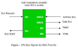
Direct Memory Access: The data transfer between a fast storage media such as magnetic disk and memory unit is limited by the speed of the CPU. Thus we can allow the peripherals directly communicate with each other using the memory buses, removing the intervention of the CPU. This type of data transfer technique is known as DMA or direct memory access. During DMA the CPU is idle and it has no control over the memory buses. The DMA controller takes over the buses to manage the transfer directly between the I/O devices and the memory unit.
|
Figure 18 – CPU bus signals for DMA Transfer
Bus Request : It is used by the DMA controller to request the CPU to relinquish the control of the buses.
Bus Grant : It is activated by the CPU to Inform the external DMA controller that the buses are in high impedance state and the requesting DMA can take control of the buses. Once the DMA has taken the control of the buses it transfers the data. This transfer can take place in many ways.
Types of DMA transfer using DMA controller:
Burst Transfer :
DMA returns the bus after complete data transfer. A register is used as a byte count,
being decremented for each byte transfer, and upon the byte count reaching zero, the DMAC will release the bus. When the DMAC operates in burst mode, the CPU is halted for the duration of the data transfer.
Steps involved are:
Bus grant request time.
Transfer the entire block of data at transfer rate of device because the device is usually slow than the
speed at which the data can be transferred to CPU.
Release the control of the bus back to CPU
So, total time taken to transfer the N bytes
= Bus grant request time + (N) * (memory transfer rate) + Bus release control time.
Where,
X µsec =data transfer time or preparation time (words/block)
Y µsec =memory cycle time or cycle time or transfer time (words/block)
% CPU idle (Blocked)=(Y/X+Y)*100 % CPU Busy=(X/X+Y)*100 |
Cyclic Stealing:
An alternative method in which DMA controller transfers one word at a time after which it must return the control of the buses to the CPU. The CPU delays its operation only for one memory cycle to allow the direct memory I/O transfer to “steal” one memory cycle.
Steps Involved are:
- Buffer the byte into the buffer
- Inform the CPU that the device has 1 byte to transfer (i.e. bus grant request)
- Transfer the byte (at system bus speed)
- Release the control of the bus back to CPU.
- Before moving on transfer next byte of data, device performs step 1 again so that bus isn’t tied up and
the transfer won’t depend upon the transfer rate of device.
So, for 1 byte of transfer of data, time taken by using cycle stealing mode (T).
= time required for bus grant + 1 bus cycle to transfer data + time required to release the bus, it will be
N x T
In cycle stealing mode we always follow pipelining concept that when one byte is getting transferred then Device is parallel preparing the next byte. “The fraction of CPU time to the data transfer time” if asked then cycle stealing mode is used.
Where,
X µsec =data transfer time or preparation time (words/block) Y µsec =memory cycle time or cycle time or transfer time (words/block) % CPU idle (Blocked) =(Y/X)*100 % CPU busy=(X/Y)*100 |
Interleaved mode: In this technique , the DMA controller takes over the system bus when the microprocessor is not using it.An alternate half cycle i.e. half cycle DMA + half cycle processor.
Key takeaway
The method that is used to transfer information between internal storage and external I/O devices is known as I/O interface. The CPU is interfaced using special communication links by the peripherals connected to any computer system. These communication links are used to resolve the differences between CPU and peripheral. There exists special hardware components between CPU and peripherals to supervise and synchronize all the input and output transfers that are called interface units.
Mode of Transfer:
The binary information that is received from an external device is usually stored in the memory unit. The information that is transferred from the CPU to the external device is originated from the memory unit. CPU merely processes the information but the source and target is always the memory unit. Data transfer between CPU and the I/O devices may be done in different modes.
Data transfer to and from the peripherals may be done in any of the three possible ways
Programmed I/O.
Interrupt- initiated I/O.
Direct memory access( DMA).
References
1 Computer system architecture by M. Morris Mano
2 Computer Architecture and parallel processing by Kai Hwang, Briggs, McGraw
3 Hill
4 Computer Architecture by Carter, Tata McGraw Hill.
5 Computer System Organization and Architecture by John D. Carpinelli, Pearson Education
