Unit-5
Power Converters
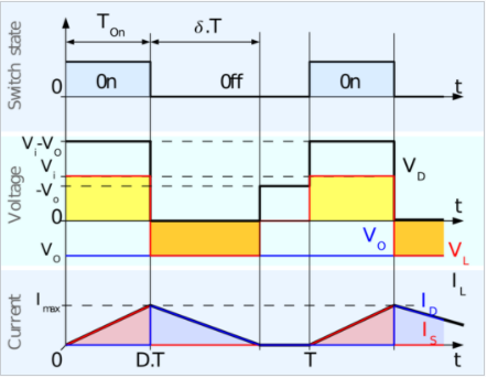
It is basically a DC-DC converter which has output either low or high than the input voltage value. It is combination of a step up (Buck) and step up (Boost) converter. These devices have a diode connected with inductor and a capacitor. The input is connected to a solid-state device. The diode acts as a switch. The circuit shown below is of a buck-boost converter.

Fig: Buck-Boost Converter
The diode is in the reverse direction to the source. The capacitor and diode are in parallel to load. We use pulse width modulation to turn the controlled switch ON and OFF. Normally time based PWM is used as frequency based is difficult in implementation. This operates in two modes
i) When switch is ON, Diode is OFF: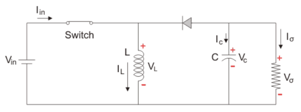
As seen from the above figure when the switch is ON it acts as a short circuit and hence, allows all the current to pass through it. In this condition the current flows through the switch and inductor and again to the input. The inductor stores energy at this time. When the switch is OFF the inductor reverses its polarity and then the current flows through the load and then diode and back to the inductor.
The total time period T = TON+TOFF
TON: ON time
TOFF: OFF time
The switching frequency fs= 1/T
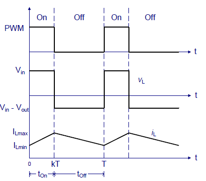
In steady state Vin=VL
VL= L  = Vin
= Vin
Now duty cycle D= 
 =
= 
At end of ON state
 ILON =
  =
=  dt =
dt = 
Ii) When switch is OFF, Diode is ON:
The circuit is shown below where the switch is in OFF state. The polarity of inductor is reversed. The current flows through the load resistance from the inductor and a step-up voltage is obtained at the output.
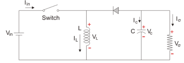
In this case VL=Vo
VL= L  = Vo
= Vo
 =
= 
TOFF= T-TON = T_DT = (1-D) T
 t= (1-D) T
 iL)open=
  (1-D) T
It is the period for which the signal is active. The time the signal takes to complete one cycle is called as period.
D= PW/T x 100%
D: Duty cycle
PW: pulse width
T: total period of signal
1-phase VSI:
The basic VSI generates ac output using semiconductor devices such as IGBT, MOSFET or BJT. The below circuit uses for pair of transistor diode acting as four switches. In case of resistive load current and voltage are in phase. In sinusoidal PWM half wave pulses are used. The width of each pulse is varied in proportion to the amplitude of sine wave.
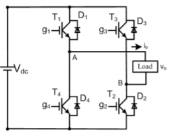
The above circuit has four switches and depending on their ON and OFF state we get the desired output. During first half of the sine wave g1 and g2 are ON the current flows through load using this path. This output holds for positive half cycle. In second half cycle g3 and g4 are ON remaining two are OFF. Now, the flow of current in this case through load is in opposite direction as in previous case.

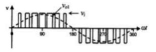
The gating pulses are generated by comparing and then applied to the switching devices.
VC= high frequency carrier wave
Vr= reference sinusoidal wave
Vo1=fundamental component of output voltage frequency
This technique is used to reduce the harmonic content of output voltage. In SPWM technique, the carrier signal is a high frequency triangular wave and it is compared with the reference sinusoidal signal. By comparing, the gating pulses are generated which are then applied to the switching devices.
3-phase VSI:
It converts DC input into 3-phase ac output. The three-phase circuit is shown below.
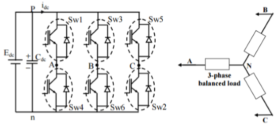
The inverter can be divided into two types due to conduction time of thyristors as:
i) 120-degree mode of operation:
In this case at a time two thyristors are ON. They remain ON for 120o and then OFF. The A side is connected to positive and B to negative end. The phase voltages are equal to line voltages.
VAB=V
VBC=-V/2
VCA=-V/2
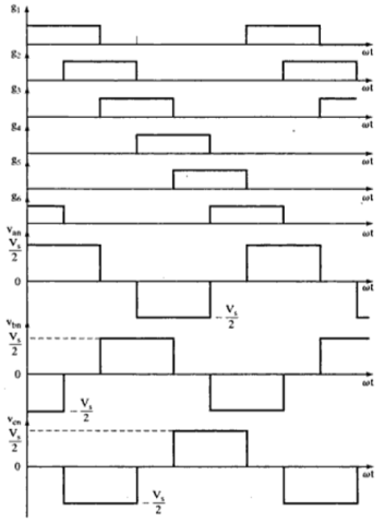
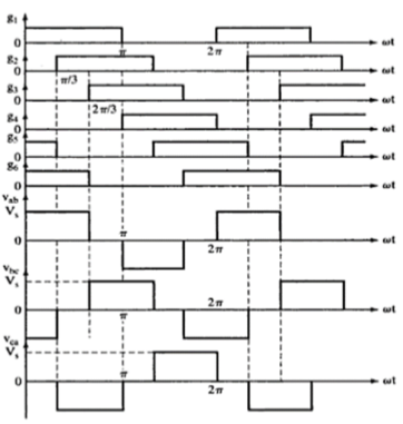
Ii) 180o mode of operation: The devices here are conducting for 180o and are switched ON at 60o interval. The terminals of bridge A, B and C are connected to the three-phase star or delta of load.
For 0-60 S1, S5 and S6 will conduct. The terminals A and C are connected to positive of source and B is connected to negative of source. The load voltages will be
VAN=V/3
VBN=-2V/3
VCN=V/3
The line voltages are
VAB=VAN-VBN= V
VBC=VBN-VCN= -V
VCA=VCN-VAN= 0
