MODULE 2
SEMICONDUCTORS
Semiconductors
Semiconductors are materials which have conductivity between conductors and insulators.
Semiconductors can be pure elements, such as silicon or germanium, or compounds such as gallium arsenide or cadmium selenide.
They are not good conductors nor good insulators as their name “semi”-conductors.
These materials such as silicon (Si), germanium (Ge) and gallium arsenide (GaAs), have electrical properties somewhere in the middle, between those of a “conductor” and an “insulator”.
They have very few “free electrons” because their atoms are closely grouped together in a crystalline pattern called a “crystal lattice” but electrons are still able to flow, but only under special conditions.
The Band Model
Bands are formed by the closely spaced orbitals.
There are three types of bands:
1. Valance Bands: Valence band it is a group of orbitals which contain electrons in the shell. Or we can sayIt is also defined as the energy band that comprises of valence electrons present in the outermost shell of an atomic structure.
These valence electrons, when provided with sufficient energy, get changed into free electrons and moves to conduction band thereby causing conductivity.It is at a lower energy level than the conduction band in the energy level diagram.
2. Conduction Band: Conduction band is a group of empty orbitals of the shells that do not contain any electron due to their configuration making the orbitals of higher energy levels.
When the electrons pass from valance band to the conduction band these solids conduct electricity with flow of charges in the form of electrons.
3. Forbidden Energy Band: These two bands are separated by a certain amount of energy known as the forbidden energy gap. In this band not a single electron is available. It diagram it is named as Band Gap.
Let us distinguish between conductor, semiconductors and insulator on the basis of these bands.
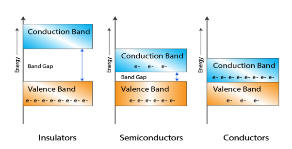
Figure 1
- In Conductors: The valance band and the conduction band overlap each other. This makes it easy for the electricity to pass through them. In conductors, the valence band is either not fully occupied with electrons, or the filled valence band overlaps with the empty conduction band. In general, both states occur at the same time, the electrons can therefore move inside the partially filled valence band or inside the two overlapping bands. In conductors there is no band gap between the valence band and conduction band.
- In Semi-conductors: there is a slight gap between the conduction band and the valance band. This band gap is less than or equal to 1.4eV. The electrons from valance shell take a little energy to excite from valance band to the conduction band.Even in semiconductors, there is a band gap, but compared to insulators it is so small that even at room temperature electrons from the valence band can be lifted into the conduction band. The electrons can move freely and act as charge carriers.
- In Insulators: In insulators the valence band is fully occupied with electrons due to the covalent bonds.To achieve conductivity, electrons from the valence band have to move into the conduction band.the energy gap is considerably large and the electrons of the valance band cannot be excited to the conduction band before the melting or the dissociation of the solid. This means that under the practically ambient condition it cannot conduct electricity.
Consider an isolated silicon atom; its energy levels are quantized. When two identical atoms are brought closer together, the quantized energy levels hybridize and split into two different levels because of the mutual interaction of the two atoms. More generally, when N atoms are moved closer, until they reach the equilibrium inter-atomic distance d, the energy levels split into N levels. These N levels are very close to each other if N is large (which is the case in a crystal) so that they eventually form a continuous energy band.
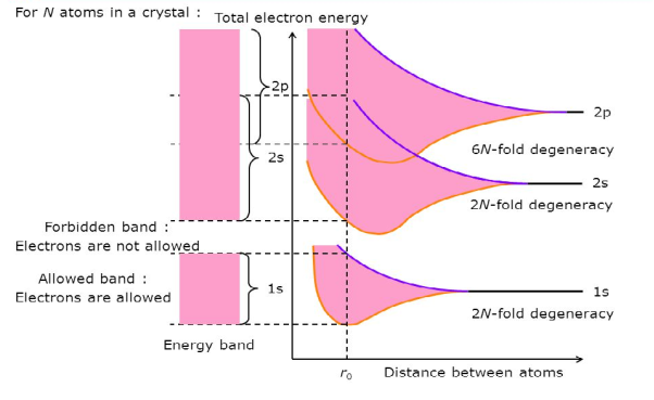
Figure 2: Formation of Energy band as a function of interatomic distance (distance between atoms)
Types of Semiconductor
There are two basic groups or classifications that can be used to define the different semiconductor types:
- Intrinsic Semiconductor
- Extrinsic Semiconductor
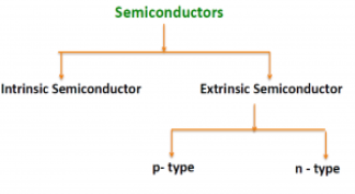
Figure 3
The semiconductor is divided into two types. One is Intrinsic Semiconductor and other is an extrinsic semiconductor. The pure form of the semiconductor is known as the intrinsic semiconductor and the semiconductor in which intentionally impurities is added for making it conductive is known as the extrinsic semiconductor.
The conductivity of the intrinsic semiconductor become zero at room temperature while the extrinsic semiconductor is very little conductive at room temperature. The detailed explanation of the two types of the semiconductor is given below.
Intrinsic Semiconductor
An intrinsic type of semiconductor material made to be very pure chemically. As a result it possesses a very low conductivity level having very few number of charge carriers, namely holes and electrons, which it possesses in equal quantities.
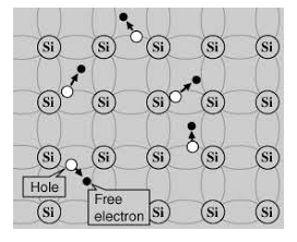
Figure 4
The most commonly used semiconductor basics material by far is silicon. Silicon has four valence electrons in its outermost shell which it shares with its neighbouring silicon atoms to form full orbital’s of eight electrons. The structure of the bond between the two silicon atoms is such that each atom shares one electron with its neighbour making the bond very stable.
As there are very few free electrons available to move around the silicon crystal, crystals of pure silicon (or germanium) are therefore good insulators. Silicon atoms are arranged in a definite symmetrical pattern making them a crystalline solid structure. A crystal of pure silica (silicon dioxide or glass) is generally said to be an intrinsic crystal (it has no impurities) and therefore has no free electrons.
An extremely pure semiconductor is called as Intrinsic Semiconductor. On the basis of the energy band phenomenon, an intrinsic semiconductor at absolute zero temperature is shown below.
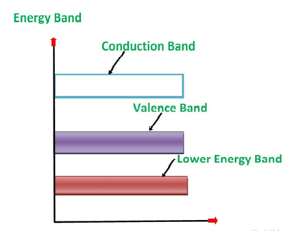
Figure 5
Its valence band is completely filled and the conduction band is completely empty. When the temperature is raised and some heat energy is supplied to it, some of the valence electrons are lifted to conduction band leaving behind holes in the valence band as shown below.
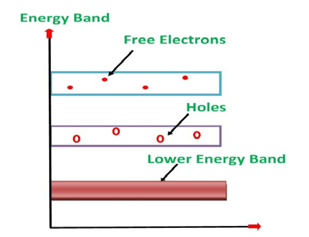
Figure 6
A hole is the absence of an electron in a particular place in an atom. Although it is not a physical particle in the same sense as an electron, a hole can be passed from atom to atom in a semiconductor material. It is considered to have positive charge. Holes are positive charge carriers.
The electrons reaching at the conduction band move randomly. The holes created in the crystal also free to move anywhere.
This behaviour of the semiconductor shows that they have a negative temperature coefficient of resistance. This means that with the increase in temperature, the resistivity of the material decreases and the conductivity increases.
But simply connecting a silicon crystal to a battery supply is not enough to extract an electric current from it. To do that we need to create a “positive” and a “negative” pole within the silicon allowing electrons and therefore electric current to flow out of the silicon. These poles are created by doping the silicon with certain impurities.
Doping
The process by which an impurity is added to a semiconductor is known as Doping. The amount and type of impurity which is to be added to a material has to be closely controlled during the preparation of extrinsic semiconductor. Generally, one impurity atom is added to a 108 atoms of a semiconductor.
The purpose of adding impurity in the semiconductor crystal is to increase the number of free electrons or holes to make it conductive.
If a Pentavalent impurity, having five valence electrons is added to a pure semiconductor a large number of free electrons will exist. Which make a n-type extrinsic semiconductor.
If a trivalent impurity having three valence electrons is added, a large number of holes will exist in the semiconductor which makes a p-type extrinsic semiconductor.
Extrinsic Semiconductor
Extrinsic types of semiconductor are those where a small amount of impurity has been added to the basic intrinsic material. This 'doping' uses an element from a different periodic table group and in this way it will either have more or less electrons in the valence band than the semiconductor itself. This creates either an excess or shortage of electrons. In this way two types of semiconductor are available: Electrons are negatively charged carriers. Holes are positively charged carriers.
Depending upon the type of impurity added the extrinsic semiconductor may be classified as n type semiconductor and p type semiconductor.
P-type Extrinsic Semiconductor
The extrinsic p-Type Semiconductor is formed when a trivalent impurity is added to a pure semiconductor in a small amount, and as a result, a large number of holes are created in it. A large number of holes are provided in the semiconductor material by the addition of trivalent impurities like Gallium and Indium. Such type of impurities which produces p-type semiconductor are known as an Acceptor Impurities because each atom of them create one hole which can accept one electron.
In a P-type semiconductor material there is a shortage of electrons, i.e. there are 'holes' in the crystal lattice. Electrons may move from one empty position to another and in this case it can be considered that the holes are moving. This can happen under the influence of a potential difference and the holes can be seen to flow in one direction resulting in an electric current flow. It is actually harder for holes to move than for free electrons to move and therefore the mobility of holes is less than that of free electrons. Holes are positively charged carriers.
A trivalent impurity like Aluminium, having three valence electrons is added to Silicon crystal in a small amount. Each atom of the impurity fits in the Silicon crystal in such a way that its three valence electrons form covalent bonds with the three surrounding Silicon atoms as shown in the figure below.
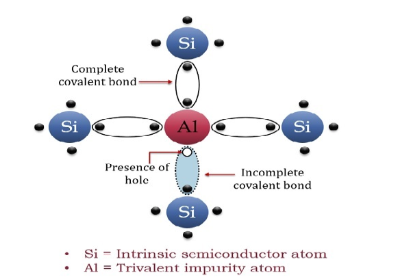
Figure 7
Energy Band Diagram of p-Type Semiconductor
The energy band diagram of a p-Type Semiconductor is shown below.
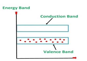
Figure 8
A large number of holes or vacant space in the covalent bond is created in the crystal with the addition of the trivalent impurity. A small or minute quantity of free electrons is also available in the conduction band.
They are produced when thermal energy at room temperature is imparted to the Silicon crystal forming electron-hole pairs. But the holes are more in number as compared to the electrons in the conduction band. It is because of the predominance of holes over electrons that the material is called as a p-type semiconductor. The word “p” stands for the positive material.
Conduction through p Type Semiconductor
In p type semiconductor large number of holes is created by the trivalent impurity. When a potential difference is applied across this type of semiconductors.
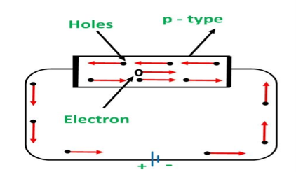
Figure 9
The holes are available in the valence band are directed towards the negative terminal. As the current flow through the crystal is by holes, which are carrier of positive charge, therefore, this type of conductivity is known as positive or p type conductivity. In a p type conductivity the valence electrons move from one covalent to another.
The conductivity of n type semiconductor is nearly double to that of p type semiconductor. The electrons available in the conduction band of the n type semiconductor are much more movable than holes available in the valence band in a p type semiconductor. The mobility of holes is poor as they are more bound to the nucleus.
Even at the room temperature the electron hole pairs are formed. These free electrons which are available in minute quantity also carry a little amount of current in the p type semiconductors.
N-typeExtrinsic Semiconductor
When a few pentavalent impurities such as Phosphoruswhose atomic number is 15, which is categorised as 2, 8 and 5. It has five valence electrons, which is added to silicon crystal. Each atom of the impurity fits in four silicon atoms as shown in the figure below.
Hence, each Arsenic atom provides one free electron in the Silicon crystal. Since an extremely small amount ofPhosphorus, impurity has a large number of atoms; it provides millions of free electrons for conduction.
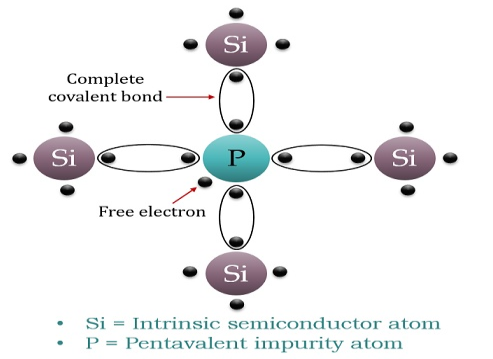
Figure 10
An N-type semiconductor material has an excess of electrons. In this way, free electrons are available within the lattices and their overall movement in one direction under the influence of a potential difference results in an electric current flow. This in an N-type semiconductor, the charge carriers are electrons.
Energy Diagram of n-Type Semiconductor
A large number of free electrons are available in the conduction band because of the addition of the Pentavalent impurity. These electrons are free electrons which did not fit in the covalent bonds of the crystal. However, a minute quantity of free electrons is available in the conduction band forming hole- electron pairs.
The Energy diagram of the n-type semiconductor is shown in the figure below.
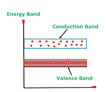
Figure 11
- The addition of pentavalent impurity results in a large number of free electrons.
- When thermal energy at room temperature is imparted to the semiconductor, a hole-electron pair is generated and as a result, a minute quantity of free electrons is available. These electrons leave behind holes in the valence band.
- Here n stands for negative material as the number of free electrons provided by the pentavalent impurity is greater than the number of holes.
Conduction through n-Type Semiconductor
In the n-type semiconductor, a large number of free electrons are available in the conduction bands which are donated by the impurity atoms. The figure below shows the conduction process of an n-type semiconductor.
When a potential difference is applied across this type of semiconductor, the free electrons are directed towards the positive terminals. It carries an electric current. As the flow of current through the crystal is constituted by free electrons which are carriers of negative charge, therefore, this type of conductivity is known as negative or n-type conductivity.
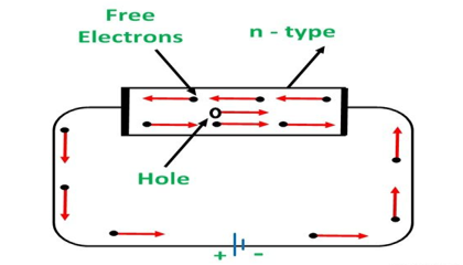
Figure 12
The electron-hole pairs are formed at room temperature. These holes which are available in small quantity in valence band also consist of a small amount of current. For practical purposes, this current is neglected.
Intrinsic semiconductors—carrier concentration
Here we will calculate the number of electrons excited into conduction band at temperature T and also the hole concentration in the valence band. It is assumed that the electrons in the conduction band behave as if they are free particles with effective mass me* and the holes near the top of the valence band behave as if they are free particles with effective mass mh*.
Here we will calculate the electron concentration, hole concentration.
Density of Electrons in Conduction Band
The number of free electrons per unit volume of semiconductor having energies in between E and E + dE is represented as N(E) dE
DE = width of Energy band
Therefore, we have:
N(E) dE = ge(E) dE fe(E) ……….(1)
ge(E) = The density of electron states per unit volume
fe(E) = Fermi-Dirac distribution function i.e. probability that an electron occupies an electron state
The number of electrons present in the conduction band per unit volume of material ‘n’ is obtained by integrating N(E) dE between the limits Ec and Ect
Where Ec = the bottom energy levels of conduction band
Ect = the bottom and top energy levels of conduction band
n =  ……….(2)
Can be written as
n =  =
= 
n =  -
-  ……….(3)
We know that above Ect, there is no electrons.
Hence, Equation (3) becomes
n =  -
- 
n =  ……….(4)
The Fermi-Dirac distribution function fe(E) can be represented as:
 (E) =
(E) = ……….(5)
Compared to the exponential value, sothe ‘1’ in the denominator can be neglected.
So >>1
>>1
Hence,  (E) =
(E) = =
=  ……….(6)
The density of electron states ge(E) in the energy space from E = 0 to E can be written as:
 (E) =
(E) =  [
[ ]3/2 (E-0) ½ ……….(7)
Where me* is the effective mass of an electron and h is Planck’s constant.
 (E)dE =
  [
[ ]3/2 (E - 0) ½dE ……….(8)
To evaluate n, the density of states is counted from Ec, since the minimum energy state in conduction band is Ec. So eq (8) can become
 (E)dE =
  [
[ ]3/2 (E - Ec) ½dE ……….(9)
Substituting Equations (6) and (9) in (4) gives
n =  3/2 (E-
 )1/2
)1/2 dE
dE
n = [
[ ]3/2
]3/2 1/2
1/2 dE ………… (10)
The above equation can be simplified by the following substitution:
Put ɛ = E − Ec ………… (11)
So, dɛ = dE
In Equation (11), Ec is constant, as we change the variable E to ε in Equation (10), the integral limits also change.
In Equation (11), as E → Ec then ε → 0 and E →∞, then ε also →∞.
The exponential term in Equation (10) becomes:
 = exp [
 ] = exp [
 ]
]
 ………… (12)
Substituting Equations (11) and (12) in (10), we get:
n = [
[ ]3/2
]3/2 dE
dE
n = [
[ ]3/2
]3/2 dE ………… (13)
Above integral (I) can be simplified by substitution. Put ε = x2
So that dɛ = 2x dx
I = 2x dx
2x dx
= dx
dx
= =
= T)3/2 ………… (14)
Substituting Equation (14) in (13) gives:
n = [
[ ]3/2
]3/2 T)3/2
T)3/2
n =
n = 
n =  ………… (15)
The term  is almost a constant compared with the exponential term as the temperature changes. So, it is a pseudo constant and is given by the symbol Nc. So, we have
n =Nc ………… (16)
Density of Holes in Valence Band
The number of holes per unit volume of semiconductor in the energy range E and E + dE in valence band is represented as P(E) dE. Proceeding same way( as in case of electrons) we have
Therefore, we have:
P(E) dE = gh(E) dE fh(E) ……….(17)
DE = width of Energy band
gh(E) = The density of holes states per unit volume
fh(E) = Fermi-Dirac distribution function i.e. probability that an hole occupies an electron state
The number of electrons present in the conduction band per unit volume of material ‘n’ is obtained by integrating P(E) dE between the limits Evb and EV
Where EV = the bottom energy levels of valence band
Evb = the bottom and top energy levels of valence band
Thetotal number of holes present in the valence band per unit volume of material ‘p’ is obtained by integrating P(E) dE
 ……….(18)
Equation (18) can be represented as:
 ……….(19)
Now we know that below Evb no holes is present. Hence, Equation (19) becomes
 ……….(20)
We know hole can also be defined as absence of an electron.
Presence of a hole = the absence of an electron
Hence, the Fermi-Dirac function of holes fh(E) in the valence band is:
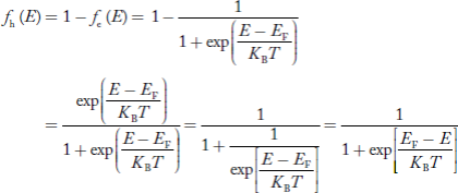
Compared to exponential, the ‘1’ in the denominator is negligible,

Hence,
 ……….(21)
The density of hole states between E and E + dE in valence band can be written similar to Equation (8.9) for electrons.
 ……….(22)
Where mh* is the effective mass of hole.
Substituting Equations (21) and (22) in (20),
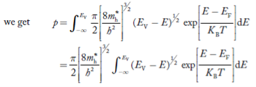 ……….(23)
The above equation can be simplified by the substitution:
Put ɛ = EV − E ............. (24)
So dɛ = −dE
In Equation (24), EV is constant, as we change the variable E to ε in Equation (23), the integral limits also change.
In Equation (24),
As E → EV then ε → 0
And E→−∞, then ε →∞
The exponential term in Equation (23) becomes:
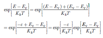 ............. (25)
Substituting Equations (24) and (25) in (23), we get:
 ………….(26)
From Equation (14), we know the integral value  T)3/2 put here and we get
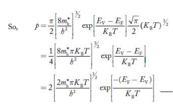 ………….(27)
….The term  is almost constant compared with the exponential term as the temperature changes. So, it is a pseudo constant and is given by the symbol NV. So, we have
 …………… (28)
Fermi Level
We know that in intrinsic semiconductor
Electron concentration ‘n’ = Hole concentration ‘p’
Equating Equations (15) and (27), we get
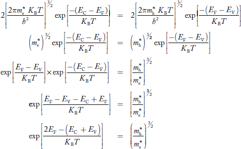
Taking logarithms on both sides, we get
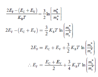 ……………… (29)
Normally, mh* is greater than me*, since ln  is very small so that EF is just lie in the middle of energy gap
Temperature effect on Fermi level
Fermi level slightly rises with increase of temperature.
But in case of pure intrinsic semiconductor like Si and Ge,
mh* ≈ me*
So in these cases Fermi level lies at the middle of energy gap.
Law of Mass Action and Intrinsic Concentration (ni)
Law of Mass Action : the product of electron and hole concentration ia a constant at a given temperature and is equal to the square of Intrinsic Concentration (ni)2 . This is called Law of Mass Action. However if impurity atoms are added to a semiconductor to increases n, there will be corresponding decrease in p such that the product np remains constant.
Thus we have np=(ni)2
- We know that electron-hole recombination take place inside a semiconductor, and also electron-hole pairs will be created due to thermal energies.
- The electron concentration and hole concentration remain constant as long as the temperature remains constant.
At temperature T K, in an intrinsic semiconductor n = p = ni,
Where ni is called intrinsic concentration.
Also the product np = ni2 ……………(30)
Substituting Equations (16) and (28) in (30) gives
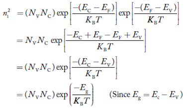
 ……………….(31)
Also substituting Equations (15) and (27) in (30) gives

 …………..(32)
If me* = mh* = m, where m is the rest mass of an electron, then Equation (32) becomes
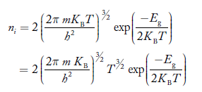
 …………..(33)
Where

For pure Ge at 300 K, the intrinsic electron concentration is about 2.4 x 10¹⁹ m-3when the concentration of germanium atoms is 4.4 x 1028 m-3. This shows that at ordinary temperature, only about two covalent bonds per 109 atoms of germanium are broken and contribute to intrinsic conductor. Whereas in metals such as copper, about 1028 electrons per cubic metre are available for conduction.
Carrier Concentration in Extrinsic Semiconductors
The number of charge carriers present per unit volume of a semiconductor material is called carrier concentration.
Suppose donor and acceptor atoms are doped in a semiconductor.
At temperatureT K,
n = number of conduction electrons
p = number of holes
N−A= number of acceptor ions
N+D = number of donor ions
We know that the below equation hold good in semiconductor. The total negative charge due to conduction electrons and acceptor ions is equal to holes and donor ions in unit volume of material.
So the material will be considered neutral if,
n + N−A = p + N+D ……….(34)
Equation(34) is called charge neutrality equation.
In the above equation
 ………..(35)
Concentration of acceptor ions N−A = acceptor concentration x probability of finding an electron in acceptor level
 ………..(36)
Similarly, the donor ions concentration is

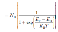 ………..(37)
In n-type material
Note
nn represents electrons in n-type material
pn represents holes concentration in n-type material.
There are no acceptor atomsso N−A = 0.
At 0 K, all the electron states in donor level are occupied by electrons.
As the temperature is increased from 0 K, some of the electrons jump from these donor states into the conduction band.
Also the concentration of holes is extremely less compared with the concentration of conduction electrons [p << n]
From Equation (34) we have
n = p N+D
(Or) n ≈ N+D …………(38) [since p << N+D]
At temperature T K,
As the temperature increase Almost all the donor atoms donate electrons to conduction band.
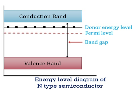
Figure 13
So, in n-type material, the free electron concentration is almost equal to the donor atoms.
So we can rewrite the above equation as
nn ≈ ND …………….(39)
Where nn represents electrons in n-type material
Also the hole concentration in n-type material can be obtained by applying law of mass action nn pn =ni2
 …………..(40)
Where pn represents holes concentration in n-type material.
In n-type material at 0 K, the Fermi energy level lies in the middle of Ec and ED

At temperature> 0K
 ……….(41)
With increase in temperature the Fermi level shifts upwards according to Equation (61) slightly due to ionization of donor atoms.
With further increase of temperature, electron-hole pairs are generated due to the breaking of covalent bonds, hence Fermi level shifts downwards.
In p-type semiconductor
Note
pp represents holes in p-type material
np represents electrons in p-type material
There are no donor atoms so means no ions present  = 0.
= 0.
At 0 K, all the acceptor levels are not occupied by electrons.
As the temperature is increased from 0 K, some electrons jump from top valence band energy levels to the acceptor states, leaving holes in the valence band and acceptor ions  are formed.
At some room temperature T K, concentration of conduction electrons is extremely less compared with hole concentration.
∴ From Equation (34), we have
n + N−A = p ……………(42)
(or) N−A ≈ p ……………. (43) [since n << N−A]
At temperature T K, in p-type material,
The hole concentration is almost equal to the acceptor atoms in unit volume of the material.
So, Equation (43) can be written as
pp ≈ NA ……………….(44)
Where pp represents holes in p-type material
The electron concentration in p-type material can be obtained by applying law of mass action as nppp = ni2
 …………….(45)
Where np represent free electron concentration in p-type material.
Figure 13
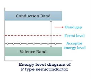
Figure 14
In p-type material, the Fermi level lies in between EV and EA at 0 K

As the temperature is increased from 0 K, the Fermi level shifts downwards slightly as per Equation (46) due to ionization of acceptor atoms.
And with further increase of temperature, electron-hole pairs are generated due to the breaking of covalent bonds, so Fermi level shifts upwards.
Carrier generation is a process where electron-hole pairs are created by exciting an electron from the valence band of the semiconductor to the conduction band, thereby creating a hole in the valence band.
Recombination is the reverse process where electrons from the conduction and holes fromvalence band recombine and are annihilated.
These processes must conserve both quantized energy and momentum, and the vibrating lattice plays a large role in conserving momentum.
- Recombination and generation are always happening in semiconductors both optically and thermally.
- Their rates are in balance at equilibrium.
- If the product of the rate becomes greater than the recombination rate, again driving the system back towards equilibrium.
- As the electron and hole densities is a constant at equilibrium, maintained by recombination and generation occurring at equal rates.
- When there is a surplus of carriers the rate of recombination becomes greater than the rate of generation, driving the system back towards equilibrium.
In semiconductors several different processes exist which lead to recombination, the most important ones are:
1) Band-to-band recombination
2) Auger generation/recombination
3) Surface recombination
1) Band-to-band recombination or Radiative recombination
Band-to-band recombination or Radiative recombination is the reverse process of photon absorption, where an electron drops back down to its equilibrium energy band and radiates a photon.
It is the process of electrons jumping down from the conduction band to the valence band in a radiative manner.
During band-to-band recombination the energy absorbed by a material is released in the form of photons. Generally these released photons contain the same or less energy than those initially absorbed.
The photon emitted may have the energy of the band gap difference or less, depending on how much energy is lost in the mechanism
Radiative recombination plays a more major role in direct band semiconductors.
The total radiative recombination rate, given below as R, is proportional to the product of the concentration of occupied states (electrons, n) in the conduction band and that of the unoccupied states in the valence band (holes, p)
R= Bnp
Band-to-band recombination depends on the density of available electrons and holes. Both carrier types need to be available in the recombination process. Therefore, the rate is expected to be proportional to the product of n and p. Also, in thermal equilibrium, the recombination rate must equal the generation rate since there is no net recombination or generation. As the product of n and p equals ni2 in thermal equilibrium, the net recombination rate can be expressed as:
U= B(np-ni2)
WhereB is the bimolecular recombination constant for a given semiconductor. It can be calculated from the semiconductor’s absorption coefficient. ni2 is the familiar “intrinsic carrier concentration”
Auger recombination
Auger recombination involves three particles: an electron and a hole, which recombines in a band-to-band transition and gives off the resulting energy to another electron or hole. The expression for the net recombination rate is therefore similar to that of band-to-band recombination but includes the density of the electrons or holes, which receive the released energy from the electron-hole annihilation.
In other words Auger recombination the energy is given to a third carrier which is excited to a higher energy level without moving to another energy band.
After the interaction, the third carrier normally loses its excess energy to thermal vibrations. Since this process is a three-particle interaction, it is normally only significant in non-equilibrium conditions when the carrier density is very high.
Auger recombination is most important at high carrier concentrations caused by heavy doping. In silicon-based solar cells, Auger recombination limits the lifetime and ultimate efficiency.
The more heavily doped the material is, the shorter the Auger recombination lifetime.
Surface recombination
Recombination at surfaces and interfaces can have a significant impact on the behaviour of semiconductor devices.
Areas of defect, such as at the surface of solar cells where the lattice is disordered, recombination is very high.
This is because surfaces and interfaces typically contain a large number of recombination centers because of the abrupt termination of the semiconductor crystal, which leaves a large number of electrically active states.
In addition, the surfaces and interfaces are more likely to contain impurities since they are exposed during the device fabrication process.
The net recombination rate due to trap-assisted recombination and generation is given by:

The recombination is due to a two-dimensional density of traps, Nts, as the traps only exist at the surface or interface.
Understanding the impacts and the ways to limit surface recombination leads to better and more robust solar cell designs. Surface recombination is high in solar cells, but can be limited.
Drift current and diffusion currents
In case of semiconductors we observe two kinds of currents.
- Drift current
- Diffusion current
Drift current Definition:- The flow of electric current due to the motion of charge carriers under the influence of external electric field is called drift current.
When an electric field E is applied across a semiconductor material, the charge carriers attain a drift velocity vd
So drift velocity vd =μ .E
The relation between current density J and drift velocity vd is
J = Nqvd
Where N is the carrier concentration
q is the charge of electron or hole
From equations (1) and (2), we get
Jdrift = NqμE
μ is the mobility of charge carrier.
The above equation shows the general expression for drift current density. Drift current density due to electrons is
Je(drift) = neμeE
Where nis the electrons carrier concentration
Andμe is the mobility of electrons.
Drift current density due to holes is
Jh(drift) = peμhE
Where p is the carrier concentration of holes.
μhis the mobility of holes
SoTotal drift current density
Jdrift(total) = Je(drift) + Jh(drift) = neμeE +peμhE
= eE (nμe+pμh )
Diffusion current
Definition:-The flow of electric current due to the motion of charge carriers under concentration gradient is called diffusion current
Or
The motion of charge carriers from the region of higher concentration to lower concentration leads to a current called diffusion current.
Let ∆N be the excess electron concentration. Then according to Fick’s law, the rate of diffusion of charge carriers is proportional to concentration gradient
Rate of diffusion of charge ∝ -
= - D
Where D is the diffusion coefficient of charge carriers.
The negative sign indicates decrease of N with increase of x So,
The diffusion current density Jdiffuis
Jdiffu = - qD
Where q is the charge of the charge carrier
Diffusion current density due to holes is
Jdiffu (hole) =- eDh
Diffusion current density due to electrons is (as electron carry negative charge so we will get +sign here.
Jdiffu (electrons) = eDe
Jdiffu (total) = Jdiffu (hole) + Jdiffu (electrons)
Jdiffu (total) = - eDh + eDe
+ eDe
The expression for total current density due to holes is
Jh (total) =Jh(drift) +Jdiffu (hole) = peμhE- eDh
The expression for total current density due to electrons is
Je (total) =Je(drift) +Jdiffu (electrons) = neμeE+ eDe
A P-N Junction Diode is formed by doping one side of a piece of silicon with a P-type dopant (Boron) and the other side with a N-type dopant (phosphorus). Ge can be used instead of Silicon. The P-N junction diode is a two-terminal device. This is the basic construction of the P-N junction diode. It is one of the simplest semiconductor devices as it allows current to flow in only one direction.
Zero Biased Condition
In this case, no external voltage is applied to the P-N junction diode; and therefore, the electrons diffuse to the P-side and simultaneously holes diffuse towards the N-side through the junction, and then combine with each other. Due to this an electric field is generated by these charge carriers. The electric field opposes further diffusion of charged carriers so that there is no movement in the middle region. This region is known as depletion width or space charge.
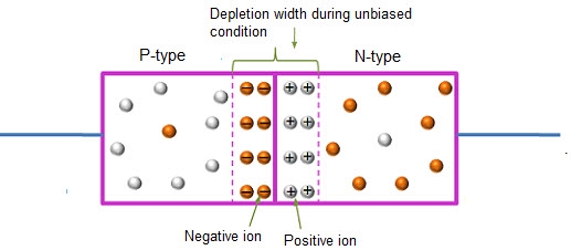
Figure 15: Unbiased or zero biased PN JunctionDiode
Forward Bias
In the forward bias condition, the positive terminal of the battery is connected to the P-Type material and the negative terminal of the battery is connected to the N-type material.This connection is also called as giving positive voltage.
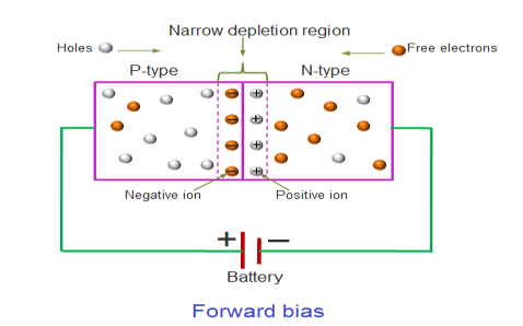
Figure 16
Electrons from the N-region cross the junction and enters the P-region. Due to the attractive force that is generated in the P-region the electrons are attracted and move towards the positive terminal. Simultaneously the holes are attracted to the negative terminal of the battery. By the movement of electrons and holes current flows. In this condition, the width of the depletion region decreases due to the reduction in the number of positive and negative ions.
If this external voltage Vf becomes greater than the value of the potential barrier, approx. 0.7 volts for silicon and 0.3 volts for germanium, the potential barriers opposition will be overcome and current will start to flow.
This is because the negative voltage pushes or repels electrons towards the junction giving them the energy to cross over and combine with the holes being pushed in the opposite direction towards the junction by the positive voltage. This results in a characteristics curve of zero current flowing up to this voltage point, called the “knee” on the static curves and then a high current flow through the diode with little increase in the external voltage as shown in I-V characteristics.
Reverse Bias
In the forward bias condition, the negative terminal of the battery is connected to the N-type material and the positive terminal of the battery is connected to the P-type material. This connection is also known as giving positive voltage. Hence, the electric field due to both the voltage and depletion layer is in the same direction. This makes the electric field stronger than before. Due to this strong electric field, electrons and holes want more energy to cross the junction so they cannot diffuse to the opposite region. Hence, there is no current flow due to the lack of movement of electrons and holes.
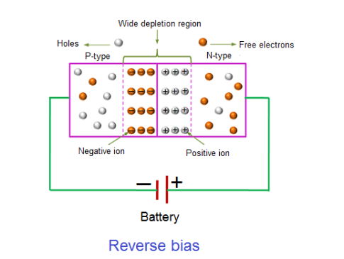
Figure 17
The positive voltage applied to the N-type material attracts electrons towards the positive electrode and away from the junction, while the holes in the P-type end are also attracted away from the junction towards the negative electrode.
The net result is that the depletion layer grows wider due to a lack of electrons and holes and presents a high impedance path, almost an insulator. The result is that a high potential barrier is created thus preventing current from flowing through the semiconductor material.
This condition represents a high resistance value to the PN junction and practically zero current flows through the junction diode with an increase in bias voltage. However, a very small leakage current does flow through the junction which can be measured in micro-amperes, ( μA ).
If the reverse bias voltage Vr applied to the diode is increased to a sufficiently high enough value, it will cause the diode’s PN junction to overheat and fail due to the avalanche effect around the junction. This may cause the diode to become shorted and will result in the flow of maximum circuit current, and this shown as a step downward slope in the reverse static characteristics curve in I-V characteristics.
I-V characteristics of PN junction diode
The I-V Characteristic Curves, which is short for Current-Voltage Characteristic Curves or simply I-V curves of an electrical device
The application of a forward biasing voltage on the junction diode results in the depletion layer becoming very thin and narrow which represents a low impedance path through the junction thereby allowing high currents to flow. The point at which this sudden increase in current takes place is represented on the static I-V characteristics curve above as the “knee” point. The current starts increasing with increase in voltage. At knee voltage current shows a sharp increment in its magnitude.This behaviour us mentioned above. As large current flow in forward biasing so we measure this current in mA.
When a junction diode is Reverse Biased,the thickness of the depletion region increases and the diode acts like an open circuit blocking current flow. So only a very small leakage current will flow.
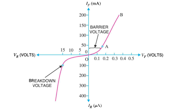 Figure 18: I-V chracteristics
As the name implies, the MS junction is that a metal and a semiconductor material are contacted closely. The metal-semiconductor (MS) contact is an important component in the performance of most semiconductor devices in the solid state.
For the ideal MS contact, several assumptions are made:
- The metal and the semiconductor are contacted intimately, which means that there is no oxide or charge layers between the contact on the atomic scale.
- No intermixing and inter diffusion between the metal and the semiconductor.
- There are no impurities at the MS interface.
The principle of forming different types of the metal-semiconductor contact is the mismatch of the Fermi energy between metal and semiconductor material, which is due to the difference in work functions.
Φ work function =Φ is defined as the energy difference between the Fermi energy and the vacuum level.
χ electron affinity= χ is defined as the required energy for moving an electron from the vacuum level to the conduction band
E0= the minimum energy needed to release an electron from the material, is used to align the metal and the semiconductor together.
The metal work function ΦM
The semiconductor work function ΦS
χ=(E0−Ec)FB|surface
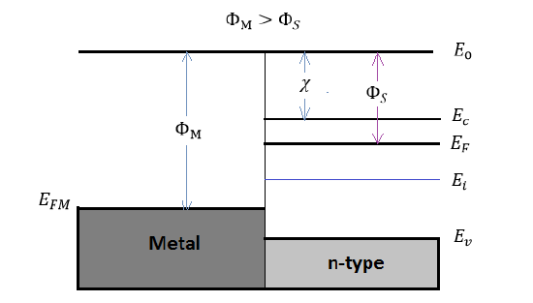
Figure 19: Energy band diagram for ideal MS contacts at an instant after contact for ΦM>ΦS and
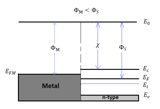
Figure 20: Energy band diagram for ideal MS contacts at an instant after contact for ΦM<ΦS
χ and Φare invariant fundamental properties that are remain unaffected by the contacting process. However, the work function of semiconductors is related with the electron affinity, the conduction band, and the Fermi energy:
ΦS=χ+(Ec−EF)FB
χ=(E0−EF)
However, the situations in Figure 19 and 20 are not in equilibrium condition, since the Fermi energy in the metal is not aligned with the Fermi energy in semiconductor ( EFS≠EFM).
Therefore, electrons will keep transferring between the semiconductor and the metal until the EF is aligned, which would cause a formation of depletion region between the MS contact. With different characteristics of the metal-semiconductor interface, two types of MS contact will be formed. We will discuss here.
There are two kinds of metal–semiconductor junction.
- Rectifying Schottky Diodes
- Non-rectifying Ohmic contact
Rectifying Schottky Diodes
The junctions between metal and lightly doped semiconductors exhibit rectifying IV- characteristics similar to those of PN junctions. They are called Schottky diodes and have some interesting applications.
Under a forward bias (VA>0)
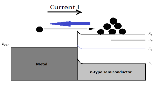
Figure 21: Energy band diagram and carrier activity at forward biasing (VA>0)
Under Reverse Biasing VA<0
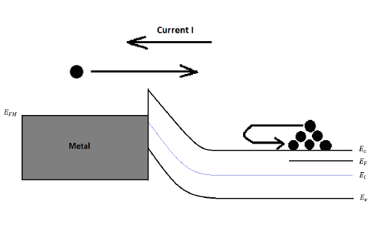
Figure 22: Energy band diagram and carrier activity at reverse biasing VA<0
I−VCharacteristics
In general, the current flowing through the Schottky contact can be defined with the applied voltage, which is very similar to those of pn-junction diode. The IVexpression is:
I=I0(eqVA/kT−1),where
I0 is a saturate current
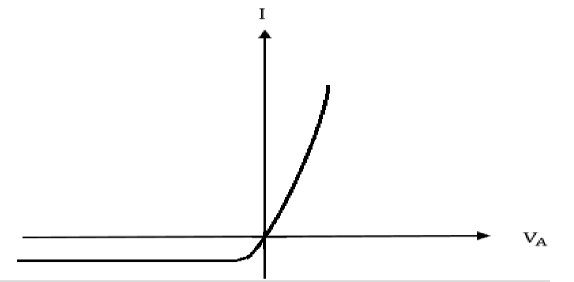
Figure 23
Non-rectifying Ohmic Contact
The junction between metal and heavily doped semiconductors behaves as low-resistance ohmic contacts (basically electrical shorts). Ohmic contacts are an important part of semiconductor devices and have a significant influence on the performance of high-speed transistors
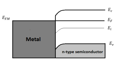
Figure 24(a) Energy band diagram under equilibrium for ΦM<ΦS
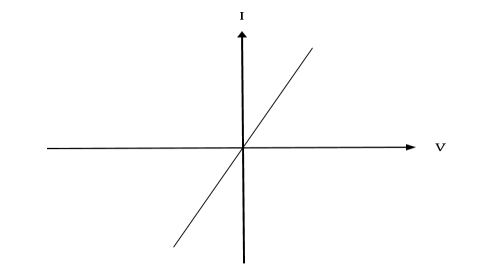
Figure 25: IV characteristics of Ohmic contact
Whenever a metal and a semiconductor are in intimate contact, there exists a potential barrier between them to stop most charge carriers (i.e. electrons or holes) to flow from one to the other. Only a small number of carriers have enough energy to get over the barrier and cross to the other material.
Points keep in mind
- Lower the barrier height
The barrier height is a property of the materials we use. We try to use materials whose barrier height is small. Annealing can create an alloy between the semiconductor and the metal at the junction, which can also lower the barrier height.
- Make the barrier very narrow
One very interesting property of very tiny particles like electrons and holes is that they can "tunnel" through barriers that they don't have enough energy to just pass over. The probability of tunnelling becomes high for extremely thin barriers (in the tens of nanometres). We make the barrier very narrow by doping it very heavily (1019 dopant atoms/cm3 or more).
When a bias is applied to the junction, it can have one of two effects: it can make the barrier appear lower from the semiconductor side, or it can make it appear higher. The bias does not change the barrier height from the metal side. The result of this is a Schottky Barrier (rectifying contact
In SchottkyBarrier (rectifying contact) the junction conducts for one bias polarity, but not the other. Almost all metal-semiconductor junctions will exhibit some of this rectifying behaviour. Schottky Contacts make good diodes, and can even be used to make a kind of transistor.
For getting signals into and out of a semiconductor device, we generally want a contact that is Ohmic. Ohmic contacts conduct the same for both polarities. (They obey Ohm's Law).There are two ways to make a metal-semiconductor contact look ohmic enough to get signals into and out of a semiconductor (or doing the opposite makes a good Schottky contact).
Unlike the majority of electronic devices, which are silicon based, optoelectronic devices are predominantly made using three to four semiconductor compounds such as GaAs, InP, GaN, and GaSb, and their alloys due to their direct-band gap.
Understanding the properties of these materials has been of vital importance in the development of optoelectronic devices. Since the first demonstration of a semiconductor laser in the early 1960s, optoelectronic devices have been produced in their millions, pervading our everyday lives in communications, computing, entertainment, lighting, and medicine. It is perhaps their use in optical-fiber communications that has had the greatest impact on humankind, enabling high-quality and inexpensive voice and data transmission across the globe.
Types of Optoelectronics Devices
Optoelectronics are classified into different types such as
- Photodiode
- Solar Cells
- Light Emitting Diodes
- Laser Diodes
- Optical Fibre
Photo Diode
Silicon photo diode is a light sensitive device. It is also called as photo detector. Photo diode converts light signals into electrical signals. It is always operated in reverse biased condition.
Symbol
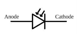
Figure 26
A photo diode is a semiconductor light sensor that generates a voltage or current when light falls on the junction. It consists of an active P-N junction, which is operated in reverse bias. When a photon with plenty of energy strikes the semiconductor, an electron or hole pair is created. The electrons diffuse to the junction to form an electric field.
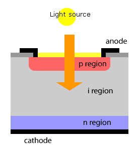
Figure 27 Photodiode
The magnitude of photo current depends on the number of charge carriers generated and on the light falling of diode element. The current is also affected by the frequency of the light falling on the diode element. The magnitude of current under large reversed bias is given by
I =Is +I0(1 + exp(V/ηVT)
WhereIs = short circuit current which is proportional to the light intensity
I0 Reverse saturation current
V Voltage across the diode
VT Volt equilent of temperature
η Parameter, 1 for Ge, 2 for Si
Applications
Photo diodes are used as
- Light detectors
- Demodulators
- Encoders
- Optical communication system
- High speed counting and switching circuits.
Solar Cells
A solar cell or photo-voltaic cell is an electronic device that directly converts sun’s energy into electricity. When sunlight falls on a solar cell, it produces both a current and a voltage to produce electric power.
Sunlight, which is composed of photons, radiates from the sun. When photons hit the silicon atoms of the solar cell, they transfer their energy to lose electrons; and then, these high-energy electron flow to an external circuit.
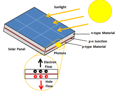
Figure 28: Solar Cell
The solar cell is composed of two layers which are struck together. The first layer is loaded with electrons, so these electrons are ready to jump from the first layer to the second layer. The second layer has some electrons taken away, and therefore, it is ready to take more electrons.
The advantages of solar cells are that, there is no fuel supply and cost problem. These are very dependable and require little maintenance.
Light emitting diode
Light emitting diode is a pn junction device. It is always operated in forward biased condition. LED converts electrical energy into light energy. In the fabrication of LED’s direct band gap semiconductors like GaP, GaAsP are used. In direct band gap semiconductors most of the energy is emitted in the form of light when hole and electron recombination takes place.
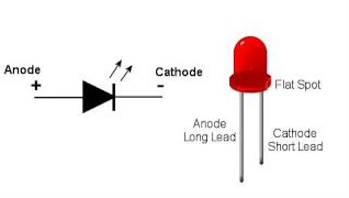
Figure 29: LED
When an LED is forward biased the electrons and holes move in towards the junction and recombination takes place. As a result of recombination the electrons lying in the conduction band of an n- region fall into the holes lying in the valence band of a p –region. The difference of energy in the valence band and conduction band is radiated in the form of light energy. Here their excess energy is transferred to the emitted photon. The brightness of emitted light is directly proportional to the forward bias current.
The usage of LED is advantageous as it consumes less power and produces less heat. LEDs last longer than incandescent lamps.
Applications LEDs are used in
- For instrument display
- In calculators
- Digital clocks
- For indicating power ON/ OFF
- For optical switching application
- In optical communication system
- Medical devices
Laser Diode
Direct band gap semiconductors are preferred in the fabrication of laser diodes because they emit energy in terms of light when an electron and hole recombination takes place. These are operated at forward biased condition. Compound semiconductors like GaAS and InP are examples for direct band gap semiconductors.
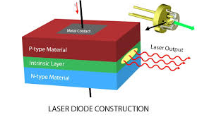
Figure 30
The semiconductor laser device is always operated in forward bias condition. Electrons and the holes are the minority charge carriers in p-region and p-region semiconductors. When a huge current (104 Amp/mm2) is passing through the p-n junction, p-region is positively biased, holes are injected into n-region from p-region and n-region is negatively biased electrons are injected into p-region from n-region
The continuous injection of charge carriers creates the population inversion of minority carriers in n and p sides’ respectively. The electrons and holes recombine and release of light energy takes place in or near the junction as shown in figure 1. The emitted photons increase the rate of recombination of injected electrons from the n-region and holes in p-region by inducing more recombinations.
For GaAs semiconductor Eg =1.4eV
From Planck’s law Eg =hc/λ
From here λ = hc/ Eg =8874Å
The wave length of emitted radiation depends up on the concentration of donor and acceptor atoms in GaAs. .In case of GaAs homo-junction which has an energy gap of 1.44eV gives a laser beam of wave length around 8874Å. The efficiency of the laser emission is increases when we cool the GaAs diode.
Optical Fibre
An optical fibre or optic fibre is a plastic and transparent fibre made of plastic or glass. It is somewhat thicker than a human hair. It can function as a light pipe or waveguide to transmit light between the two ends of the fibre.
Optical fibres usually include three concentric layers: a core, a cladding and a jacket. The core, a light transmitting region of the fibre, is the central section of the fibre, which is made of silica. Cladding, the protective layer around the core, is made of silica.This creates an optical waveguide that limits the light in the core by total reflection at the interface of the core-cladding. Jacket, the non-optical layer around the cladding, typically consists of one or more layers of a polymer that protect the silica from the physical or environmental damage.
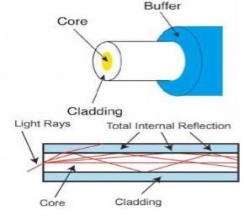
Figure 31 Optical Fibre
Along with the fibre-optic cable, jackets are available in different colour. These colours allow the recognition of the fibre-optic cable and the type of cable one is dealing with. For example, an orange-colour cable clearly indicates a single-mode fibre, while a yellow one indicates a multimodefibre. In the single-mode fibre, one mode propagates and the light rays travel straight through the cable. In a multimode cable, the light rays travel through the cable following different modes.
Application
These cables are used in telecommunications, sensors, fibre lasers, bio-medicals and in many other industries. The advantages of using optical-fibre cable include their higher bandwidth, less signal degradation, weightlessness and thinness than a copper wire, cost-effectiveness, flexibility, and hence they are used in medical and mechanical imaging systems.