MODULE 3
LIGHT-SEMICONDUCTOR INTERACTION
- In semiconductors electrons can make transitions between two energy states and generate or destroy photons in the process.
- In particular, transitions between the conduction band (EC) and the valence band ( EV) are optically active.
- As the lower conduction band generally consists of s-like states while the upper valence band contains of p-like states.
- Spontaneous emission, absorption, and stimulated emission can all take place between conduction band (EC) states and valence band (EV) states.
Absorption
- Similar to stimulated absorption in optics in the semiconductor absorption all we need is an incoming photon, a valence band energy state occupied by an electron, and an empty conduction band energy state.
- We know that in equilibrium condition, the valence band is fully occupied and the conduction band is empty.
- We know that for optical absorption between two states in an atom only occurred for a narrow spectrum of photon energies so here in optical absorption in a semiconductor can occur over a wide range of photon energies.
- This process carry out when the energy photon is greater than or equal to the band gap energy.
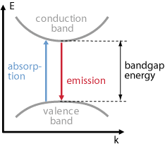
Figure 1
- Incoming photon interacts with electron in valence band and provides it sufficient energy for excitation and by getting enough energy the electron jump to conduction band and leaving hole in valence band.
- The absorption process creates an electron in the conduction band and a hole in the valence band, it is also called optical generation.
- If the electrons created at energies higher than the band edge will quickly stabilize to the lowest conduction band energy states by releasing phonons.
- Holes created deep in the valence band will ‘float up’ to the valence band edge.
Spontaneous Emission
- Consider the system is in equilibrium but temperature is increased let us consider it is at T temperature.
- Electrons and holes can be created by optical absorption and other pumping mechanisms.
- The spontaneous emission process is possible for a wide range of photon energies above the band gap similar to absorption.
- At T temperature the lowest energy states are mostly full in conduction band.
- At T temperature the highest energy states are mostly empty in valence band.
- Therefore, the spontaneous emission observed in semiconductor in which photon has energy nearly equal to the band gap energy.
- Since the spontaneous emission process ‘destroys’ an electron and a hole, it is also called spontaneous optical recombination.
Why ordinary silicon is not useful for light emission?
Why stimulated emission process is not carrying out in indirect band gap semiconductors?
Silicon has an indirect band gap. That means that the lowest energy states in the conduction band have a different momentum than the highest energy states in the valence band.
As we discussed above At T temperature the lowest energy states are mostly full in conduction band and the highest energy states are mostly empty in valence band. So these are the states that are most likely to be occupied by an electron and a hole.
The spontaneous emission process must conserve both energy and momentum, but photons carry very little momentum but it is not zero have some finite value.
Therefore, an electron at the ‘bottom’ of the conduction band is unable to recombine with a hole at the ‘top’ of the valence band via spontaneous photon emission, because that would violate conservation of momentum: the electron would have to undergo a significant momentum change, and the photon is unable to carry away enough momentum.
This is the reason ordinary silicon is not useful for light emission and stimulated emission process is not carrying out in indirect band gap semiconductors.
Stimulated emission
- The stimulated emission process ‘destroys’ an electron and a hole, it is also called stimulated optical recombination.
- In order to make stimulated emission the dominant optical process, we need to achieve population inversion.
- It is the most important process for laser operation.
- In this process a copy of the incoming photon is produced.
- We expect that in most cases the stimulated emission will occur primarily between band-edge states, as these states are most likely to be occupied with electrons and holes just like in spontaneous emission.
- Semiconductor optical amplifiers generally amplify light whose photon energy is approximately equal to the band gap energy of the semiconductor gain medium.
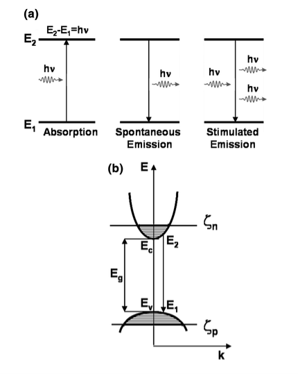
Figure 2
Let us calculate the joint density of states for both the conduction band and valence band of low-dimensional systems.
We know that inter band transitions occur between the two due to the absorption and emission of light.
Here we will combine conduction band and valence band density-of-states to get joint density of states
Joint density of states will represents the absorption spectrum of the material.
We will find that it is proportional to the system’s absorption coefficient α.
Let us therefore call the initial valence band k -value kn and the final conduction band k –value kk .The associated energy of the conduction band edge is then
Ecb =Ec+ ………..(1)
Where Ec is the bulk conduction band edge energy
me is the electron’s effective mass.
Similarly for the valence band hole, we have
Evb =Ev+ ………..(2)
Ev is the valence band edge energy
mh is the hole’s effective mass.
Now, we know that momentum is given by
p = k ………..(3)
The transition must conserve momentum That mean the total final and initial momenta are equal. We thus have
pk= pn+pphoton
 kk =
kk = kn+
kn+ kphoton ………..(4)
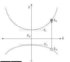
Figure 3 : Representation of the conduction and valence bands ink -space as well as a vertical transition between them upon the absorption of light.
Where pphoton represents the momentum carried by the photon. As a result,
kk =kn+kphoton ………..(5)
We will see that kk and kn for interband optical transitions are both proportional toπ/a,where “a” represents an interatomic spacing.
But here
kphoton ∝1/λ ………..(6)
Where λ is the wavelength of light.
We know that wavelength of light is greater than interatomic spacing i.e. λ>>a
And we find that
kk =kn
This is why optical transitions between the valence band and conduction band in
k -space are often said to be vertical.
By using this information an expression for the optical transition energy is obtain, and from which we will obtain a relationship between k and E given below
E = Ecb - Evb = (Ec –Ev) + +
+  )………..(7)
Eg = the band gap
It is basically the energy difference between the conduction band edge and the valence band energy, representing as
Eg= (Ec –Ev) ………..(8)
Also we have seen from the conservation of momentum that
kk=kn =k
This result in
E = Eg + +
+  ) ………..(9)
Where the reduced mass is defined as
 =
= +
+  ………..(10)
The desired bulk density is g(E) = )3/2
)3/2 –
–  )1/2 ………..(11)
Which depend on square root of energy.
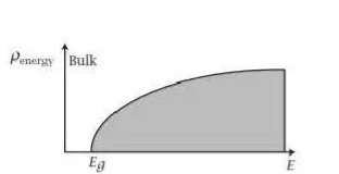
Figure 4: the pictorial representation of joint density of states
The behaviour of a collection of photons depends upon the distribution of energy among the photons. Let us first elaborate the term Distribution of Energy.
The distribution of a fixed amount of energy among a number of identical particles depends upon the density of available energy states and the probability that a given state will be occupied.
Distribution functiongives the probability that a given energy state will be occupied.
Let us suppose if there are more available energy states in a given energy interval, then probability for that energy interval will be high as compared to other interval.
n(E )∆E = g(E)f(E)∆E
n(E ) = number of particles per unit volume between energy interval E and E+∆E
g(E) = Density of Energy state =number of states per unit volume between energy interval E and E+∆E
∆E = Energy interval
f(E) = Distribution Function = probability that a particle is in energy state E
Since photons are bosons, the distribution function is the Bose Einstein Distribution Function.
f(E) =
Where the normalization constant A=1 for photons.
This distribution determines the probability that a given energy state will be occupied, but must be multiplied by the density of states function to weight the probability by the number of states available at a given energy.
Electromagnetic standing waves in a cavity at equilibrium with its surroundings cannot take just any path. They must satisfy the wave equation in three dimensions

Quantum mechanically the amplitude of the wave must be zero at the walls. If the value of amplitude is non-zero that mean there would be dissipation of energy and violate our supposition of equilibrium..
The reflection path around the cavity is such that it must produce a standing wave.
By using boundary conditions the solution of the wave isof the form

Substituting this solution into the wave equation above gives

Which simplifies to

|
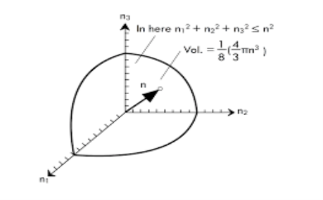
Figure 5: The Rayleigh scheme for counting modes.
Treating the "quantum numbers" n as a space such that a given set of n values determines a point in that space,
The number of possible states is proportional to the "volume" in "n-space".
It is convenient to define a radius R in n-space

Using the photon energy

The energy can be expressed in terms of R.

The n-space associated with the standing wave solutions involves only positive values of n, so the volume must be divided by 8.
Because of two planes of polarization for photons it must be multiplied by 2 . The number of values is then

The number of states per unit volume is

The final density of states as a function of energy can be obtained by deriviative of this population with respect to energy.

This represents the number of photons per unit volume per unit energy at energy E. Note that the result is independent of the dimension L showing that the expression can be applied to a region of space at equilibrium.
The density of states in terms of frequency or wavelength can be obtained by expressing the number of states per unit volume in terms of frequency or wavelength. Upon solving the equation we will come with the following results.

Fermi’s Golden provides one way to calculate the transition rate between two certain quantum mechanically defined states. Transition is from one Eigen state to other Eigen state.
Transition rate is transition probability per second
The Fermi golden rule can be used for calculating the transition probability rate for an electron that is excited by a photon from the valence band to the conduction band in a direct band-gap semiconductor, and also for when the electron recombines with the hole and emits a photon
Consider a quantum mechanical system with a Hamiltonian  0.
0.
The set of eigen states|n of the Hamiltonian satisfy
 0|n=n|n
Suppose now at t=0 a time dependent perturbation, described by
{ +e-it +
 -eit}
-eit}
The total Hamiltanion for t0 is,
 =
=  0+
0+ +e-it +
 -eit
-eit
 0 =unperturbed Hamiltonian and
{ +e-it +
 -eit} is perturbed Hamiltonian
The time dependent part is responsible for transitions between states, and the rates for these transitions is given by Fermi's Golden Rule.
For the Hamiltonian to be Hermitian, Hamiltonian must satisfy the condition of hermitian as given below.
 + =
+ = -)+
-)+
Let us Suppose at t=0 the an electron was sitting in energy eigen state|k
For t0 the state of the electron is changed and it is given by

Where

The quantity |cn(t)|2 gives the probability of the electron being in state |n
We put the above expression for|(t) in the time-dependent Schrodinger equation,

And take the bra on both sides with|k to get
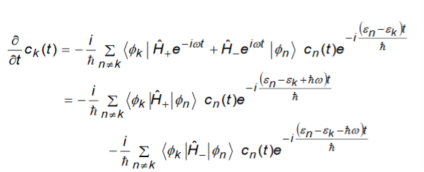
……………..(1)
Some terms of the right hand side of the above equation are resonant and important where as some are not resonant and are not important.
The resonant terms are those for which the time dependent exponentials are close to zero and for which the energy n differs from the energy kby values close ℏ.
These terms don’t oscillate rapidly as a function of time and therefore give much larger contribution to the sum than the non-resonant terms.
We remove all the non-resonant terms and assume that the summation on the right hand side is only over the resonant terms.
This means that for each n at most only one term on the right hand side will contribute (but never both).
Next we write a similar equation for cn(t) (nk) assuming it is a coefficient of one of the resonant terms.

Note that on the right hand side we have retained only one term because
ck(t0) 1and all other coefficients are approximately zero for t0.
We directly integrate Equation (2) and get

Since the time exponentials are rapidly varying functions of time compared to ck(t’).we can pullck(t’) out of the integral and then integrate to get

Depending on the relative energy alignment of levels n and k only one term (which is resonant) on the right hand side will contribute in a significant way (but never both). We keep only that term and then substitute the result into Equation (1) taking care to keep only the resonant terms. This gives

Now to figure out the transition rate we need to evaluate |ck(t)|2/t. This can be obtained by taking the above equation, multiplying on both sides by ck*(t), and then adding its complex conjugate to it to obtain,
For times that are large the two sin functions, as a functions of ℏ, become very sharply peaked at the energy differences k-n and n-k, and may be approximated as delta functions with a total integrated weight equal to . We finally have
|ck(t)|2/t = |ck(t)|2
The above equation shows that the probability of the electron being in the initial state decays exponentially with time because the electron is likely to make a transition to another state. The probability decay rate is given by

Here two terms involve and both have their own significance.
- The first part is due to transitions from the initial state |k to all final states whose energy is smaller than the energy of the initial state by ℏ.
- The second part is due to transitions from the initial state |k to all final states whose energy is larger than the energy of the initial state by ℏ.
Fermi's golden rule states that
Transition rate to states of higher energy is given as

Transition rate to states of lower energy is given as

In each case, upward or downward transitions, the final states are those that are connected to initial state by the matrix elements

In these transitions, the energy conservation is imposed by the delta functions. Additional selection rules related to the matrix element.
Optical Loss and Gain
Optical gain is the most important requirement for the understanding of a semiconductor laser because it describes the optical amplification in the semiconductor material. This optical gain is due to stimulated emission associated with light emission created by recombination of electrons and holes.
The phenomenon of electron-photon interaction has two components:
1) The emission of photons due to the recombination of electrons from the conduction band with the holes in the valence band
2) The reverse transition causing the absorption of photons.
Photon emission has again two components:
1) The Spontaneous Emission
2) The Stimulated Emission
- In absorption, the conduction band is mostly empty, while the valence band is mostly full, so that we may assume that fc( Eck )≈ 0, and fv( Evk )≈1 .
- But the absorption process is found to be stronger than the emission process.
- Emission process dominates over the absorption process in case of lasers
- The density of the carriers, both electrons and holes, is made large by the injection process.
- The Fermi functions fc(Eck) for electrons in the conduction band is no longer zero but has a large value.
- Also, the function fv( Evk) for electrons in the valence band has a value different from unity.
- The emission and absorption rates are required forthe calculation of the laser gain.
- The gain coefficient g is the difference of the emission and the absorption rate.
- It is obtained by changing the sign of the absorption coefficient.
- The absorption coefficient α(1/cm)in the crystal is the fraction of photons absorbed per unit distance.
α = 
Where S is the optical intensity i.e. the injected number of photons per unit area per second  energy of a photon
- With the help of Einstein coefficient and optical interaction phenomena we can formulate the general equation for optical gain and absorption coefficient.
Optical gain in semiconductor lasers describes the optical amplification of the semiconductor material which is due to the stimulated emission associated with light emission created by recombination of electrons and holes.
Optical losses are due to light which could have generated an electron-hole pair but it does not because the light is reflected from the front surface or not absorbed in the solar cell.
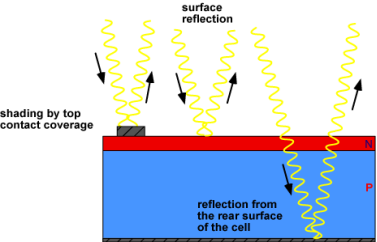
Figure 6: Sources of optical loss in a solar cell
- Top contact coverage of the cell surface can be minimised although this may result in increased series resistance.
- Anti-reflection coatings can be used on the top surface of the cell.
- Reflection can be reduced by surface texturing.
- The solar cell can be made thickerto increase absorption (although light that is absorbed more than a diffusion length from the junction has a low collection probability and will not contribute to the short circuit current).
- The optical path length in the solar cell may be increased by a combination of surface texturing and light trapping.
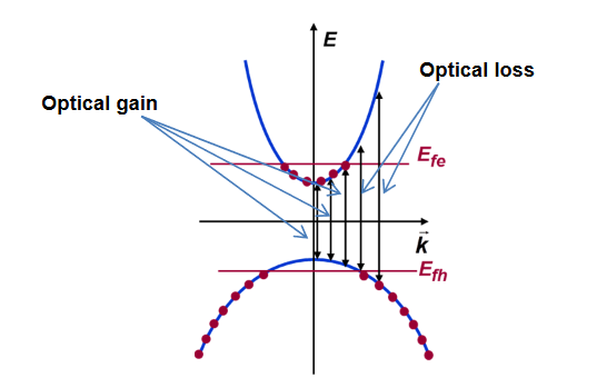
Figure 7
Given a value for the Fermi level splitting, optical frequencies for which Eg experience optical gain and frequencies for which
  ,
, experience optical loss.
Eg is the condition for population inversion and can be realized if, for example, electrons are removed from the valence band and placed in the conduction band, as shown in the Figure above.
Note that for the situation shown in the Figure, optical gain ()<0 will be experienced by radiation with frequency in the range Eg , but radiation with frequency in the range
 ,
, will experience optical loss()>0.
Photovoltaic effect
The photovoltaic effect is the generation of a voltage due to optical excitations when a semiconductor is illuminated at the electrodes or at internal barriers or p-n junctions.
The voltage developed when a semiconductor body containing a p-n junction is exposed to optical illumination.
Following Two effects are possible.
Transverse Photovoltaic Effect
When one ohmic contact is on the p-region and the second ohmic contact is on the n-region of the body. This is known as the transverse photovoltaic effect. The transverse photovoltaic effect is commonly used in photodiodes, radiation detectors, tracking detectors and solar energy converters etc.
Lateral Photovoltaic Effect when both contacts are on the same type of material either on p-type or n-type. This is known as lateral photovoltaic effect. Nowadays the lateral photovoltaic effect is used as the radiation tracking transducer.
For most applications, the devices are operated in the steady state condition with the radiation continuously falling on the devices
Photovoltaic effect process occurs when two dissimilar materials in close contact produce an electrical voltage when struck by light.
The photovoltaic effect occurs in solar cells. These solar cells are composed of two different types of semiconductors - a p-type and an n-type - that are joined together to create a p-n junction When a light photon with sufficient energy hits an atom in this region, it throws out an electron. The electron, now free to move, travels through the n-type semiconductor to metal contacts on the surface. The hole left by the absence of the electron travels in the opposite direction, through the p-type semiconductor. By joining these two types of semiconductors, an electric field is formed in the region of the junction. This field causes negatively charged particles to move in one direction and positively charged particles in the other direction.
Light striking crystals such as silicon or germanium, in which electrons are usually not free to move from atom to atom within the crystal, provides the energy needed to free some electrons from their bound condition. Free electrons cross the junction between two dissimilar crystals more easily in one direction than in the other, giving one side of the junction a negative charge and, therefore, a negative voltage with respect to the other side, just as one electrode of a battery has a negative voltage with respect to the other. The photovoltaic effect can continue to provide voltage and current as long as light continues to fall on the two materials. This current can be used to measure the brightness of the incident light or as a source of power in an electrical circuit, as in a solar power system.
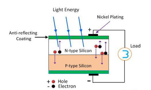
Figure 8
The Photovoltaic Effect
When unexcited, electrons hold the semiconducting material together by forming bonds with surrounding atoms, and thus they cannot move. However in their excited state in the conduction band, these electrons are free to move through the material. Because of the electric field that exists as a result of the p-n junction, electrons and holes move in the opposite direction as expected. Instead of being attracted to the p-side, the freed electron tends to move to the n-side. This motion of the electron creates an electric current in the cell. Once the electron moves, there's a "hole" that is left. This hole can also move, but in the opposite direction to the p-side. It is this process which creates a current in the cell.
Exciton
They were first proposed in 1931 by a guy named Yakov Frenkel. He actually was describing something observed by H. H. Poole involving conduction in insulators. In fact, Frenkel introduced the idea of a hole into the physics vernacular and certain types of holes are still known as Frenkel defects.
In crystals of insulators and semiconductors, when an incident photon is absorbed by electron it gets excited from the valence to the conduction band thus a positive charged vacancy i.e. hole is created in the valence band. The attractive Coulomb interaction exists between the excited electron and the hole. This force binds them together to form a bound neutral compound system of the two charge carriers such as a hydrogen atom. Such a bound system of a pair of charge carriers is called an exciton.
An exciton carries a crystal pseudo momentum which is equal to the vector sum of the individual momenta of the electron and individual momenta of the hole and their relative momentum.
Pseudo momentum (crystal) = momenta of the electron + momenta of the hole+ relative momentum.
Whereas the pseudomomentum enables an exciton to move throughout a crystal and the relative momentum determines its internal structure.
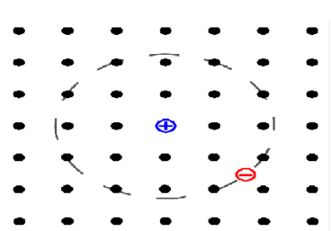
Figure 9
Because of the attractive Coulomb interaction between the electron and the hole in an exciton, the internal exciton states are analogous to those of a hydrogen atom and some of the lower energy states lie below the conduction band by an energy equivalent to the exciton binding energy in that state.
In a perfect crystal the motion of an exciton is uniform, but this can be slowed down by the presence of crystal imperfections such as vacancies, impurities, and structural disorders.
The imperfections can trap or dissociate an exciton radiatively or nonradiatively, and the lattice vibrations (phonons) can also cause its self-trapping or dissociation.
Theory of Excitons
Theory of excitons was first formulated by Frenkeland subsequently developed by Peierls and Wannier. There are two approaches for deriving the energy eigenvalues and Eigen functions of excitons.
1. Frenkel Excitons or For Tightly Bound
- This is observed in materials with a relatively small dielectric constant.
- The coulomb interaction between an electron and a hole may be strong and the excitons thus tend to be small almost of the size of the unit cell.
- Molecular excitons entirely located on the same molecule.
- It has binding energy of the order of 0.1 to 1 eV.
- Frenkel excitons are typically found in alkali halide in inorganic crystals and in organic molecular crystals composed of aromatic molecules such as anthracene and tetracene.
- Frenkel exciton also observes in transition metal compounds with partially-filled d-shells. This includes on-site d-d excitations
- Absorption of a photon resonant with a d-d transition leads to the creation of an electron-hole pair on a single atomic site which can be treated as a frenkel exciton.
2. Wannier excitons orfor weakly bound
- It is also called the large radii orbital excitons.
- Wannier-Mott excitons are typically found in semiconductor crystals with small energy gaps and high dielectric constants, but have also been identified in liquidssuch as liquid xenon. They are also known as large excitons.
- The Coulomb interaction are less between electrons and holes which result in large radius than the lattice spacing. The result is in Wannier excitons small effective mass of electrons also favours large exciton radii.
- Because of the lower masses and the screened Coulomb interaction, the binding energy is usually much less than that of a hydrogen atom, typically on the order of 0.01eV.
- In single-wall carbon nanotubes, excitons have both Wannier-Mott and Frenkel character. This is due to the nature of the Coulomb interaction between electrons and holes in one-dimension. The dielectric function of the nanotube itself is large enough to allow for the spatial extent of the wave function to extend over a few to several nanometers along the tube axis, while poor screening in the vacuum or dielectric environment outside of the nanotube allows for large (0.4 to 1.0eV) binding energies.
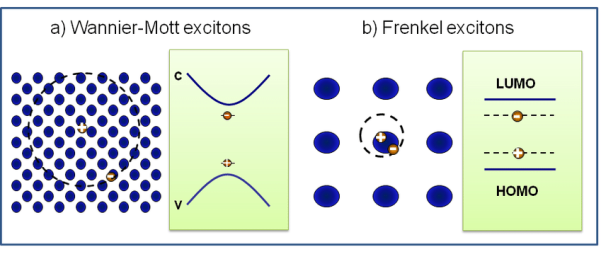
Figure 10: Wannier-Mott and Frenkel excitons
This is given by Paul Drude in 1900. The Drude model provides a classical mechanics approach to describing conductivity in metals.This theory gives electrical and thermal conduction in a metal.
Assumptions of the Drude Model
Assumptions of drude model iare given below.
- Electrons in a metal behave much like particles in an ideal gas
- It is consider as there is no Coulombic interaction and no collisions between particles. This is called the independent electron approximation.
- Positive charges are located on immobile ions. The electrons do not experience coulombic interaction with the ions, but they do collide with the ions and can change direction and velocity.
- Electrons attain thermal equilibrium due collisions with the ions.
- Their mean kinetic energy within the lattice at equilibrium is given below

Where
me = The mass of an electron
T = Temperature in Kelvin
vT =The Average Velocity at a given temperature T
kB = Boltzmann constant
The average velocity vT is about 105 m/s.
- The average distance of an electron’s free movement between collisions is called the mean free path. It is represented by λ. For metals, the mean free path is typically estimated as 1 nm
- τ is mean life time also known as the relaxation time . The mean time τ between collisions can be calculated by using the equation
τ=λ/vT
Theory
Let us suppose n is the conduction electron density. It is defined as the number of free electrons per volume. It is the density of the gas formed by the free electrons.
The conduction electron density is calculated by assuming that each atom contributes ZV conducting electrons. ZV represents the number of outer shell electrons for metal atoms in the ionic lattice. The conduction electron density is

Where ρm is density in kg/m3
M is the atomic mass in kg per atom
Let us suppose that the average time for a collision-free drift τ, the average drift velocity of an electron in a metal can be calculated using the equation below.
Here, e represents the charge of an electron in Coulombs and ℇ is electromotive force in volts (a vector quantity).

Where, e is the charge of an electron in Coulombs
ℇ is electromotive force in volts. It is a vector quantity.
We know that the number of electrons passing through a given area per unit time Je

The amount of charge passing through a given area per unit time Jc are given below. Where, n is the number of electrons.

The current density j is calculated by the equation below.

This can be used to derive the following expression, which is equivalent to Ohm’s law V=IR.

From here we can easily calculate the conductivity σ and the resistivity ρ are given by the equations below.

The mobility μ of an electron in a lattice is given below. The mobility can be interpreted as the ratio of the drift velocity to the applied electric field.

Using mobility, conductivity and resistivity can be calculated by alternative formulas.

The Drude Model and Optical Reflectivity of Metals
Light can be described as an electromagnetic wave in the form of a transverse plane.
The electric field for light in the propagating in the z direction is given by the equation below.

Where ℇ0 is the amplitude in the xy plane of the wave,
λ0 is the wavelength in a vacuum,
n is the index of refraction,
Andκ is a parameter that gives attenuation of the light’s intensity inside the given material.
In other words the equation for the electric field of light propagating in the z direction can be expressed using the dielectric constant of the given material.

An electron within the electric field from an electromagnetic wave moves according to the following equation of motion .this can be derived from newton’s law F=ma.

Note –e is electric charge whereas e-iωt is exponential term.
Solving the differential equation above gives the following result.

As a result of the electric field from the electromagnetic wave, the electron undergoes displaced in a periodic manner. This leads to a changing dipole moment given by
–ex(t)
We know that dipole moment is eqiual to the product of charge and distance between charges.
We know that Dielectric functions describe the permittivity of given media over time. Permittivity is the amount of charge needed to generate a single unit of electric flux within the medium. Using the above results and some other known formulas, the dielectric function for a material can be derived.

By setting a parameter ωP2 equal to ne2/meε0, the dielectric function can be rewritten as below. Note that ωP is called the plasma frequency.

- For ω<ωP, the value of ε is real and negative, making the square root of ε purely imaginary. As such, the light does not transmit into the metal in this case. Since energy is conserved, the light is reflected instead.
- For ω>ωP, the value of ε is real and positive. As such, the light does propagate into the metal in this case.
- Metals reflect low-frequency light and are transparent for high-frequency light. The transition occurs at the plasma frequency ωP.
- The plasma frequency can be measured experimentally or calculated using the conduction electron density n.
The Drude Model and the Wiedemann-Franz Law
The Wiedemann-Franz law states that, for any metal at a given temperature, the ratio of thermal conductivity κ to electrical conductivity σ is a constant L. Furthermore, L is proportional to temperature as temperature varies. L is called the Lorenz number.

Thermal conductivity is defined by the equation below

Where Q is the amount of heat transferred per time t
k is the thermal conductivity constant for a given material
A is the area of cross-sectional
d is the thickness of the given material
ΔT is the difference in temperature across the material.
Above mentioned formula is for one dimensional.
The ideal gas-related equations from the Drude model can be used to generate an equivalent formula for LT.

In spite of some minor inconsistencies with experimental data, this theoretical calculation often gives strikingly accurate results.
Limitations of Drude Model
- The Drude model does not take into account collisions between electrons themselves.
- It also does not consider electrostatic interactions between the electrons and the lattice ions.
- The Drude model cannot explain the conductivity of alloys. Even small impurities can drastically decrease the conductivity of metals in a way which is not predicted by the Drude model.
- As mentioned, the Drude model underestimates conductivity of metals at low temperatures. This is because the assumption of a constant mean free path based on atomic spacing is incorrect. The mean free path varies greatly with temperature.
- Electrons cannot be treated as classical particles since they have substantial wave character under the conditions of the Drude model.
- From a classical mechanics perspective, the electrons should contribute greatly to the heat capacity of metals. But this result does not agree with experimental data.