MODULE 5
ENGINEERED SEMICONDUCTOR MATERIALS
The density of states function describes the number of states that are available in a system and is essential for determining the carrier concentrations and energy distributions of carriers within a semiconductor.
In semiconductors, the free motion of carriers is limited to two, one, and zero spatial dimensions. When applying semiconductor statistics to systems of these dimensions, the density of states in quantum wells (2D), quantum wires (1D), and quantum dots (0D) must be known.
Density of state of two-Dimensional Structures (quantum wires)
We can model a semiconductor as an infinite quantum well (2D) with sides of length L. Electrons of mass m* are confined in the well.
If we set the potential energy in the well to zero, solving the Schrödinger equation yields

 ………………1

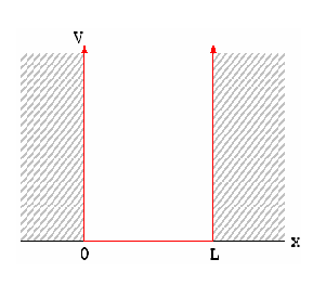
Figure 1
Using separation of variables, the wave function becomes
 ………………2
Substituting Eq. 2 into Eq. 1 and dividing through by xyyields

Where k= constant
This makes the equation valid for all possible x and y terms only if terms including x (x) and y (y) are individually equal to a constant.
Thus,

Where


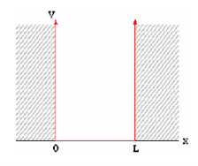
Figure 2
The solutions to the wave equation where V(x) = 0 are sine and cosine functions

Since the wave function equals zero at the infinite barriers of the well, only the sine function is valid. Thus, only the following values are possible for the wave number (k):

Recalling from the density of states 3D derivation…
k-space volume of single state cube in k-space:

V is the volume of the crystal. Vsingle-state is the smallest unit in k-space and is required to hold a single electron.
k-space volume of sphere in k-space
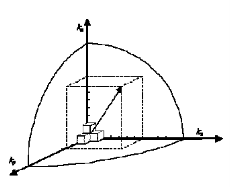
Figure 3


Recalling from the density of states 3D derivation…
k-space volume of single state cube ink-space:

k-space volume of sphere ink-space:

Number of filled states in a sphere:

A factor of two is added to account for the two possible electron spins of each solution.
Correction factor for redundancy in counting identical states +/- nx, +/-ny, +/-nz

For calculating the density of states for a 2D structure (i.e. quantum well), we can use a similar approach, the previous equations change to the following:
k-space volume of single state cube in k-space:

k-space volume of sphere in k-space:

Number of filled states in a sphere:


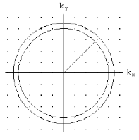
Figure 4
So we get the value of N

Substituting

We get

The density per unit energy is then obtained using the chain rule:

The density of states per unit volume, per unit energy is found by dividing by V (volume of the crystal).
g(E)2D becomes:

As stated initially for the electron mass, m m*.
m*.
Thus,
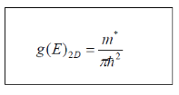
It is significant that the 2D density of states does not depend on energy. Immediately, as the top of the energy-gap is reached, there is significant number of available states.
Density of state of one-Dimensional Structures (quantum wires)
For calculating the density of states for a 1D structure (i.e. quantum wire), we can use a similar approach. The previous equations change to the following:

k-space volume of single state cube in k-space:

k-space volume of sphere in k-space:


Number of filled states in a sphere:

Continued…..

Substituting

We get

Upon Rearranging we get

The density per unit energy is then obtained by using the chain rule:

The density of states per unit volume, per unit energy is found by dividing by V (volume of the crystal).
g(E)1D becomes:

Simplifying yields…


As stated initially for the electron mass, m m*. Also, because potential energy is zero so Energy term we have here is only kinetic energy, So it is considered E
 Ec.
Ec.
Thus,

Density of state of zero-Dimensional Structures (quantum dots)
When considering the density of states for a 0D structure (i.e. quantum dot), no free motion is possible. Because there is no k-space to be filled with electrons and all available states exist only at discrete energies, we describe the density of states for 0D with the delta function.
Thus,

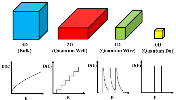
Figure 5: Density of state
Low-Dimensional Structures
When one or more of the dimensions of a solid are reduced sufficiently, its physicochemical characteristics notably depart from those of the bulk solid. With reduction in size, novel electrical, mechanical, chemical, magnetic, and optical properties can be introduced. The resulting structure is then called a low-dimensional structure (or system). The confinement of particles, usually electrons or holes, to a low- dimensional structure leads to a dramatic change in their behaviour and to the manifestation of size effects that usually fall into the category of quantum-size effects.
The low dimensional materials exhibit new physicochemical properties not shown by the corresponding large-scale structures of the same composition. Nanostructures constitute a bridge between molecules and bulk materials. Suitable control of the properties and responses of nanostructures can lead to new devices and technologies.
Classification of Low-dimensional Materials
Low-dimensional structures are usually classified according to the number of reduced dimensions they have. More precisely, the dimensionality refers to the number of degrees of freedom in the particle momentum. Accordingly, depending on the dimensionality, the following classification is made:
Three-dimensional (3D) structure or bulk structure: No quantization of the particle motion occurs, i.e., the particle is free.
Two-dimensional (2D) structure or quantum well: Quantization of the particle motion occurs in one direction, while the particle is free to move in the other two directions.
One-dimensional (1D) structure or quantum wire: Quantization occurs in two directions, leading to free movement along only one direction.
Zero-dimensional (0D) Structure or quantum dot (sometimes called “quantum box”): Quantization occurs in all three directions.
Two-Dimensional Structures: Quantum Wells
In a 2D structure, particles are confined to a thin sheet of thickness Lz along the z axis by infinite potential barriers that create a quantum well, as illustrated in the below figure.
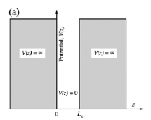
Figure 6
A particle cannot escape from the quantum well 0 z
z L z and loses no energy on colliding with its walls z=0 and z=Lz. In real systems, this confinement is due to electrostatic potentials (generated by external electrodes, doping, strain, impurities, etc.), the presence of interfaces between different materials (e.g., in core-shell nanocrystals), the presence of surfaces (e.g., semiconductor nanocrystals), or a combination of these agents. Motion of the particle in the other two directions (i.e., in the xy plane) inside the quantum well is free. It is generally accepted that quantum confinement of electrons by the potential wells of nanometer-sized structures provides one of the most powerful and versatile means to control the electrical, optical, magnetic, and thermoelectric properties of solid state functional materials. A 1D potential profile for electrons can be physically implemented by using two heterojunctions. The below figure shows a quantum well structure.
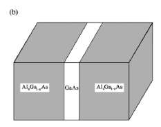
Figure 7
A GaAs Quantum well inserted between two AluGa1-uAs as barrier layers. The layer of GaAs is a quantum well because the barrier layers are made of a material with a larger bandgap than GaAs; the energy difference between the valence band and conduction band in a semiconductor is called the bandgap. By adjusting the aluminium content of the barrier layers and the thickness of the GaAs layer at the time of growth, quantum wells with electronic properties tailored to the user’s specifications can be created. This practice is referred to as quantum engineering.
The infinitely deep 1D potential well is the simplest confinement potential to treat in quantum mechanics. In classical mechanics, the solution to the problem is trivial, since the particle will move in a straight line and always at the same speed until it reflects from a wall at an equal but opposite angle. However, in order to find the quantum-mechanical solution, many fundamental concepts need to be introduced.
One-Dimensional Structures: Quantum Wire
A standard quantum well layer can be patterned with photolithography or perhaps electron-beam lithography, and etched to leave a free standing strip of quantum well material; the latter may or may not be filled in with an overgrowth of the barrier material (in this case, Ga(1-x)AlxAs). Any charge carriers are still confined along the heterostructure growth (z-) axis, as they were in the quantum well, but in addition (provided the strip is narrow enough) they are now confined along an additional direction, either the x- or the y-axis, depending on the lithography.
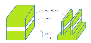
Figure 8
The following Figure shows an expanded view of a single quantum wire, where clearly the electron (or hole) is free to move in only one direction, in this case along the y-axis.
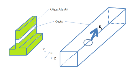
Figure 9
Zero-Dimensional Structures: Quantum Dot
Quantum dots can again be formed by further lithography and etching, e.g. If a quantum well sample is etched to leave pillars rather than wires, then a charge carrier can become confined in all three dimensions, as shown in Figure.
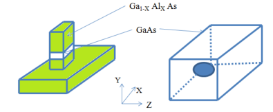
Figure 10
A quantum dot is a semiconductor nanostructure that confines the motion of conduction band electrons, valence band holes, or excitons (bound pairs of conduction band electrons and valence band holes) in all three spatial directions.
The confinement can be due to electrostatic potentials (generated by external electrodes, doping, strain, impurities), the presence of an interface between different semiconductor materials (e.g. In core-shell nanocrystal systems), the presence of the semiconductor surface (e.g. Semiconductor nanocrystal), or a combination of these.
A quantum dot has a discrete quantized energy spectrum.
The corresponding wave functions are spatially localized within the quantum dot, but extend over many periods of the crystal lattice.
A quantum dot contains a small finite number (of the order of 1-100) of conduction band electrons, valence band holes, or excitons, i.e., a finite number of elementary electric charges.
Small quantum dots, such as colloidal semiconductor nanocrystals, can be as small as 2 to 10 nanometers, corresponding to 10 to 50 atoms in diameter and a total of 100 to 100,000 atoms within the quantum dot volume.
Self-assembled quantum dots are typically between 10 and 50 nm in size.
Quantum dots defined by lithographically patterned gate electrodes, or by etching on two-dimensional electron gases in semiconductor heterostructures can have lateral dimensions exceeding 100 nm.
At 10 nm in diameter, nearly 3 million quantum dots could be lined up end to end and fit within the width of a human thumb.
Characterization Techniques
Electron microscope techniques provide very powerful tools to investigate nanometer scaled structures in solids, especially by using high resolution electron microscopy (HREM) and conventional transmission electron microscopy (TEM). The present overview describes the possibilities of investigating quantum dot(QD) structures by TEM and HREM. EM/HREM image interpretation requires a theoretical structure modelling and the subsequent simulation of image contrast in order to understand the obtained features and to provide contrast rules.
There are many zero‐dimensional (0D) nanostructures, such as nanoparticles, nanoclusters, nanocrystals, and quantum dots in different terms. 0D nanostructures are the simplest building block that may be used for designing and constructing 1D, 2D, and complex 3D nanostructures, and nanodevices. QDs’ size is generally calculated using conventional techniques like scanning electron microscopy (SEM), transmission electron microscopy (TEM),Atomic-force microscopy (AFM). XRD is also used to determine the characteristics of low dimensional material. We will discuss all these technique one by one.
Scanning Electron Microscopy (SEM)
The high resolution scanning electron microscope is a versatile tool for nanotechnology and advanced materials science, moreover, opens up new dimensions in archaeology, biology, earth science, meteorite research, hydrology and many other research areas.
Principle
In this technique, an electron beam is focused onto sample surface kept in a vacuum by electro-magnetic lenses (since electron possesses dual nature with properties of both particle and wave, hence an electron beam can be focused or condensed like an ordinary light). The beam is then scanned over the surface of the sample. The scattered electron from the sample is then fed to the detector and then to a cathode ray tube through an amplifier, where the images are formed, which gives the information of the sample
Instrumentation
It comprises of a heated filament as a source of electron beam, condenser lenses, aperture, evacuated chamber for placing the sample, electron detector, amplifier, CRT with image forming electronics, etc.
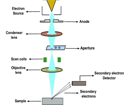
Figure 11
The SEM is an instrument that produces a largely magnified image by using electrons instead of light to form an image. A schematic diagram of the SEM is shown in Figure. A beam of electrons is produced at the top of the microscope by an electron gun. The electron beam follows a vertical path through the microscope, which is held within a vacuum chamber.
The beam travels through electromagnetic fields and lenses, which focus the beam down towards the sample. Once the beam hits the sample, electrons and X - rays are ejected from the sample. Detectors collect these X - rays, backscattered electrons and secondary electrons and convert them into a signal that is sent to a screen similar to a television screen. This produces the final image. In this research work, the powder samples were placed on the carbon tape which is attached to the sample holder.
The image formation in a scanning electron microscope is different from that in a conventional optical microscope. In SEM a focused mono-energetic electron beam scans the sample surface producing various "products" from the surface. These are secondary electrons, backscattered electrons and X-ray photons.
Advantages
- Advantages of a Scanning Electron Microscope include its wide-array of applications, the detailed three-dimensional and topographical imaging and the versatile information garnered from different detectors.
- SEMs are also easy to operate with the proper training and advances in computer technology and associated software make operation user-friendly.
- This instrument works fast, often completing SEI, BSE and EDS analyses in less than five minutes. In addition, the technological advances in modern SEMs allow for the generation of data in digital form.
- Although all samples must be prepared before placed in the vacuum chamber, most SEM samples require minimal preparation actions.
Disadvantages
- The disadvantages of a Scanning Electron Microscope start with the size and cost.
- SEMs are expensive, large and must be housed in an area free of any possible electric, magnetic or vibration interference.
- Maintenance involves keeping a steady voltage, currents to electromagnetic coils and circulation of cool water.
- Special training is required to operate an SEM as well as prepare samples.
- SEMs are limited to solid, inorganic samples small enough to fit inside the vacuum chamber that can handle moderate vacuum pressure.
- SEMs carry a small risk of radiation exposure associated with the electrons that scatter from beneath the sample surface.
Applications
- Scanning electron microscopy has been applied to the surface studies of metals, ceramics, polymers, composites and biological materials for both topography as well as compositional analysis.
- An extension of this technique is Electron Probe Micro Analysis (EPMA), where the emission of X-rays, from the sample surface, is studied upon exposure to a beam of high energy electrons.
- Depending on the type of detectors used this method is classified in to two as: Energy Dispersive Spectrometry (EDS) and Wavelength Dispersive Spectrometry (WDS). This technique is used extensively in the analysis of metallic and ceramic inclusions, inclusions in polymeric materials and diffusion profiles in electronic components.
Transmission Electron Microscopy (TEM)
Transmission Electron Microscopy (TEM) provides powerful techniques for understanding various information of materials at very high spatial resolution, including morphology, size distribution, crystal structure, strain, defects, chemical information down to atomic level and so on.
The transmission electron microscope is a very powerful tool for material science. A high energy beam of electrons is shone through a very thin sample, and the interactions between the electrons and the atoms can be used to observe features such as the crystal structure and features in the structure like dislocations and grain boundaries. Chemical analysis can also be performed. TEM can be used to study the growth of layers, their composition and defects in semiconductors. High resolution can be used to analyze the quality, shape, size and density of quantum wells, wires and dots.
All the information that TEM can give to us are from electron-sample interaction. The transmitted electrons that have passed through the thin sample are detected to form images, which is the reason to call it “transmission” electron microscopy.
In order to allow electronsto transmit through the sample, TEM sample must be very thin typically; sample thickness is less than 200 nm,depending on the compositionof sampleand the expected information from TEM characterization.
The TEM operates on the same basic principles as the light microscope but uses electrons instead of light. Because the wavelength of electrons is much smaller than that of light, the optimal resolution attainable for TEM images is many orders of magnitude better than that from a light microscope. Thus, TEMs can reveal the finest details of internal structure - in some cases as small as individual atoms.
Working
The beam of electrons from the electron gun is focused into a small, thin, coherent beam by the use of the condenser lens. This beam is restricted by the condenser aperture, which excludes high angle electrons. The beam then strikes the specimen and parts of it are transmitted depending upon the thickness and electron transparency of the specimen. This transmitted portion is focused by the objective lens into an image on phosphor screen or charge coupled device (CCD) camera. Optional objective apertures can be used to enhance the contrast by blocking out high-angle diffracted electrons. The image then passed down the column through the intermediate and projector lenses, is enlarged all the way.
The image strikes the phosphor screen and light is generated, allowing the user to see the image. The darker areas of the image represent those areas of the sample that fewer electrons are transmitted through while the lighter areas of the image represent those areas of the sample that more electrons were transmitted through.
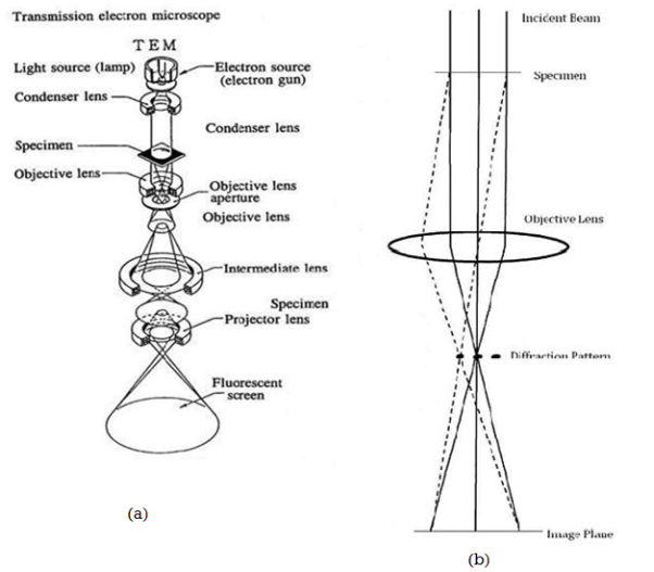
Figure 12 (a) - General layout of a TEM describing the path of electron beam in a TEM
Figure 12 (b) - A ray diagram for the diffraction mechanism in TEM
|
|
High-resolution TEM (HRTEM).The imaging mechanism of HRTEM is phase contrast, which uses the interference of the transmitted beam and diffracted beams to form images at atomic level. HRTEM is useful for the imaging of atom arrangements in projection. This technique normally requires very thin samples (less than 15 nm in thickness, as thin as possible). The interpretation of HRTEM images is always challenging.
AFM
AFM is a powerful imaging and measurement technique that has become critical to nanoscale research and to industrial R&D in all of its possible forms. A good example of this is in the semiconductor industry, where AFM is used in quality control and imaging for silicon integrated circuits.
Atomic force microscopy is arguably the most versatile and powerful microscopy technology for studying samples at nanoscale. It is versatile because an atomic force microscope can not only image in three-dimensional topography, but it also provides various types of surface measurements to the needs of scientists and engineers. It is powerful because an AFM can generate images at atomic resolution with angstrom scale resolution height information, with minimum sample preparation.
Atomic-force microscopy (AFM) is a surface scanning technique that has sub-nanometer scale resolution. AFM describes a group of techniques used for non-destructive surface studies at the nanoscale. They have a resolution on the order of 103 times better than optical microscopy’s resolution limit. AFM is used widely to collect data on various mechanical, functional and electrical properties at the nanoscale as well as for topography (surface) studies.
It is also used in the imaging and development of graphene, and AFM has allowed the study and characterization of graphene composite materials. Industries such as the aerospace and automotive industries rely highly upon AFM in the development of materials. AFM is so versatile that it can determine a variety of mechanical properties at the nanoscale level and also characterize a material test sample completely in hours, rather than days. AFM can be used in biological research to distinguish cancer cells from normal cells, based on their stiffness. There are new applications for AFM appearing every day and there is an almost unlimited number of research fields.
According to the required application, AFM is operated in a number of modes. Imaging modes can be divided into contact or static modes and a variety of tapping or dynamic modes, where the cantilever of the probe is vibrated at a given frequency.
Where the tip is drawn across the surface in continuous contact, contact mode occurs. The feedback loop maintains constant cantilever deflection (i.e. force) in these cases. This is achieved by adjusting the relative Z position of the probe and sample as the tip scans across the surface. This motion represents the constant-force topography of the surface and is recorded. Force resulting from the contact between the tip and the sample can cause damage to the sample and wear to the tip.
The cantilever is oscillated at its resonant frequency in Tapping Mode. The oscillation amplitude is measured and then used as the input to the imaging feedback loop. The loop adjusts the relative Z position of the sample and the probe, as in contact mode. In this case, it is to maintain constant amplitude and this becomes the topography image. The tip-sample forces, especially laterally, are greatly reduced and sample damage and tip wear are greatly minimized compared to contact mode.
Furthermore, tapping mode interaction can be analyzed in greater detail, including its phase and also additional higher resonance modes. A great deal of information about tip-sample interactions is encoded in these signals.
Various different material properties can be ‘pulled out’ and quantified from this additional data, such as deformation depth, adhesion force and modulus. This means that AFM can measure and distinguish different materials present in samples, ranging from biological materials to microelectric devices and polymers.
Working
AFM scans surfaces by raster-scanning a sharp micro-probe tip, controlled by piezoelectric elements and a feedback loop via a computer, back and forth across a small area. To gather profile and interaction data, the probe traces and contacts the surface.
The AFM probe is most commonly a sharp silicon nitrate or silicon tip on a free-moving cantilever that is mounted on a carrying chip. Cantilevers are thin arms of silicon nitrate or silicon with a rectangular or triangular shape and have well-defined mechanical properties. The tip has a radius in the nanometer range and is a very sharp projection at the end of the cantilever. Forces between the tip and the sample affect a deflection of the cantilever according to Hooke’s law when the cantilever-mounted tip is brought into proximity with a sample surface by the AFM.
Surface/tip interaction data is collected by scanning the surface with the AFM tip and this forms a spatial profile, or map, of the sample area. A laser beam is focused on the back of the cantilever and is reflected to a photodiode. This is displaced and the movement is recorded by the photodiode surface.
So that the surface can be effectively profiled at the highest possible resolution, it is vital to have the correct cantilever properties for the AFM operation.
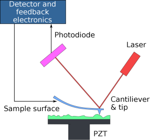
Figure 13
Applications and Uses of AFM
Currently, AFM is one of the most effective imaging techniques being used at the nanoscale and subnanoscale level. This technique has been applied to multiple problems across the field of natural sciences and can record a range of material surface properties in both liquid media and in air. Disciplines where AFM is used include:
- Semiconductor science and technology
- Thin film and coatings
- Tribology (surface and friction interactions)
- Surface chemistry
- Polymer chemistry and physics
- Cell biology
- Molecular biology
- Energy storage (batter) and energy generation (photovoltaic) materials
- Piezoelectric and ferroelectric materials
X-ray diffraction (XRD)
XRD is one of the most extensively used techniques for the characterization of nanoparticles. XRD provides information regarding the crystalline structure, nature of the phase, lattice parameters and crystalline grain size.
X-ray powder diffraction (XRD) is a rapid analytical technique primarily used for phase identification of a crystalline material and can provide information on unit cell dimensions. The analysed material is finely ground, homogenized, and average bulk composition is determined.
Powder X-ray diffraction has become a cornerstone technique for deriving crystallite size in nanoscience due to speed and "simplicity". An advantage of the XRD techniques commonly performed in samples of powder form, usually after drying their corresponding colloidal solutions, is that it results in statistically representative, volume-averaged values. The composition of the particles can be determined by comparing the position and intensity of the peaks. However, it is not suitable for amorphous materials and the XRD peaks are too broad for particles with a size below 3 nm.
Unfortunately, this apparently simple technique commonly has unexpected problems. Anisotropic peak broadening related to crystallite shape, defects, and microstrain occurs frequently in nanomaterials and can significantly complicate the analysis. In some instances, the usage of the conventional single peak approach would give erroneous results, and in others, this type of analysis is not even possible. A number of different nanocrystalline oxides have been examined to determine their crystallite sizes by different techniques. They differ in terms of crystal symmetry, crystallinity, density, and present different challenges with regard to size analysis.
Principle: X-ray diffraction is based on constructive interference of monochromatic X-rays and a crystalline sample. These X-rays are generated by a cathode ray tube, filtered to produce monochromatic radiation, collimated to concentrate, and directed toward the sample
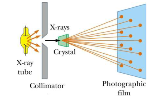
Figure 14
X-ray Diffraction (XRD) is one of the classical methods for identification and characterization of crystalline solids. Each crystalline solid has its unique characteristic X-ray powder pattern which issued as a ”fingerprint” for its identification. The method is based on the diffraction of X-rays by the sample in different directions. Waves of wavelength comparable to the crystal lattice spacing are strongly scattered (diffracted).
A powder X-ray diffractometer consists of an X-ray source (usually an X-ray tube), a sample stage, a detector and a way to vary angle θ. The X-ray is focused on the sample at some angle θ, while the detector opposite the source reads the intensity of the X-ray it receives at 2θ away from the source path. The incident angle is than increased over time while the detector angle always remains 2θ.
X-rays incident upon a crystal is scattered in different ways. When the wavelength of the radiation (λ) is comparable to the atomic spacing in a crystal, the scattering which is termed as diffraction, gives rise to a set of well-defined beams arranged with a characteristic geometry, thus forming a diffraction pattern. Schematic of X-ray diffraction setup is shown in figure.
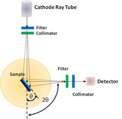
Figure 15: XRD Technique
X-ray diffraction data collection is the result of relative intensity (I) for each reflection with a set of planes in the crystal, designated by Miller indices (h k l), along with the corresponding scattering angle (2θ) for that reflection. The positions and intensities of the diffracted beams are a function of the arrangements of the atoms in space and some other atomic properties.
Thus, if the positions and the intensities of the diffracted beams are recorded, it is possible to deduce the arrangement of the atoms in the crystal and their chemical nature. A beam of radiation will only be diffracted when it imposed upon a set of planes in a crystal if the geometry of the situation fulfils quite specific law defined by Bragg’s known as Bragg’s law.
nλ =2dhklsinθ
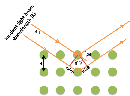
Figure 16: Bragg’s Law
The above equation is known as the Bragg equation, where n denotes the order of diffraction, λ represents the wavelength, d is the interplanar spacing of hkl planes in crystal lattice and θ signifies the Bragg angle.
A typical diffraction pattern shows the intensity Vs 2θplot. Each peak corresponds to a specific (h k l) plane of the sample. The broadening of the diffraction peaks is due to two factors:
1) Due to size of crystallite
2) Due to micro strain of crystallite
Advantages
- It is a rapid and powerful technique for identifying unknown minerals and materials
- It only requires preparation of a minimal sample for analysis
- Interpreting the resulting data is relatively straightforward
- XRD measurement instruments are widely available
Disadvantages
- To best identify an unknown powder material, the sample should be homogeneous.
- Typically XRD analysis requires access to standard reference data.
- Preparation of samples often requires grinding them down to a powder
- If the crystal sample is non-isometric, then the indexing of patterns can be complex when determining unit cells
Consider the examination results of say 10th standard in the Tamil Nadu scenario in which around 6, 00,000 number of students appear every year. In this case consider the result of the whole state as the first case, results of a district, a school and a class room as the second, third and fourth cases respectively. Let us draw the bar diagram similar to the energy level diagram for number of students having scored marks in different bands like 99-100, 98-99, 97-98 and so on.
Just visualize this bar diagram for the whole state, district, school and a class, how it will look like?
When you look at the state level mark band diagram, each band will be crowded and placed very close to each other. Here the spatial dimension of the state is larger and the number of students considered is more. This case is very similar to bulk materials where electrons are free to move in all the directions and no limitations or no confinement. In this case electronic energy level bands will be crowded as well as will be almost continuous.
When you look at the district level mark band diagram, each band will be less crowded and placed close to each other but not like state level. This is because of the reduced dimension and in-turn lesser number of students. This case is very similar to Quantum Well where electrons are free to move only in two directions and confined to one direction. In this case electronic energy level bands will not be crowded like bulk and with an increased gap between bands.
When you look at the school level mark band diagram, each band will be having still smaller number of students and bands are placed wider to each other. Here, further reduction in the dimension of the sample resulting in band widening with minimum number of students in each band. This case is very similar to Quantum Wire where electrons are free to move in only one direction and confined to two directions. In this case electronic energy level bands will be still widened and with much increased gap between bands.
Finally, when you look at the Classlevel mark band diagram, each band will be having very few numbers of students and bands are placed much wider to each other. Here a class representing the smallest dimension in terms of sample considered. This case is an analogy for the Quantum Dot. Since Quantum Dot is a nano-sized particle where electrons are totally confined and cannot move anywhere. In this case electronic energy level bands are widened to the maximum.
As we reduce the size of the materials more and more we can confine electrons more and more.

Figure 17
(a) In quantum wells, electrons are confined only in one dimension. Quantum wells are usually implemented by burying the confining material within a barrier material.
(b) Quantum wires confine electrons in two dimensions. The electron is not confined along the wire.
(c) In a quantum dot, an electron is confined in three dimensions.
Quantum Well
The term “well” refers to a semiconductor region that is grown to possess a lower energy, so that it acts as a trap for electrons and holes (electrons and holes gravitate towards their lowest possible energy positions). They are referred to as “quantum” wells because these semiconductor regions are only a few atomic layers thick; in turn, this means that their properties are governed by quantum mechanics, allowing only specific energies and band gaps. Because QW structures are very thin, they can be modified very easily.
Quantum wells are real-world implementation of the “particle in the box” problem; they act as potential wells for charge carriers and are typically experimentally realized by epitaxial growth of a sequence of ultrathin layers consisting of semiconducting materials of varying composition.
Two dissimilar semiconductors with different band gaps can be joined to form a heterojunction. The discontinuity in either the conduction or the valence band can be used to form a potential well. If a thin layer of a narrower-band gap material 'A' say, is sandwiched between two layers of a wider-band gap material 'B', then they form a double heterojunction. If layer 'A' is sufficiently thin for quantum properties to be exhibited, then such a band alignment is called a single quantum well. Additional semiconductor layers can be included in the heterostructure, for example a stepped or asymmetric quantum well can be formed by the inclusion of an alloy between materials A and B.
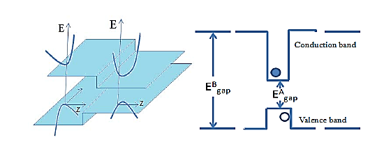
Figure 18
Still more complex structures can be formed, such as symmetric or asymmetric double quantum well and multiple quantum wells or superlattices. The difference between the them is the extent of the interaction between the quantum wells.
In particular, a multiple quantum well exhibits the properties of a collection of isolated single quantum wells, whereas in a superlattice the quantum wells do interact.
Most of the structures illustrated so far have been examples of Type-I systems. In this type, the band gap of one material is nestled entirely within that of the wider-band gap material. The consequence of this is that any electrons or holes fall into quantum wells which are within the same layer of material. Thus both types of charge carrier are localised in the same region of space, which makes for efficient (fast) recombination.
In Type-II systems the band gaps of the materials, say 'A' and 'C', are aligned such that the quantum wells formed in the conduction and valence bands are in different materials. This leads to the electrons and holes being confined in different layers of the semiconductor. The consequence of this is that the recombination times of electrons and holes are long.
Band Diagram
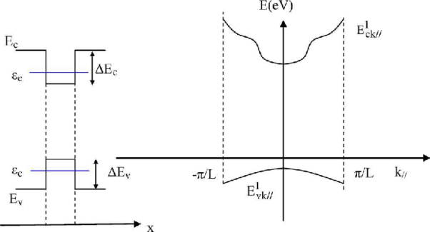
Figure 19
Quantum Wire
A quantum wire with rectangular cross-section is shown in Figure 17(b). Again, we will assume that the potential is infinite at the boundaries of the wire:
 ….(1)
….(1)
Where V0. The associated wavefunction is confined in the x-y plane and composed of plane waves in the z direction, thus we chose the trial wavefunction
 ….(2)
….(2)
Inserting Eq. (2) intothe Schrödinger equation gives (for 0 ≤ x ≤ Lxand 0 ≤ y ≤ Ly):

Since the potential goes to infinity at the edges of the wire, (x=0)( Lx =0)(y=0)( Ly =0). Thus, the solution is


Where

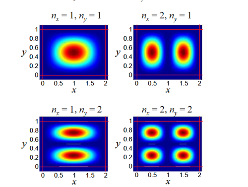
Figure 19: The first four modes of the quantum wire. Since in this example, Lx> Ly the nx = 2, ny = 1 mode has lower energy than the nx = 1, ny = 2 mode
Schematic band structure of a typical 1D quantum wire.
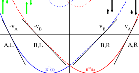
Figure 20
The red/blue curves show the s = ± bands, and the dotted curves indicate the next subband (the Fermi energy ǫF is assumed below that band). For the low-energy description, we linearize the dispersion. It is notationally convenient to introduce bands A (solid lines) and B (dashed lines). Green and black arrows indicate the respective spin amplitudes (exaggerated). The resulting Fermi momenta are ±k (A,B) F , with Fermi velocities vA,B.
We will see the variation of Energy w.r.t. Wavenumber k for a quasi-quantum wire in figure 21.
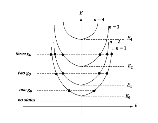
Figure 21
Quantum Dot
The 0-d DOS is a special case because the particle is confined in all directions. Like a particle in a well with discrete energy levels, we might assume that the density of states in a 0-d might be a series of delta functions at the allowed energy levels. This is indeed true for an isolated 0-d particle.The lifetime of a charge in an orbital of an isolated particle is infinite. From the uncertainty principle, infinite lifetimes are associated with perfectly discrete energy states in the isolated molecule, i.e. if  t,
t,  E 0.
E 0.
But when, for example, a molecule is brought in contact with a metal electrode, the electron may eventually escape into the metal. Now, the electron’s lifetime on the molecule is finite, and hence the molecule’s energy levels should also exhibit a finite width. Thus, molecular energy levels are broadened in a coupled metal-molecule system – the greater the coupling, the greater the broadening of the molecular energy levels.
Let’s assume that there are two electrons in the molecular orbital. Let’s assume that thelifetime of these electrons on the molecule is . Furthermore, let’s assume that the decay of the electron probability on the molecule is exponential. Then the time dependence of the electron probability in the molecular orbital is:
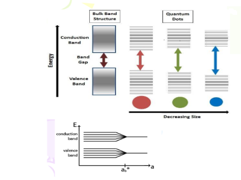
Figure 22
In the strong confinement scenario, the band gap can increase when the quantum dot is smaller than the exciton bohr radius as energy levels become split. Total emission energy is increased, as well as emission at varied wavelengths, creating white light.
The exciton Bohr radius is given by the formula:

- εr= dielectric constant (relative permittivity)
- m = mass
- μ = reduced mass
- ab = Bohr radius (0.053 nm)
Confinement Energy
The particle in a box model is also used in modeling the exciton. Variance of particle size allows for control of the confinement energy. The solution to the particle in a box model is used to represent the energy of the exciton as follows7:

Bound Exciton Energy
Coulombic attractions persist between the electron of negative charge and hole of positive charge that have an energy proportional to Rydberg's energy, and inversely proportional to the dielectric constant squared. This term becomes important when the semiconductor crystal is smaller than the exciton Bohr radius7:

A quantum dot is confined in all three spatial dimensions, but semiconductors with other modes of confinement include quantum wires (holes or electrons confined in two spatial dimensions with one degree of freedom), and quantum wells (confined in one spatial dimension with two degrees of freedom).
Taking into account each of these three terms then, the total energy can be simplified further:

Smaller crystals typically have larger electronic bandgaps, meaning that the energetic difference between energy states is greater. This results in more energy being necessary in order to move into an excited state, and more energy is increased upon returning to a rest energy. A semiconductor struck by a photon of light at higher energy that its bandgap will have an electron excited from the valence band to the conduction band (see Figure 23). This process leaves behind a hole, oppositely charged from the electron in the valence band. The hole and electron are attracted by Coulombic forces to create an exciton.
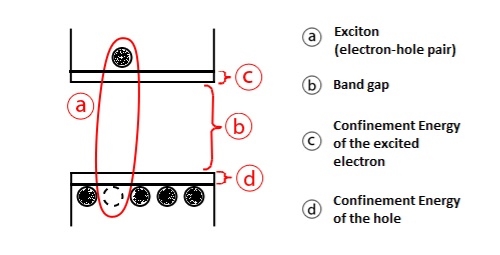
Figure 23: Creation of the exciton from the electron hole pair.