MODULE 4
MEASUREMENTS
CARRIER DENSITY, RESISTIVITY AND HALL MOBILITY
One of the most common methods of measuring a material‘s surface resistivity is using either the two-or four-point probe method .Two probe method is used to measure the resistivity of films with fairly large resistance. But if the film resistance is very small (comparable with the lead) four probe method is adopted. Measuring surface resistivity with four probes dates back to 1916 where Wenner discussed using the technique to measure the earth‘s resistivity .Both two and four probe methods are the most popular methods for measuring resistivity due to the ability of minimizing the parasitic effects of contact resistance, Rc shown below in equation (1). To illustrate why four probes are generally used, the two-point probe method is considered for comparison purposes.
In the two point probe method, two voltage probes are at a fixed spacing distance and are moved together along the material surface. Current is sent through one probe and exits through the second probe. The voltage between the two probes is measured by either a potentiometer or a voltmeter. By combining both the voltage and current measurements into the two surface probes, it is possible to calculate material surface resistance between the two probes using the calculation:
Rtotal = Voltage (V)/Current (I) = 2Rc + 2Rsp + Rs ……….(1)
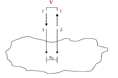
Figure 1: Two point probe test setup
Two point probe setup is shown in figure 1. The variable Rc is the parasitic contact resistance made between the material surface and the probe touching the surface. Rsp is the spreading resistance, or the parasitic resistance caused by current flowing into the sample surface. The variable of interest is Rs, or the surface resistance of the particular material. Although the two-point probe method is capable of calculating the surface resistivity, the four-point probe method is superior due to the use of two additional probes. In contrast to the two-point method, the four point method uses the two additional probes to measure the potential of the material surface. These probes do not carry any current, thus eliminating the parasitic resistances Rc and Rsp measured in the two-point probe method.
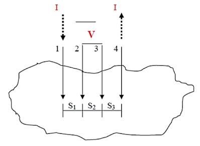
Figure 2:Four point probe test setup. Probes 1 and 4 carry current (I), 2 and 3 measure voltage (V).
In the four-point probe setup as shown in figure 2, the voltage potential V adjacent to a probe carrying current can be given by:
V = ρI/ 2πr ………….(2)
Whereρ is the surface resistivity of a material of semi-infinite size, I is the current in the probe, and r is the distance between the voltage measurement and the current probe.
A very convenient way to measure the sheet resistance of a film is to press a 4-point metal tip probe assembly in to the surface as shown in (figure 2). The outer probe is connected to current source and inner probes to detect the voltage drop.
Voltage at probe number 2 is
 …………(3)
Voltage at probe number 3 is
 …………(4)
Hence the total voltage is V
 .………..(5)
The resistivity
 .………..(6)
If all the probes are equidistant with inner probe distance S then the equation reduces to
 .………..(7)
Most surface resistivity measurements of semiconductor wafers or thin films are made on a small surface area substrate. Small spacing differences in probe spacing can cause the resistivity values to vary widely across a sample surface. A high quality four-point head is necessary to get repeatable and reliable resistivity values. When measuring samples with low resistivity, high currents are needed in the current probes to obtain good voltage readings.
VAN DER PAUW METHOD
The Van der Pauw technique can be used to measure resistivity of a thin, arbitrary-shaped, simply connected, (i.e. one without holes or non-conducting islands) sample with four Ohmic contacts placed on the periphery. The objective of the Van der Pauw technique is to measure the sheet resistance Rsof the sample. Van der Pauw demonstrated (figure 3) that there are two characteristics resistances,RAand RB, associated with the four terminals.
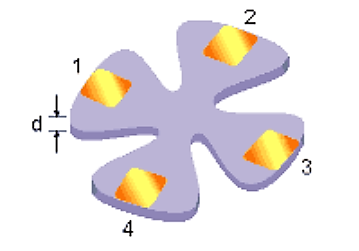
Figure 3: Illustration of Van der Pauw technique
V43 is the voltage measured across terminals 4 and 3, V14is the voltage measured across terminals 1 and 4. I12is the current measured across terminals 1 and 2. I23is the current measured across terminals 2 and 3. RA and RBrelate to the sheet resistance through the Van der Pauw equation.
 …………..(1)
Which can be solved numerically for Rs. The resistivity can then be calculated using therelation
ρ = Rsd …………..(2)
To obtain the two characteristic resistances, one applies a dc current I into contact 1 and out of contact 2 and measures the voltage V43from contact 4 to contact 3. Next, oneapplies the current I into contact 2 and out of contact 3 while measuring the voltage V14from contact 1 to contact 4. RAand RBare calculated by means of the following expressions:
RA =  …………..(3)
RB= …………..(4)
The objective in the Hall measurement in theVan-der Pauw technique is to determine the sheet carrier density nsby measuring the Hall voltage VH. The Hall voltage measurement consists of a series of voltage measurements with a constant current and a constant magnetic field B applied perpendicular to the plane of the sample. The sheet carrier density nscan be calculated via
ns= - 
To ensure the quality of the result obtained from the Hall measurement several factors must be considered. Primary concerns are Ohmic contacts quality and size, sample uniformity and accurate thickness determination and thermo-magnetic effects due to non-uniform temperature and photoconductive and photovoltaic effects which can be minimized by measuring in a dark environment. Also the lateral dimensions must be large compared to the size of the contacts and the sample thickness. Finally, one must accuratelymeasure sample temperature, magnetic field intensity, electric current and voltage.
Schematic of a Van der Pauw configuration used (figure 4) in the determination of the Hall voltage VH. To measure the Hall voltage VH, a current I is forced through the opposing pair of contacts 1 and 3 and the Hall voltage VH(= V24) is measured across theremaining pair of contacts 2 and 4. Once the Hall voltage VHis acquired, the sheet carrier densityns can be calculated via
ns = IB/q|VH| from the known values of I, B, and q.
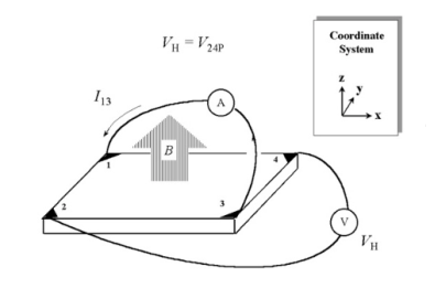
Figure 4: Hall voltage measurement
There are practical aspects which must be considered when carrying out Hall and resistivity measurements. Primary concerns are
(1) Ohmic contact quality and size,
(2) Sample uniformity and accurate thickness determination,
(3) Thermo-magnetic effects due to non-uniform temperature, and
(4) Photoconductive and photovoltaic effects
Which can be minimized by measuring in a dark environment. Also, thesample lateral dimensions must be large compared to the size of the contacts and the sample thickness.
Finally, one must accurately measure sample temperature, magnetic field intensity, electrical current, and voltage.The Hall Effect is a technique used to measure the amount and type of carriers present in a semiconductor. Due to the fact that both types of carriers (holes and electrons) increase conductivity, the carrier type cannot be determined from simple electrical measurements. The Hall Effect results from the influence of a magnetic field on moving charges (current).
The "hot-probe" experiment provides a very simple way to distinguishbetween n-type and p-type semiconductors using a soldering iron and a standard multi-meter.The experiment is performed by contacting a semiconductor wafer with a "hot" probe such as a heated soldering iron and a "cold" probe. Both probes are wired to a sensitive current meter. The hot probe is connected to the positive terminal of the meter while the cold probe is connected to the negative terminal. The experimental set-up is shown in the figure below:
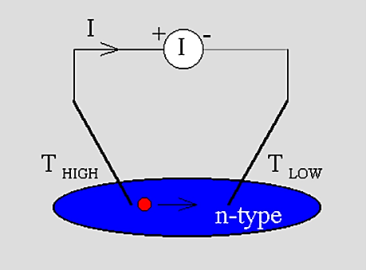
Figure 5: Experimental set-up of the "hot-probe" experiment
When applying the probes to n-type material one obtains a positive current reading on the meter, while p-type material yields a negative current.A simple explanation for this experiment is that the carriers move within the semiconductor from thehot probe to the cold probe. While diffusion seems to be a plausible mechanism to cause the carrier flow it is actually not the most important mechanism since the material is uniformlydoped. However, as will be discussed below there is a substantialelectric field in the semiconductor so that the current is dominated by the drift current.Starting from the assumption that the current meter has zero resistance, and ignoring the (small) thermoelectric effect in the metal wires one can justify that the Fermi energy does not vary throughout the material. A possible corresponding energy band diagram is shown below:
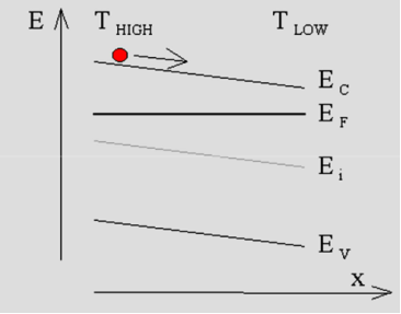
Figure 6: Energy band diagram corresponding to the "hot-probe" experiment illustrated by Figure1
This energy band diagram illustrates the specific case in which the temperature variation causes a linear change ofthe conduction band energy as measured relative to the Fermi energy, and also illustratesthe trend in the general case. As the effective density of states decreases with decreasing temperature, one finds that the conduction band energy decreases with decreasing temperature yielding an electric field which causes the electrons to flow from the high to the low temperature. The same reasoning reveals that holes in a p-type semiconductor will also flow from the higher to the lower temperature.
The current can be calculated from the general expression
 …………..(1)
Where
 …………..(2)
The current will therefore increase with doping and with the applied temperature gradient as long as the semiconductor does not become degenerate or intrinsic within the applied temperature range.
This can be understand by this example
The experiment is performed by contacting a semiconductor wafer with a "hot" probe such as a heated soldering iron and a "cold" probe. Both probes are wired to a sensitive current meter.
The hot probe is connected to the positive terminal of the meter while the cold probe is connected to the negative terminal. The experimental set-up is shown in the figure below:
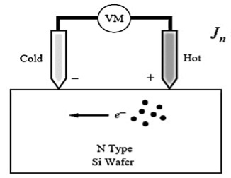
Figure 7
When applying the probes to n-type material one obtains a positive current reading on the meter, while p-type material yields a negative current.
A simple explanation for this experiment is that the carriers move within the semiconductor from the hot probe to the cold probe.
The heat source will cause charge carriers (electrons in an n-type, electron holes in a p-type) to move away from the lead.
The heat from the probe creates an increased number of higher energy carriers which then diffuse away from the contact point. This will cause a current/voltage difference.
For example, if the heat source is placed on the positive lead of a voltmeter attached to an n-type semiconductor, a positive voltage reading will result as the area around the heat source/positive lead becomes positively charged.
If the material were of p-type, positively charged holes will be majority carriers, and polarity of induced voltage would be reversed. The direction of current would also be reversed if they were shorted with a wire.
Thus a measurement of either the short circuit current or the open circuit voltage tells us the type of material.
The measurement of capacitance as a function of voltage allows for the determination of many important interface and bulk parameters, such as fixed charges, interface state densities, band offsets, carrier transport, as well as doping types and densities.
Capacitance-voltage (CV) measurements areconventionally made using a dedicated test fixture situated within a light excludingenclosure to prevent measurement errors due to extraneous photo-generated currents.
Typically, an unpatterned oxide layer is fabricated on a high quality silicon substrate, which is then metallized with a thin film of aluminium. The thin film is patterned to formMOS capacitors, either at the time of deposition by use of a shadow mask or by means of conventional photolithography and chemical etching.
Alternatively, MOS capacitors can be fabricated by depositing, heavily doping, and patterning a polysilicon thin film instead of aluminium. The advantage of the use of aluminium is that the deposition and patterning are very convenient; however, heavily doped polysilicon most closely approximates afinished transistorstructure.
Usually, electrical connection to the completed MOS capacitoris made to the topside aluminium or polysilicon contact by means of a thin tungsten probe and to the backside of the wafer by use of a conductive “chuck” which allows a partial vacuum to be drawn under the wafer, i.e., a “vacuum chuck”, thus facilitating electrical contact.
Although not absolutely necessary for capacitance measurements, it is generally advantageous to remove any pre-existing insulating layers from the back of the wafer. (Indeed, it is usual for a layer of oxide to be grown on the back as well as the front of a wafer during thermal oxidation.)
This is easily done by etching in hydrofluoric acid, hydrogen fluoride vapour, or some other method. If backside contact is found to be especially critical, the whole back of the waferoptionallymay be metallized. Furthermore, in practice,it is usual for the backside contact, i.e., the silicon substrate, to be held at ground and the frontside contact, i.e., aluminium or polysilicon, to be biased at some potential. In general, it is found that useful informationis obtained from CV measurements made fortwo different conditions,viz., quasistatic and high frequency.
Typically, this data is used to construct a “CV plot” which graphically displays MOS capacitance or capacitance per unit area as a function of bias voltage.
Quasistatic Conditions
As might be expected, quasistatic conditions correspond closely to equilibrium. Conventionally, a quasistatic CV measurement is made by sweeping bias voltage applied to an MOS capacitor so that the surface of the semiconductor changes from inversion to depletion and then to accumulation.
During this procedure, displacement current is measured as a function of time. Obviously, displacement current is just the transient charging current of the capacitor.
Ideally, there is no true conduction current flowing through the oxide layer. Even so,a small amount of “leakage current” invariably flows through any “real” oxide layer. Of course, for quasistatic measurements to be useful the oxide must not be too “leaky”, otherwise, conduction current will be added to displacement current and measurements will be inaccurate.
Generally, for a high quality oxide this current is negligible and can be ignored. The integration of charging current over time merely results in a measurement of the charge stored in the MOS capacitor; hence,capacitance as a function of voltage is determined by elementary identification of the product of capacitance and voltage as stored charge, i.e., CVQ.
Clearly, if the surface of the semiconductor is either in accumulation or inversion, a layer of charged mobile carriers is present directly beneath the oxide.
Note: For notational convenience, an italicized C denotes capacitance per unit area and a non-italicized C denotes absolute capacitance.
Thus, the measured capacitance, Cmax,is just the capacitance of the oxide layer alone which is equal to Cox A
Where A is the area of the gate, i.e., the front side contact.
In contrast, if the semiconductor is depleted, there is no layer of mobile carriers present underneath the oxide, i.e., at the Si/SiO2interface. However, mobile carriers are present underneath the depletion region. Therefore, in depletion, the measured capacitance consists of the series combination of the oxide capacitance and the capacitance of the depletion layer. Of course, this combined capacitance must be less than Cmax. Accordingly, as the voltage is swept from inversion to accumulation, during depletion the capacitance decreases from Cmaxto a minimum, Cmin, corresponding to maximum depletion layer width and then risesagain asthe semiconductor becomes accumulated. This essential behaviour illustrated in the following figure:
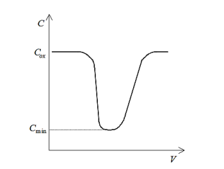
Figure 8: Idealized quasistatic CV plot
Clearly, Cminis related to Coxand Csas follows:
 =
= 
As defined previously,  and
and  are, respectively, thickness and dielectric constant of SiO2. Likewise,
 and
and  are maximum thickness and dielectric constant of the depletion layer. Of course, electrical chargesare stillpresent within the depletion region due to ionized impurity atoms; however, these charges are fixed and do not move in response to an applied bias (at low temperatures). Consequently, these fixed chargescan make no contribution to displacement current and do not result in a contribution to measured capacitance.
High Frequency Conditions
In quasistatic measurements, capacitance is measured directly by integrating charging current. However, CV measurements can also be made by superimposing a small sinusoidally oscillating (AC) signal on the voltage sweep and measuring the corresponding impedance directly as a function of bias voltage.
In this case, capacitance measured under conditions of accumulation and depletion can be expectedto bethe same as observedin quasistatic measurements, i.e., conditions still remain near equilibrium. However, if the frequency of the AC signal is sufficiently high, capacitance measured under a condition ofinversion is not the sameas in the quasistatic case. The explanation for this is quite simple and is a direct consequence of non-equilibrium behaviour of the inversion layer. Physically, any inversion layer must be formed from minority carriers generated in the depletion region and swept to the surface by the electric field.
Equilibrium conditionsimply thatthere is sufficient time for the inversion layer carrier concentrationto respond to any changes in applied field. However, if the material quality of the silicon is good, carrier generation-recombination processes occur very slowly, with a time constant on the order of milliseconds. Therefore, for an applied AC voltage inthe megahertz range, the response of the inversion layer is simply too slow to “follow” the signal and similar toionized dopant impurity atoms, the inversion layer appears fixed with respect to the AC component of the bias. This behaviour is shown in the following figure:
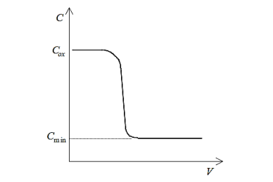
Figure 9: Idealized high frequency CV plot
Therefore, forhigh frequency conditions, the capacitance per unit area measured in inversion is the series combination of oxide capacitance per unit area and capacitance per unit area of the depletion region. Furthermore, since, the depletion width reaches a maximum value,the combined capacitance per unit area saturates at Cmin.
Interpretation of Ideal Capacitance-VoltageMeasurements
In principle, measurements of capacitance versus voltage can be made either by sweeping the applied voltage from accumulation to inversion (to + voltage for p-type; + to for n-type) or inversion to accumulation (+ to voltage for p-type; to + for n-type).
For quasistatic measurements the direction of the sweep makes essentially no difference in the form of the CV plot, again, since the MOS capacitor remains nearly at equilibrium. However, for high frequency measurements, the form of the CV plot can differ in the inversion region depending on the direction and rate of the voltage sweep. As asserted previously, this behaviour is due to the kinetics of minority carrier generation. Clearly, if the time constant for generation-recombination processes is long (indicative of a high quality substrate), then the inversion layer maynot fully form during a fast voltage sweep from accumulation to inversion. Thus, the depletion region maygrow larger than one would otherwise expect for equilibrium conditions. This phenomenonis called deep depletionand is illustrated below:
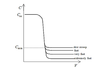
Figure 10: Deep depletion for sweep from accumulation to inversion
A new method for extracting junction parameters of the single diode model is presented. At least squares method approach considers the deviation V=f(I) between the experimental current-voltage(I-V) characteristic and a theoretical arbitrary characteristic. Specific case- the
  V graph reducing to a straight line-is identified and the knowledge of the slope and of the intercept with the ordinate axis leads to the determination of the junction parameters. The method is applied to the characterization of the emitter-base junction of transits or sand the results are discussed.
The p-n junction current voltage (1-V) characteristics have been studied for the past twenty years by many authors. Mathematical models based on the principles of solid-state physics are reasonably well developed. From the one exponential model, the (I-V) characteristic can be described by the equation:
 ………….(1)
Where kT/qisthethermalvoltage,
I0 is the saturation current,
A is the junction ideality factor,
Rs and Rsh are respectively these series and shunt resistances.
Equation (1) introduces four parameters I0,A,Rs,Rsh, related to internal properties of the electronic device.
Recent studies provided discussions to relate these parameters to the space charge re combination processes in p-n junctions. The effect of bulk and surface recombination on the value of the ideality factor of gate controlled diodes has been analysed. The variation of the junction parameters, with the illumination level, for a solar cell has been studied and associated with the modification of the carrier transport process when illumination increases. The degradation of the junction parameters of transistor devices due to ionizing radiations has been shown to be controlled by the total dose and related to radiation-induced damage. A study of the evolution of the junction parameters of sub micronic n-MOS transistors following electrical ageing has led to an evaluation of the magnitude of hot carrier degradation and this evolution has been found to be dependent on the device dimensions.
Several methods have been proposed to measure the parameters I0,A,Rs,Rsh by using the description of the experimental junction characteristic obtained with Eq.(1). They were developed for solar cells. Some were based on the consideration of I-V measurements obtained for dark and illumination conditions or on parameter approximations with numerical process involving determinations around particular points.
Others were based on curve fitting methods which consider three regions of the characteristic: short circuit current, open circuit voltage and around the maximum power point. All methods require every low level current measurements near the origin used for determination off in it shunt resistance value. Whenever the shunt resistance values are very high, a high quality and sensitive measurement system is necessary to avoid uncertainties in the determination of the parameters.
The aim is to present a new method to extract the junction parameters from the (I-V) characteristic whenever the shunt. Resistance value is very high. This simple and fast extraction technique involves the high voltage part of the characteristic and can easily be implanted in technological processes for quality control. A simulation is performed to compare the results with theoretical values of the parameters. The method is applied to characterize the base-emitter junction of transistors.
METHOD
In silicon components, diodes, bipolar transistors and MOSFETs, the junctions are of good quality. For these junctions, the shunt resistance Rsh is very high and the expression (V-RsI)/Rsh is small by comparison with the other terms in Eq.(1).Moreover, the calculations are performed here for voltage values greater than 0.4 V and the term is completely negligible with respect to the exponential term. Taking into account these remarks, relationship (1) is reduced to:
 ………….(2)
For this method, a similar equation is considered for another characteristic:
 ………….(3)
Where the values of the parameters R’s, A’ and I’0 are arbitrary. Combining Equations (2) and (3), the difference ∆V = V’-V may be written in the form:
 ………….(4)
When A = A’, the curve: ∆V= f(I)becomes a straight line:
 ………….(5)
From these results, a numerical process may be elaborated to extract the parameters Rs, A and I0 of a junction from its experimental V = f (I)characteristic.
A theoretical characteristic V’=f(I) Equation (3) is considered with arbitrary values R’s ,A ’and I0. Then, A’ is varied to determine the value A’ = A so that ∆V becomes a linear function of the current. It is performed, while varying A’, by seeking the maximum value of the linear correlation coefficient R2(Figure 11) between the experimental and the theoretical characteristics.
The slope a and the origin ordinate value b of the obtained straight line in Equation (5)yield:
 ………….(6)
And
 ………….(7)
This procedure leads to obtain, with Equation(2) a fairly exact fit to the experimental(I,V)characteristic. Figure 12 illustrates this result and shows both an experimental junction (I,V) characteristic (dotted line) and the graph of function V given by Equation (2)for parameters I0,Rs,and A values extracted by the above procedure.
∆V (V)
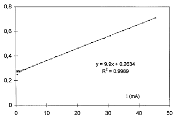
Figure 11: Difference ∆V between an experimental (dotted line) and an arbitrary characteristic versus current I for maximum values of the correlation coefficient (A= A’=1.89).
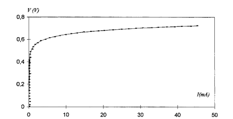
Figure 12: Description of the experimental (IV) characteristic (dotted line)with the one exponential model
This method is appropriate for the characterization of good quality electronic devices (diodes, transistors, solar cells,) with a large shunt resistance. It is of practical interest since the fitting of I-V characteristics needs the determination of only one parameter by using a least squares method. The fastness of the procedure makes it easy to implement in industrial process for quality control.
Deep Level Transient Spectroscopy (DLTS) is an efficient and powerful method used for observing and characterizing deep level impurities in semiconductors. The method was initially introduced by D. V. Lang in 1974. DLTS is a capacitance transient thermal scanning technique, operating in the high frequency (Megahertz) range. It uses the capacitance of a p-n junction or Schottky barrier as a probe to monitor the changes in charge state of a deep centre.
The capacitance techniques used before DLTS lacked either in sensitivity, speed, range of observable trap depths, or the spectroscopic nature, thus rendering the techniques inadequate for a complete characterization of a deep level.
DLTS has the advantage over all the techniques used to-date in that it fulfils almost all the requirements for a quick and complete characterization of a deep centre.
DLTS is a technique, which is sensitive enough, rapid and easy to analyze.It is able to distinguish between majority- and minority-carrier traps. DLTS can also give the concentrations, energy and capture rates of both kinds of traps.
It is spectroscopic in the sense that it can also resolve signals due to different traps. In the many variants of the basic DLTS technique the deep levels are filled with free carriers by electrical or optical methods.
Subsequent thermal emission processes give rise to a capacitance transient. The transient is analyzed by signal processing while the temperature is varied at a constant rate. This results in a full spectroscopic analysis of the semiconductor band-gap.
For a complete understanding of DLTS we must have some basic knowledge of capacitance transients arising from the depletion region of a p-n junction. The use of capacitance transients for studying the properties of defect centers is well known. These transients provide information about an impurity level in the depletion region by observation of the capacitance transient originating from the return to thermal equilibrium after a perturbation is applied to the system.
The capacitance transients is given by
C(t)=C0[1 exp(
exp( )]
)]
The capacitance transientscan be obtained by holding the sample at constant bias and temperature and applying a single filling pulse. The resultant isothermal transient can then be analyzed to obtain the emission rate of the carriers at that particular temperature. For obtaining a wide range of emission rates, this is a time consuming technique. Also if a lot of deep levels are present, the experiment and its analysis become difficult. This is where DLTS has a major edge over the conventional techniques.
The essential feature of DLTS is its ability to set up a rate window so that the measuring apparatus gives an output only when a transient occurs with a rate within the window. This concept is illustrated in Figure 2. Thus if the sample temperature is varied at a constant rate, causing the emission rate of carriers from defect center(s) present in it to vary, the measuring instrument will give a response peak whenever the defect center emission rate is within the window.
Instead of talking about rate window, we can say that the DLTS technique uses a time filter, which gives an output signal only when the transient has a time constant coinciding with the center of the time window of the filter.
A very important property of such a filter (time or rate) is that the output is proportional to the amplitude of the transient. Thus we can excite the diode repeatedly while the temperature is varied and by scanning over a large temperature interval we can directly get information as to which levels are present, what are their concentrations and by using different time/rate windows we can obtain the thermal activation energies of the levels.
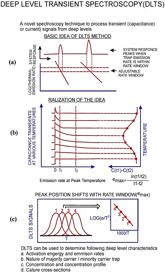
Figure:13
There are many ways of constructing a time filter. One of the widely used methods is one in which a variation of the dual-gate boxcar integrator is employed. It precisely determines the emission rate window and provides signal-averaging capabilities to enhance the signal-to-noise ratio, making it possible to defect center having very low concentrations. The use of a double boxcar for rate window selection is illustrated in Figure 13 b. The capacitance transients are observed on a fast-response capacitance bridge.
A series of transients for a typical defect center are shown on the left-hand side of Figure 13 b. These transients are fed into the double boxcar with gates set at t1 and t2. The boxcar measures the capacitance at the two times t1 and t2. The difference C(t1) - C(t2) = ∆C is calculated. It is clear from the figure that this ∆C goes through a maximum. This ∆C after going through some filtering is converted into the DLTS output S(T) given by (assuming an exponential transient):
S(T)=ΔC0[exp(−t1/τ)−exp(−t2/τ)]
Where ∆Co is the capacitance change due to the pulse at time t = 0.
It can easily be seen that S(T) really has a maximum for a certain time constant τmax.
First consider a transient that is very rapid. Then it has already finished before the first gate opens and hence C(t1) = C(t2), and S(T) =0. Similarly when the transient is too slow, it will not change much between the two gates and so again S(T) =0. Thus there will be an output with some maximum value Smax only for transients having time constants in between these two.
We can get τmax by differentiating S with respect to t and setting the derivative equal to zero. This gives:
τmax=(t1−t2/ln(t1/t2)=(x−1)t1/ln(x)
Where
x=t2/t1
Substituting this value in the expression for S gives Smax as:
Smax=ΔC0[exp(−ln(x)/(x−1))−exp(−xln(x)/(x−1)]
Thus it is seen that the peak height is independent of the absolute value of t1 and t2, rather it depends upon their ratio. Moreover, it is seen that Smax is proportional to ∆Co and therefore to the defect centre concentration NT. Therefore, the DLTS peak height can directly give the defect centre concentration.
Ultraviolet -Visible Spectroscopy is one of the oldest and most widely used method in molecular spectroscopy. Within the whole electromagnetic spectrum, only ultraviolet and visible range which occupies only a very narrow frequencyregion corresponds to the discrete atomic or molecular energy levels. So called ‘electronic spectroscopy. Excitation of electrons in both atoms and molecules are due to the absorption of light in the ultraviolet and visible range. Since the energy levels of matter are quantized, excitation will only happen if the energy of incident light is exactly the energy required of the excitation. Larger energy gap between the energy levels requires wavelengths of higher energy, resulting in absorption of shorter wavelength light. On every possible excitation, electrons are excited from a low energy ground state which is a completely filled orbital to a higher energy excited state empty anti-binding orbital.
UV-visible spectroscopy of wavelength is shorter than visible light, but longer than X-rays. UV-Violet colour is the shortest wavelength in the visible spectrum. The typical range of UV-wavelength is 10-300nm.UV is invisible to human eyes.
UV-absorption can be analyzed when a beam of light is passing through the sample and it is reflected from the surface of the sample. UV-absorption forms at a single or a wide range of spectral wavelengths. During the transition of electrons the excitation takes place to higher energy levels. UV-Visible is used to identify inorganic complexation of molecules and their qualitative and quantitative measurements .The main role for UV-Visible is to identify the properties of optical and electronic materials and to characterize the absorption, transmission, and reflectivity materials.The working principal of UV-Visible spectra is as shown in Figure 14
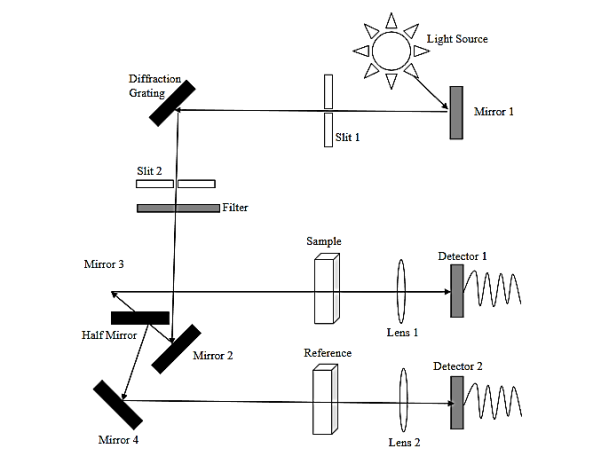
Figure 14: The working principal of UV-Visible spectra
The basic working principle of UV/Vis spectroscopy is the excitation of electrons across energy levels that correspond to radiation in the ultraviolet or visible region of electromagnetic spectrum. The internal energy of any molecule can be considered as a sum of the energy of electrons, energy associated with the vibration of constituent atoms andthe energy of rotation of molecule. Rotational levels are so close that the microwave and far infrared radiations can bring about rotational changes.The transitions across vibrational levels are possible by the absorption of infrared radiation. However, the electronic energy levels of molecules are wellseparated and only the absorption of high energy photon having energy in the ultraviolet level or visible region of the electromagnetic spectrumcan excite a molecule to a higher level.
Generally, there are three types of electronic orbitals in which valence electrons can be found. They are σ bonding orbitals (single bond), π bonding orbitals (double or triple bonds) and non-bonding orbitals (lone pair electrons).
Non-bonding orbitals have the maximum energy followed by π bonding orbitals and σ bonding orbitals. When a photon of sufficient energy is absorbed, a transition occurs from one of these orbitals to an empty antibonding orbital (σ* or π*orbital) as shown in figure 15. The energy difference between the orbitals is determined by the types of atoms and the nature of bonding. The most energetic transitions that include the absorption of a high energy photon involves only π->π*, n->π* and n->σ* transitions. However,the d->d transition of d-block element complexes is an exception.
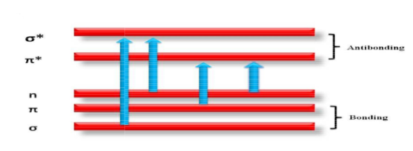
Figure15 : electron transmission in UV-Visible spectroscopy
There are mainly two types of measurement techniques in UV/Vis spectroscopy. These are absorbance and reflectance measurements
a) Absorption spectroscopy:
UV/Vis absorption spectroscopyis a frequently used technique to determine the band gap energy of semiconductor nanoparticles and thin films.The main processes involvedin this methodare absorption and transmission of light by the materials under study. Normally,the conditions under which the sample is examined areadjustedin such a way thatthe reflection,scattering and fluorescence are kept to a minimum. For examining the powder samples, usually they are dispersed in liquid media like water, ethanol or methanol before transferring it to a cell. Then amonochromatic radiationis passedthrough this solution, during which it emits radiation, the intensity of which is related tothe thickness (t) and concentration (C) of solution.
The ratio of the intensity of incident light to transmitted light is a measure of absorption.
According to Beer-Lambert law, the relation between absorbance and concentration of an absorbing species is given by
A=log(I0/I)=kcL ………….(1)
Where I0is the intensity of the incident light, I is the intensity of transmitted light, k is the molar absorptivity, c is the concentration and L is the path length.
This is measured and recorded by the instrument. The UV/Vis spectrum of most molecules consists of some humps instead of sharp spectral lines which clearly suggestthat a band of wavelengths is absorbed. This is because even a photon with too little energy to be accepted for electronic transition is used to produce vibrational and rotational transitions. An analysis of this absorption band can give vital information about the electronic structure of the material.
b) Diffused reflectance spectroscopy:
Band gap determinationUV/Vis absorption spectroscopy is a wonderful tool for determining the bandgap energy of thin films due to the low scattering from it. However, the technique can’t be used to characterize colloidal samples due to theirenhanced scattering effects. Even samples dispersed in solutions like water, methanol etc., cannot be properly characterized with absorption spectroscopy if the size of the particle is not sufficiently small to stop precipitation. In order to avoid these complications, diffused reflectance spectroscopy (DRS) can be employed. This technique is based on the focused projection of the light beam into the sample where it is reflected, scattered and transmitted through the sample material. The light reflecting off the surface is typically lost. Only the beam that passes through a particle can either reflect off the next particle or be transmitted through the next particle.
This transmission-reflection event can occur many times in the sample, which increases the path length and the scattered beam is eventually collected by the detector to gather information. From the reflectance data, absorption coefficient can be calculated. The parabolic approximation of the bandstructure predicts the relationship between absorption coefficient and bandgap energy of direct bandgap semiconductors as
(αhν)2=c2(hν-Eg) ………..(2)
Where Egis the band gap energy, α is the linear absorption coefficient of the material, hν is the photon energy and c is the proportionality constant.
To determine the bandgap energy using the above equation, a plot between (αhν)2and hν will be made. This is the well-knownTaucplot. The plot will have a linear region indicating the onset of absorption. An extrapolation of this linear region to (αhν)2=0, gives the bandgap energy of the material. Since this is a widely used method for determining the bandgap energy (Eg) of semiconductor nanostructures, it is adopted to characterize the samples in the present study.
In a semiconductor material the charge carriers is generated by optical photons. The absorption takes in any material due to the fallowing aspects
i).Charge carriers electrons
Ii).Valence band electrons
Iii).Excitation of electrons
Iv).Inner shell electrons
The valance band in a semiconductor is fills with electrons, such that the excitation takes place to higher energy levels during the absorption process. As the photon energy in a semi conducting materials the quantization of energy tends to transfer of electrons from valence band to conduction band. Direct band gap and indirect band gap of optical transitions tales place in a semi conducting materials. This two type band gap involves in the interaction withan electron in the valence band. However, direct band gap involves a vertical transition of electrons from the valence band to the conductionband. Whereasindirect band gap involves simultaneous interaction with lattice vibrations. Direct band gap transition the moment of electrons have stabilized hence energy is conserved, and the moment of electrons takes place by phonons in indirect band gap.
Absorption coefficient (α) was calculated by using the following equations
I=Ioexp (-αx) ……………(1)
Hence α=2.303/x,
Log (I/Io) = (2.303/x)A
In the energy level the photon is incident by its energy direct band gap obtained and the absorption coefficient is given by
αhυ= C (hυ-Eg)1/2
WhereC is Constant which is dependent on the structure of sample,α is the absorption coefficient and h is a planks constant.
In an energy level phonon is required for transitions, where the absorption coefficient is fallowing by
αhυ= A (hυ-Eg -Ep)2+B (hυ-Eg -Ep)2 ……………(2)
The optical absorption takes place in semiconductorsand depends on the important points which are given below.
i).The electronic transitions of elements are constant
i).The absorption and emission process are under consideration.
UV-visible Spectroscopyis used for identify the energy band gap values of the materials in the transmitting radiation. In an energy level aphoton is absorbed in its orbit. When an electron is jumps from lower energy level to higher energy level. Transitions takes place in a band gap energy as it rise in the absorption process called as absorption edge, where the optical band gap energies be determined.
Conducting materials are having energy bands and classified in to two types (1) Direct band gap (2) Indirect band gap. The top of the valence band and bottom of the conduction band are same i.e. zero crystal momentum then direct band gap takes place, where as in indirect band gap The top of the valence band and bottom of the conduction band are invariant i.e. zero crystal momentum, which is accumulated with phonon of magnitude of crystal momentum. The schematicdiagram of Optical direct and indirect band gap is shown in Figure 16
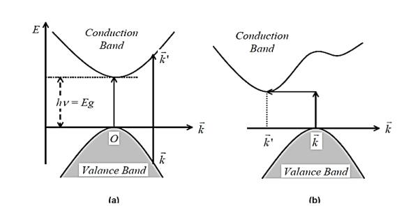
Figure 16: “Direct inter band optical transitions” for a) Direct band b) Indirect band semiconductors.