Unit 2
Transistor Characteristics
Transistor Characteristics plots the relationships between current and the voltages of transistor in a particular configuration. By considering the transistor configuration circuits to be analogous to two-port networks, they can be analysed using the characteristic-curves which are of the following types:
A transistor is an electronic device that can be used as an amplifier or electronic switch. It can amplify the signal or switch high power loads using a small signal which makes it useful in the field of electronics.
BJT has three terminals Collector (C), Emitter (E) and Base (B). It has a vertically oriented four-layers structure. The vertical structure is used to increase the cross-sectional area.
There are two types of BJT
n-p-n transistor
p-n-p transistor.
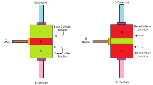
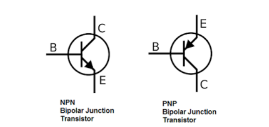
NPN transistor PNP transistor
Figure NPN and PNP transistor
It has four layers. The first layer is a heavily doped emitter layer (n+). The second layer is moderately doped the base layer (p). The third region is lightly doped collector drift region (n-). The last layer is a highly doped collector region (n+).
The drift layer (n-) increase the voltage blocking capacity of the transistor due to the low doping level. The width of this layer decides the breakdown voltage.
The power handling capacity of this transistor is too large. So, theydissipate power in the form of heat. Sometimes, heat sink is used to increase effective area and therefore increase power dissipation capacity.
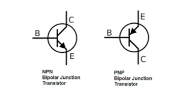
Figure . Symbol for NPN and PNP transistor
Operation:
BJT has two junctions base-emitter junction and base- collector junction. There are four different regions of operation in which either of the two junctions are forward biased reverse biased or both.
The BJT can be effectively operated in different modes according to the external bias voltage applied at each junction that is active region, saturation, and cut-off.
The other region of operation of BJT is called as inverse active region.

The figure shows an n-p-n transistor biased in the active region. The BE junction is forward biased whereas the CB junction is reversed biased. The width of the depletion region of the BE junction is small as compared to that of the CB junction.
The forward bias at the BE junction reduces the barrier potential and causes the electrons to flow from the emitter to the base. As the base is thin and lightly doped it consists of very few holes so some of the electrons from the emitter (about 2%) recombine with the holes present in the base region and flow out of the base terminal.
This constitutes the base current which flows due to recombination of electrons and holes the remaining large number of electrons will cross the reverse-biased collector junction to constitute the collector current.
Therefore,
IE = IB + IC
The base current is very small as compared to emitter and collector current.
Therefore IE ˜ IC
Heremajority of charge carriers are electrons. The operation of a p-n-p transistor is same as of the n-p-n, the only difference is that the majority charge carriers are holes instead of electrons. Only a small part current flows due to majority carriers and most of the current flows due to minority charge carriers in a BJT. Hence, they are called as minority carrier devices.
Amplification:
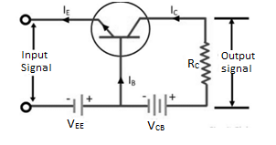
Transistor raises the strength of a weak signal and hence acts an amplifier. The transistor amplifier circuit is shown in the figure below.
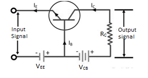
The transistor has three terminals namely emitter, base and collector. The emitter and base of the transistor are connected in forward biased and the collector base region is in reverse bias. The forward bias means the P-region of the transistor is connected to the positive terminal of the supply and the negative region is connected to the N-terminal and in reverse bias just opposite of it has occurred.
Vee is applied to the input circuit along with the input signal to achieve the amplification. The DC voltage VEE keeps the emitter-base junction under the forward biased condition regardless of the polarity of the input signal and is known as bias voltage.
When a weak signal is applied to the input, a small change in signal voltage causes a change in emitter current this change is almost the same in collector current because of the transmitter action.
In the collector circuit, a load resistor RC of high value is connected. When collector current flows through such a high resistance, it produces a large voltage drop across it. Thus, a weak signal (0.1V) applied to the input circuit appears in the amplified form (10V) in the collector circuit.
The three types of configurations are Common Base, Common Emitter and Common Collector configurations. In every configuration, the emitter junction is forward biased and the collector junction is reverse biased.
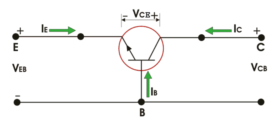
Common Base Configuration
The Base terminal is taken as common terminal for both input and output of the transistor. The common base connection for both NPN and PNP transistors is as shown in the figure.
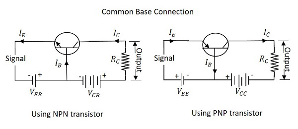
Let us consider NPN transistor in CB configuration. When the emitter voltage is applied, as it is forward biased, the electrons from the negative terminal repel the emitter electrons and current flows through the emitter and base to the collector to contribute collector current. The collector voltage VCB is kept constant throughout this.
In the CB configuration, the input current is the emitter current IE and the output current is the collector current IC.
Current Amplification Factor α
The ratio of change in collector current $ΔIC$ to the change in emitter current $ΔIE$ when collector voltage VCB is kept constant, is called as Current amplification factor. It is denoted by α.
α=ΔIC/ΔIEatconstantVCB
Expression for Collector current
Along with the emitter current flowing, there is some amount of base current IB which flows through the base terminal due to electron hole recombination. As collector-base junction is reverse biased, there is another current which is flown due to minority charge carriers. This is the leakage current Ileakage. This is due to minority charge carriers and hence too small.
The emitter current that reaches the collector terminal is
αIE
Total collector current
IC=αIE+Ileakage
If the emitter-base voltage VEB = 0, there flows a small leakage current, which can be termed as ICBO collector−basecurrentwithoutputopencollector−basecurrentwithoutputopen.
The collector current therefore can be expressed as
IC=αIE+ICBO
IE=IC+IB
IC=α(IC+IB)+ICBO
IC(1−α)=αIB+ICBO
IC=α/1−αIB+1/1-α ICBO
If the base current IB=0
The collector emitter current with base open is ICEO
ICEO=1/1−αICBO
Substituting the value of this in the previous equation, we get
IC=α/1−αIB+ICEO
IC=βIB+ICEO
Hence the equation for collector current is obtained
Characteristics of CB configuration
η=ΔVEB/ ΔIEatconstantVCB
ro=ΔVCB/ΔICatconstantlE
Common Emitter CE Configuration
The Emitter terminal is taken as common terminal for both input and output of the transistor. The common emitter connection for both NPN and PNP transistors is as shown in the following figure.
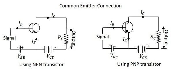
The emitter junction is forward biased and the collector junction is reverse biased. The flow of electrons is controlled in the same manner. The input current is the base current IB and the output current is the collector current IC here.
Base Current Amplification factor β
The ratio of change in collector current $ΔIC$to the change in base current $ΔIB$ is known as Base Current Amplification Factor.
It is denoted by β
β=ΔIC/ΔIB
Relation between β and α
To derive the relation between base current amplification factor and emitter current amplification factor.
β=ΔIC/ΔIB
α=ΔIC/ΔIE
IE=IB+IC
ΔIE=ΔIB+ΔIC
ΔIB=ΔIE−ΔIC
We can write
β=ΔIC/ΔIE−ΔIC
Dividing by ΔIE
β=ΔIC/ΔIE/ΔIE/ΔIE−ΔIC/ΔIE
We have
α=ΔIC/ΔIE
Therefore,
β=α/1−α
From the above equation, it is evident that, as α approaches 1, β reaches infinity.
Hence, the current gain in Common Emitter connection is too high. This is the reason this circuit connection is mostly used in all transistor applications.
Expression for Collector Current
In the Common Emitter configuration, IB is the input current and IC is the output current.
We know
IE=IB+IC
And
IC=αIE+ICBO
=α(IB+IC)+ICBO
IC(1−α)=αIB+ICBO
IC=α/1−αIB+1/1−αICBO
If base circuit is open, i.e. if IB = 0,
The collector emitter current with base open is ICEO
ICEO=1/1−αICBO
Substituting the value of this in the previous equation, we get
IC=α/1−αIB+ICEO
IC=βIB+ICEO
Hence the equation for collector current is obtained.
Characteristics of CE Configuration
ri=ΔVBE/ΔIBatconstantVCE
ro=ΔVCE/ΔICatconstantIB
Common Collector CCConfiguration
The Collector terminal is taken as common terminal for both input and output of the transistor. The common collector connection for both NPN and PNP transistors is as shown in the following figure.
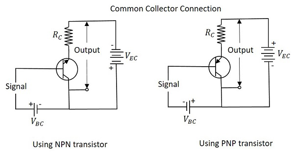
Current Amplification Factor γγ
The ratio of change in emitter current $ΔIE$$ΔIE$ to the change in base current $ΔIB$ is known as Current Amplification factor in common collector CC configuration. It is denoted by γ.
γ=ΔIE/ΔIB
Relation between γ and α
Let us try to draw some relation between γ and α
γ=ΔIE/ΔIB
α=ΔIC/ΔIE
IE=IB+IC
ΔIE=ΔIB+ΔIC
ΔIB=ΔIE−ΔIC
Substituting the value of IB, we get
γ=ΔIE/ΔIE−ΔIC
Dividing by ΔIE
γ=ΔIE//ΔIE/ΔIE/ΔIE−ΔIC/ΔIE
γ=1/1−α
Expression for collector current
We know
IC=αIE+ICBO
IE=IB+IC=IB+(αIE+ICBO)
IE(1−α)=IB+ICBO
IE=IB/1−α+ICBO/1−α
IC≅IE=(β+1)IB+(β+1)ICBO
The above is the expression for collector current.
Characteristics of CC Configuration
Approximate analysis
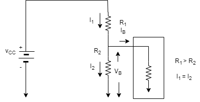
Transistor Analysis

Load Line Analysis
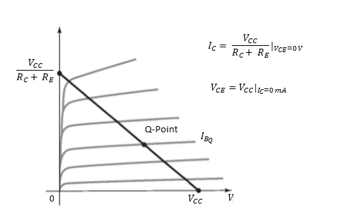
Determine the levels of ICQ and VCEQ for voltage divider configuration using exact and approximate techniques and compare solutions.
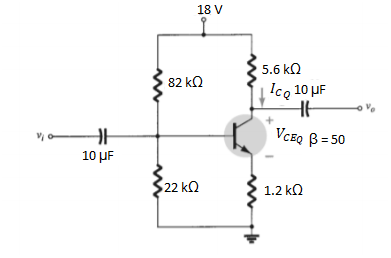
β . RE ≥ 10 R2
(50)(1.2 k Ω) ≥ 10(22 k Ω)
 60kΩ≥ 220kΩ
Rth = R1 || R2 82 kΩ || 22 kΩ = 17.35 kΩ
Eth = R2 Vcc/ R1 + R2 = 22kΩ (18V)/ 82kΩ + 22kΩ = 3.81 V
IB = Eth – VBE/ Rth + (β +1) RE = 3.81 V – 0.7V / 17.35 kΩ + (51 )(1.2kΩ) = 3.11/ 78.55 kΩ = 39.6 μ A
ICQ = β IB = (50)(39.6μA) = 1.98 mA
VCEQ = Vcc – IC(RC + RE)
= 18V – (1.98mA)(5.6kΩ + 1.2 kΩ)= 4.54V
A field-effect transistor or FET is a transistor, where the output current is controlled by an electric field. FET sometimes is called unipolar transistor as it involves single carrier type operation.
FET is three-terminal semiconductor devices, with source, drain, and gate terminals.
The charge carries are electrons or holes, which flow from the source to drain through an active channel. This flow of electrons from source to drain is controlled by the voltage applied across the gate and source terminals.
The terminal connected to one end of the n channel is called drain terminal and the terminal connected to the other end of the channel is called the source terminal. The metallic terminal connected to the layer surrounding the channel of opposite type semiconductor material (here it is p-type) is known as the gate terminal.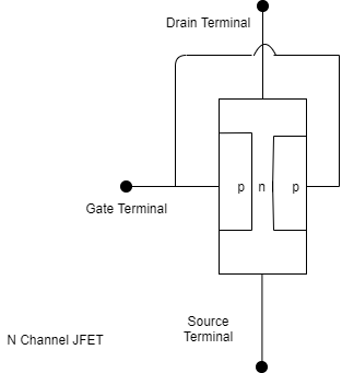
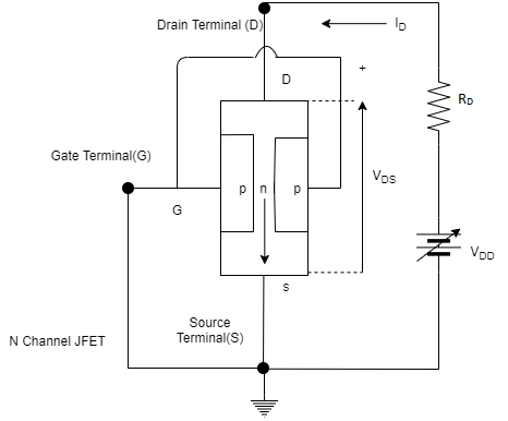
If we connect the external circuit with these three terminals. The positive terminal of a voltage source circuit at the drain of the transistor. The negative end of the voltage source would be grounded. The gate terminal is also connected to the ground as shown.
At this condition n channel gets higher potential than gate region hence junction between the p-type gate region and n-type channel region would be in reverse biased condition.
As a result, the depletion layer of this junction becomes thicker, and apparently, the thickness of the depletion layer depends on the voltage difference between these two regions.
Considering the potential of the channel near the drain is more than the source terminal. This is because the positive terminal of the voltage source gets connected at the drain and source terminal is grounded.
The voltage distribution along the channel that is the portion of the junction near the drain gets more voltage than the lower portion of the junction. Because of this the width of the depletion region near the drain is more.
At this condition there is a flow of majority carriers in the n-channel due to applied electric field between drain and source.
If we increase the drain voltage slowly then the current through FET channel increases slowly. But this linearity does not continue after a particular drain voltage. This voltage is called pinch-off voltage.
At the pinch-off voltage, the depletion layers touch each other and theoretically blocks the channel. So, drain current that is current through the channel becomes zero but practically the current will not be zero but rather a constant value.As a result, the resistance of the channel increases proportionately which keeps the drain current almost constant.
The depletion type MOSFET transistor is equivalent to a “normally closed” switch. The depletion type of transistors requires gate – source voltage (VGS) to switch OFF the device.
Symbols of Depletion Mode MOSFET
The symbols for depletion mode of MOSFETs in both N-channel and P-channel types are shown above. The fourth terminal substrate is connected to the ground, but in discrete MOSFETs it is connected to source terminal. The continuous thick line connected between the drain and source terminal represents the depletion type. The arrow symbol indicates the type of channel, such as N-channel or P-channel.
In this type of MOSFETs a thin layer of silicon is deposited below the gate terminal. The depletion mode MOSFET transistors are generally ON at zero gate-source voltage (VGS). The conductivity of the channel in depletion MOSFETs is less compared to the enhancement type of MOSFETs.
The Enhancement mode MOSFET is equivalent to “Normally Open” switch and these types of transistors require gate-source voltage to switch ON the device. The symbols of both N-channel and P-channel enhancement mode MOSFET transistors are shown below.
Symbols of Enhancement Mode MOSFET
The broken line is connected between the source and drain which represents the enhancement mode type. In enhancement mode MOSFETs the conductivity increases by increasing the oxide layer which adds the carriers to the channel.
Generally, this oxide layer is called as ‘Inversion layer’. The channel is formed between the drain and source in the opposite type to the substrate, such as N-channel is made with a P-type substrate and P-channel is made with an N-type substrate. The conductivity of the channel due to electrons or holes depends on N-type or P-type channel, respectively.
The switch models of both nMOS and pMOS transistors are depicted in Figure

The switch models of both nMOS and pMOS transistors are depicted in Figure .
As shown in Figure (a), an nMOS switch is deemed closed or ON' if the gate voltage is at logic '1' voltage, or if the potential between the gate and the source terminals, namely VGShappens to be greater than a threshold voltage VT.
A closed nMOS switch implies the existence of a continuous channel between the source and the drain terminals.
On the other hand, an 'OFF' or open nMOS switch indicates the absence of a connecting channel between the source and the drain.
Similarly, a pMOS switch is considered 'ON' or closed if the potential VGS is smaller or more negative than the threshold voltage VT.
Inverter

The figure depicts the symbol, truth table and a general structure of a CMOS inverter. As shown, the simple structure consists of a combination of an pMOS transistor at the top and a nMOS transistor at the bottom.
The truth table shows a logic '1' output corresponding to a logic '0' in the input. This can be ensured by the p-transistor whose source is connected to a logic '1' source (VDD) and gate is provided a logic '0' stimulus.
Similarly, a logic '0' output will result from a logic '1' input. The nMOS transistor connected in the bottom realizes this when its gate is given a logic '1' input and its source is connected to logic '0' or ground (VSS).
NAND and NOR gate
Figure depicts CMOS implementation of a two-input NAND gate and its typical symbol. The pull-down sub-circuit is made of a series combination of two nMOS transistors. These are responsible for conducting logic '0' to the output node when both the gates are at logic '1'.
A two-input CMOS NAND gate and its symbol The pull-up path on the other hand consists of a parallel combination of two pMOS transistors. If either of the is at logic 0', the output node assumes the value 1'. The two symbols shown in Figure (b) for a two-input NAND gate is due to the equivalence given by,
Figure depicts CMOS implementation of a two-input NOR gate and its typical symbol. The pull-up sub-circuit is made of a series combination of two pMOS transistors. These are responsible for conducting logic 1' to the output node when both of the gates are at logic 0'. The pull-down path on the other hand consists of a parallel combination of two nMOS transistors. If either of the is at logic 1', the output node assumes the value 0'. The two symbols shown in Figure for a two-input NOR gate is due to the equivalence
|
Text/Reference Books:
1. David. A. Bell (2003), Laboratory Manual for Electronic Devices and Circuits, Prentice Hall, India
2. Santiram Kal (2002), Basic Electronics- Devices, Circuits and IT Fundamentals, Prentice Hall, India
3. Thomas L. Floyd and R. P. Jain (2009), Digital Fundamentals by Pearson Education, 4. Paul B. Zbar, A.P.
Malvino and M.A. Miller (2009), Basic Electronics – A Text-Lab. Manual, TMH
5. R. T. Paynter (2009), Introductory Electronic Devices & Circuits, Conventional Flow Version, Pearson

