UNIT 5
Generation
The device which is used to generate amplitude modulated wave is known as amplitude modulator.
The methods of AM generation is classified as:
- Low level modulation
- High level modulation
Low level modulation
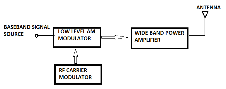
Here, the modulation is done at low power level.
A very small power is associated with the carrier and modulating signal.
The output power of modulation is also low.
Hence wide band power amplifiers are required to boost the amplitude modulated signal upto the desired output level.
Therefore, these systems are known as low level modulators.
High level modulation
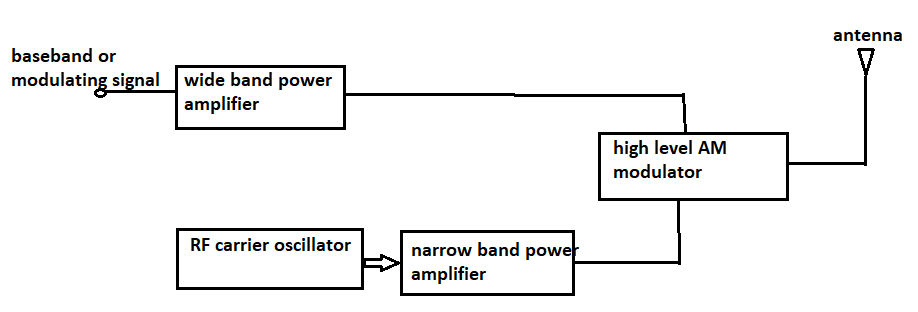
Here, the modulation is done at high power level.
Therefore, to produce amplitude modulation the baseband and the carrier signals are first power amplified and then applied to AM high level modulator.
For base band signal, wide band power amplifier is required to preserve all the frequency components present in the modulating signal.
For carrier signal, narrow band power amplifier is required as it is a fixed frequency signal.
- It stands for Double side band suppressed carrier.
- The AM signal is given by,

- The above signal has three components: unmodulated carrier, LSB and USB.
- The power relation is given by,


When modulation index m =1 then

- Thus two-third of total AM power is utilized for the transmission of carrier component which does not have any message.
- A significant saving of power can be achieved by supressing the carrier before transmission which led to the first variant of basic AM termed as double sideband suppressed carrier (DSBSC) technique.
- The instantaneous voltage of DSBSC may be related to that of AM as


Fig. 5 Amplitude of DSBSC wave (ref 3)
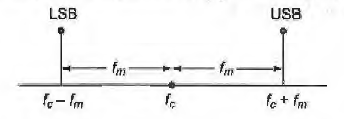
Fig. 6 Frequency spectrum of DSBSC wave (ref 3)
Numerical: (ref 3)

- It is termed as Single sideband suppressed Carrier.
- Here, only one of the side bands is selected for transmission and it needs a bandwidth equal to that of the message.

Where, fm is the maximum frequency component in the message.
- The DSBSC signal is given by,

If LSB is chosen for transmission then

Alternatively if USB is chosen for transmission then

- As compared to AM and DSBSC, SSB saves power since carrier and one sideband are suppressed and saves bandwidth therefore only one sideband is chosen for transmission.
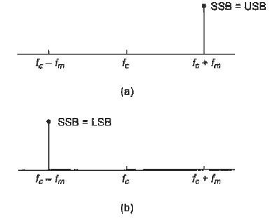
Fig. 7 Frequency spectrum of SSB wave (ref 3)
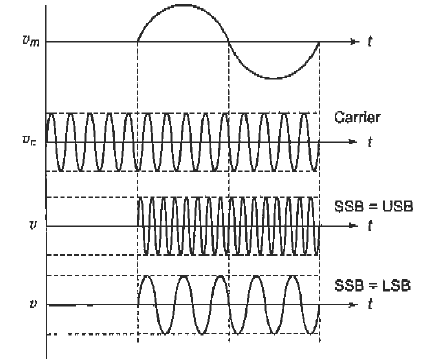
Fig. 8 time domain representation of SSB wave (ref 3)
Numerical: (ref 3)

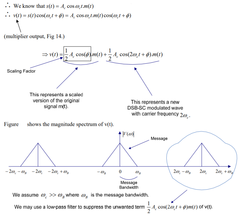
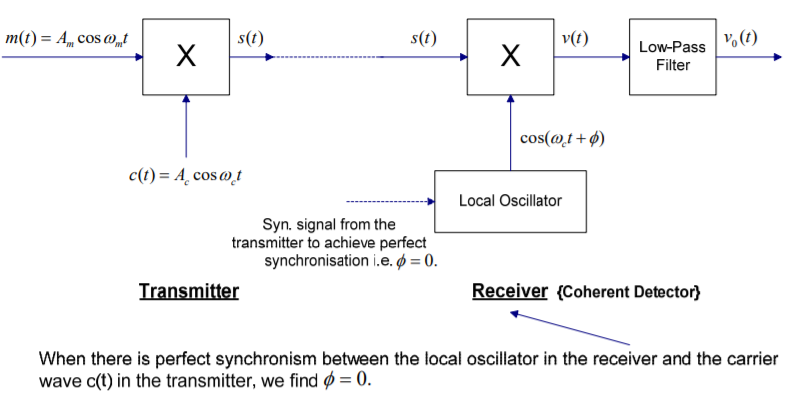
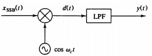
The message signal m(t) can be recovered from a DSB-SC modulated wave s(t) with the help of a locally generated sine wave and then passing through a low-pass filter.
The local oscillator’s output is synchronised, in both frequency and phase with the carrier wave c(t) and is used in the product modulator to generate s(t).
This method of demodulation is called “Coherent Detection”.
Now, the pass-band of the low-pass filter is extended over the entire message spectrum and must satisfy two requirements:
1. Cutoff frequency : ωB
2. Transmission band : ωB ≤ ω ≤ 2 ωc −ωB
Thus the overall output is given by

Numerical:
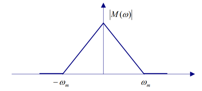
Consider a message signal m(t) with spectrum shown below. The message bandwidth is wm = 2∏ * 103 rad/sec.
This signal is applied to a product modulator, together with a carrier wave , Ac cos(ωc*t) producing the DSB-SC modulated signal s(t). The modulated signal is next applied to a coherent detector. Assuming perfect synchronism between the carrier waves in the modulator and detector, determine the spectrum of the detector output when :
(a) The carrier frequency ωc =2.5∏ * 103 rad/sec.
(b) The carrier frequency. ωc =1.5 π × 103 rad/sec
What is the lowest carrier frequency for which each component of the modulated signal s(t) is uniquely determined by m(t) ?
Solution:
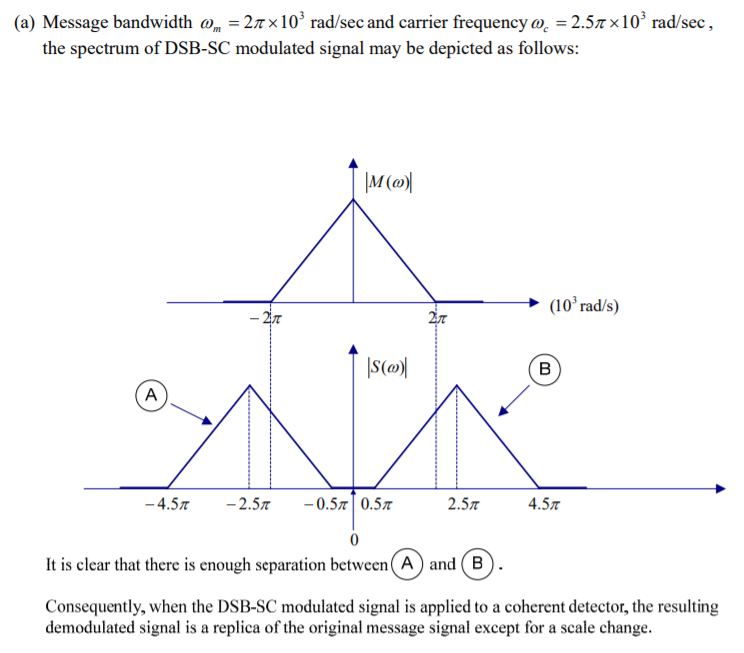
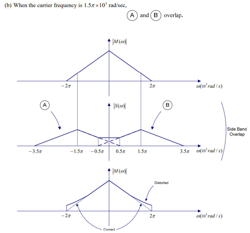
The spectrum of demodulated signal appears at the output of the detector.
There is a distortion in the message signal.
To avoid this, we must choose the carrier frequency in accordance with the condition ωc ≥ ω m .
The minimum acceptable value of ωc is therefore ω m For ωc < ω m , we have sideband overlap and therefore message distortion.
Rectifier circuit gives average value of input signal; but practicsally peak value of input signal is required.
This can be achieved by peak detector circuit.
The figure shows a simple peak detector circuit using diode and capacitor.
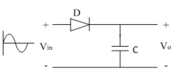
In the positive half cycle, diode D is forward biased and capacitor C begins to charge. When input voltage reaches its peak value, capacitor gets charged to positive peak value.
In negative half cycle, as input voltage decreases, diode D becomes reverse biased and capacitor remains isolated and holds the peak value of previous cycle.
Hence called as peak detector.
But practically, output is taken across some load RL, hence as input voltage decreases capacitor discharges through load RL.
To avoid this, RL is kept at a very large value so that capacitor discharges slowly hence almost holds the charge. Whatever charge it lost through RL is again achieved back in next half cycle.
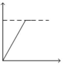
Here, the diode D is acts as an instant switch, so supply gets loaded.
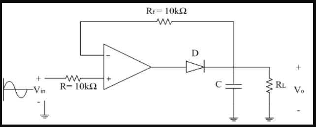
To avoid loading effect while charging capacitor, we use op-amp.
Op-amp is placed between input and diode D so loading is avoided as shown below,
The process of extracting an original message signal from DSBSC wave is known as detection or demodulation of DSBSC. The following detectors are used for demodulating DSBSC wave.
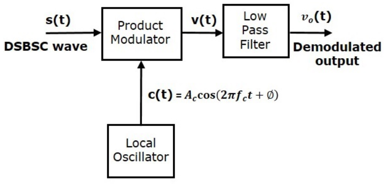
Here, the message signal can be obtained from DSBSC wave by multiplying it with a carrier having the same frequency and the phase in the product modulator. The signal is then passed through a Low Pass Filter and the desired message signal is obtained.
Let the DSBSC wave be
s(t)=Ac cos(2πfct) m(t)s(t)
=Ac cos(2πfct) m(t)
The output of the local oscillator is
c(t)=Ac cos(2πfct+ϕ) c(t)=Ac cos(2πfct+ϕ)
Where, ϕ is the phase difference between the oscillator signal and the carrier signal, that is used for DSBSC modulation.
From the figure, we can write the output of product modulator as
v(t)=s(t)c(t)v(t)=s(t)c(t)
Substitute, s(t) and c(t) values in the above equation.
⇒v(t)=Accos(2πfct)m(t)Accos(2πfct+ϕ)⇒v(t)=Accos(2πfct)m(t)Accos(2πfct+ϕ)
=Ac cos(2πfct)cos(2πfct+ϕ)m(t)=Ac cos(2πfct)cos(2πfct+ϕ)m(t)
=Ac [cos(4πfct+ϕ)+cosϕ]m(t)=Ac [cos(4πfct+ϕ)+cosϕ]m(t)
v(t)=Ac cosϕm(t)+Ac cos(4πfct+ϕ)m(t)v(t)
=Ac cosϕm(t)+Ac cos(4πfct+ϕ)m(t)
Here, the first term is the scaled version of the message signal. It can be obtained by passing the above signal through a low pass filter.
Therefore, the output of low pass filter is
v0t=Ac cosϕ m(t) v(t)=Ac cosϕm(t)
The demodulated signal amplitude will be maximum, when ϕ=0. Therefore, the local oscillator signal and the carrier signal should be in phase, i.e., there should not be any phase difference between these two signals.
The demodulated signal amplitude remains zero, when ϕ=±90.
This effect is known as quadrature null effect.
1. Synchronous Detector
2. Phase shift detector
References:
- Communication system by Bruce carison . TMH.
- Electronic Communication system by Kennedy IV Edition. TMH.
- Electronic Communication system by Roddey & Coolen, Pearson.
- Telecommunication system Engg. By Freeman John Wiley
- Communication system by Haykin,Wiley