Unit – 1
DC Circuits
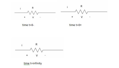
# In case of capacitor: -
At time t= 0-

:. Capacitor is initially uncharged
Q (0-) =0
Q=cv
Q (0-) = cvc (0-)
Vc (0-) =0
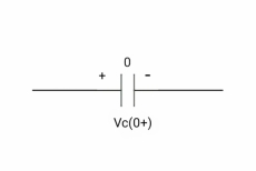
At time t= 0+
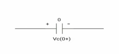
By low of conservation of charges
Q (0-) = Q (0+)
Cvc (0-) =cvc (0+)
Vc (0+) =0
Hence acts as

If capacitor is initially uncharged at t= 0- than voltage across capacitor is zero at t=0+ capacitor will follow low of conservation of charges and Vc (0+) =0 it means at t=0+ capacitor behaves as short circuit in other words, voltage across capacitor cannot change instantaneously.
At time t= infinity,
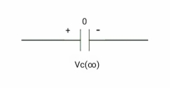

I = cdvc/dt constant and maximum
hence, i= 0
At t= infinity capacitor will be fully charged or voltage across capacitor is constant and current through capacitor is zero so, capacitor will behave as open –circuit
Say capacitor is initially charged
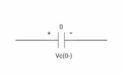
at time t= 0-,

at time t= 0+,
at time t= 0+

Q (0-) = Q (0+)
Cvc (0-) =cvc (0+)
V1 = Vc (0+)

Hence acts as

Its capacitor is initially charged at t= 0- as voltage across capacitor is V1 than at t=0+ capacitor behaves as a voltage as a voltage source with value V1
At time t = infinity
If capacitor is initially charged and it is connected to any independent source for long time than current through capacitor is 3 etw and capacitor will be fully charged and it behaves as o.c
# for Inductor: -
At time t= 0-

Ø= Li =0
Ø (0) = Li (0-)
i (0-) =0
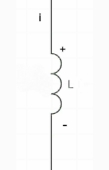
at t= 0+,
By low of conservation of flux
Ø (0-) = Ø (0+)
Li (0-) = Li (0+)
0 =i (0+)
Hence, acts as short circuit
Ideal and practical Voltage and Current source:
A voltage source is a device which provides a constant voltage to load at any instance of time and is independent of the current drawn from it. This type of source is known as an ideal voltage source. Practically, the ideal voltage source cannot be made. It has zero internal resistance. It is denoted by this symbol.
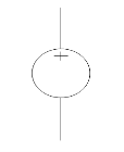
Fig: Voltage source symbol
Ideal Voltage Source
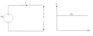
Fig: Ideal Voltage Source
The graph represents the change in voltage of the voltage source with respect to time. It is constant at any instance of time.
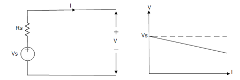
Voltage sources that have some amount of internal resistance are known as a practical voltage source. Due to this internal resistance, voltage drop takes place. If the internal resistance is high, less voltage will be provided to load and if the internal resistance is less, the voltage source will be closer to an ideal voltage source. A practical voltage source is thus denoted by a resistance in series which represents the internal resistance of source.
Practical Voltage source
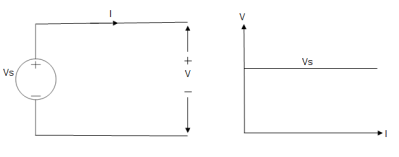
Fig: Practical Voltage source
The graph represents the voltage of the voltage source with respect to time. It is not constant but it keeps on decreasing as the time passes.
Current source
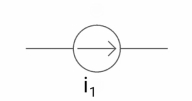
A current source is a device which provides the constant current to load at any time and is independent of the voltage supplied to the circuit. This type of current is known as an ideal current source; practically ideal current source is also not available. It has infinite resistance. It is denoted by this symbol.
Ideal Current source
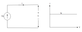
Fig: Ideal Current source
The graph represents the change in current of the current source with respect to time. It is constant at any instance of time.
Why ideal Current source has infinite resistance?
A current source is used to power a load, so that load will turn on. We try to supply 100% of the power to load. For that, we connect some resistance to transfer 100% of power to load because the current always takes the path of least resistance. So, in order for current to go to the path of least resistance, we must connect resistance higher than load. This is why we have the ideal current source to have infinite internal resistance. This infinite resistance will not affect voltage sources in the circuit.
Practical Current source
Practically current sources do not have infinite resistance across there but they have a finite internal resistance. So the current delivered by the practical current source is not constant and it is also dependent somewhat on the voltage across it.
A practical current source is represented as an ideal current source connected with resistance in parallel.
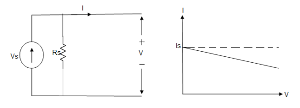
Fig; Practical Current source
The graph represents the current of the current source with respect to time. It is not constant but it also keeps on decreasing as the time passes.
Examples of current and voltage sources
The examples of current source are solar cells, transistors and examples of some voltage sources are batteries and alternators.
This was all about ideal and practical sources of power. The ideal sources are very useful for calculations in theory but as ideal sources are not practically possible, only practical sources are used in practical circuits. The batteries we use are a practical source of power and the voltage and current decreases as we use it. Thus both are useful to us in their own ways.
The algebraic sum of currents meeting at a junction or node in a electric circuit is zero or the summation of all incoming current is always equal to summation of all outgoing current in an electrical network.
Explanation
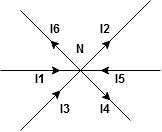
Assuming the incoming current to be positive and outgoing current negative we have


I e incoming current = ∑ outgoing current thus, the above Law can also be stated as the sum of current flowing towards any junction in an electric circuit is equal to the sum of currents flowing away from that junction
Kirchhoff’s Voltage Law (KVL)
Kirchhoff’s Voltage Law or KVL, states that “in any closed loop network, the total voltage around the loop is equal to the sum of all the voltage drops within the same loop” which is also equal to zero. In other words, the algebraic sum of all voltages within the loop must be equal to zero.
By convention
Apply the polarity sign which is attached to the entering point of the device.
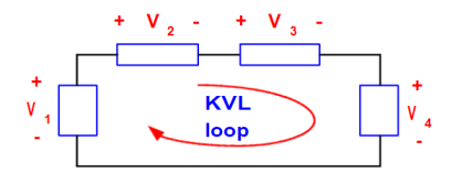
We apply the sign of the device that the loop first touches.
-V1 + V2 + V3 + V4 =0
V1 = V2 + V3 + V4
4
1234
0
Here is a simple circuit with DC excitation:
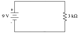
Analysis would mean we determine the voltages at all the nodes and currents in all the branches of this circuit.
A node is defined as any point where two or more components meet.
A branch is defined as any path between two nodes.
Let’s label all the nodes in the circuit above:
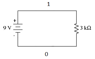
We have only two nodes here, ‘1’ and ‘0’.
We call node ‘0’ the ground node. The ground node is at 0 volt.
Node ‘1’ is connected to the top of our DC voltage source. So it is at 9 volts.
Half our job is done here, because we now know the voltages at all the nodes in our circuit.
Next, let’s talk about the branches.
There are two branches in our circuit. One branch contains the 9V DC source and the other branch contains the 3k resistor.
We know find the currents through the branches.
From Ohm’s law we can calculate the current in the resistor.
I = V/R
This gives us a current of 9/3k = 3 mA.
The current in the resistor branch is 3 mA. And, because our circuit is one single closed loop, this current also flows in the other branch.
At this point, we know all the voltages at each node and the currents through each branch of our simple circuit. So, we say that the analysis of our simple DC excitation circuit is complete.
Star to delta conversion to final equivalent resistance
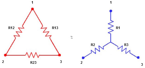
We know that (from delta to star conversion)
R1 =  …….①
…….①
R2 =  …..②
…..②
R1 =  ……③
……③
Multiply ① X ② L.H.S and R.H.S
R1 R2 =  …….④ where
Similarly multiply ② X ③
R2 R3 =  …….⑤
…….⑤
And ③ X①
R1 R3 =  …….⑥
…….⑥
Now add equation ④, ⑤, and ⑥ L.H.S and R.H.S


 ……refer eq. ②
 =
=  +
+  +
+ 
 =
=  +
+ 
 (Delta)
 star star
Similarly R23 = R2+R3 + 
R23 = R1+R2 + 
Delta to Star Conversion to Find (Req.)
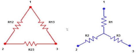
Delta  Star
Star
= R12// (R23 + R13) =R1 + R2
= 
 = R1 + R2
= 

Here let R = R12 + R23 + R13
= 
 R2 + R3

 R1 + R3
Now the 3 equations after equating L.H.S. and R.H.S
R1 + R2 =  …….①
…….①
R2 + R3 =  ……②
……②
R1 + R3 =  …..③
…..③
Now subtract ② and ① on L.H.S. and R.H.S
R2+ R3 – R1 – R2 = 
 R3 – R1 =
  …..④
…..④
Now add equation ④ and ③
R3 – R1 + R1 + R3 = 
2R3 = 

Similarly R1 = 
And R2 = R23 R12/R where R = R12 + R23 + R13
ie star equivalent from delta network is ratio of product of adjacent branches in delta to the addition of all branches in delta.
Superposition Theorem
Superposition theorem states that in any linear, active, bilateral network having more than one source, the response across any element is the sum of the responses obtained from each source considered separately and all other sources are replaced by their internal resistance. The superposition theorem is used to solve the network where two or more sources are present and connected.
If a number of voltage or current sources are acting in a linear network, the resulting current in any branch is the algebraic sum of all the currents that would be produced in it when each source acts alone while all the other independent sources are replaced by their internal resistances.
Using Superposition theorem determine the voltage drop and current across the resistor 3.3K as shown in figure below
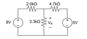
Step 1:
Remove 8V power supply from the original circuit such that the new circuit becomes as the following and measure the voltage across resistor.
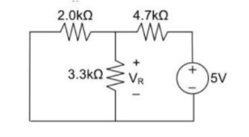
Here 3.3 K and 2K are in parallel therefore the resultant resistance will be 1.245K
Using voltage divider rule across 1.245K will be
V1 =[1.245/(1.245+4.7)] * 5 = 1.047V
Step 2:
Remove the 5V power supply from the original circuit such that the new circuit becomes the following and then measure the voltage across resistor.
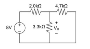
Here 3.3K and 4.7K are in parallel therefore the resultant resistance will be 1.938K. Using voltage divider rule voltage across 1.938K will be
V2 =[1.938(1.938+2)] *8 = 3.9377V
Therefore, voltage drop across 3.3K resistor is V1+V2 = 1.047 + 3.9377 = 4.9847V
Thevenin’s and Norton’s Theorem
Thevenin’s Theorem states that “Any linear circuit containing several voltages and resistances can be replaced by just one single voltage in series with a single resistance connected across the load”.
For the circuit as shown in figure find the current through RL = R2 = 1Ω resistor (Ia-b) branch using Thevenin’s theorem. Find the voltage across the current source.
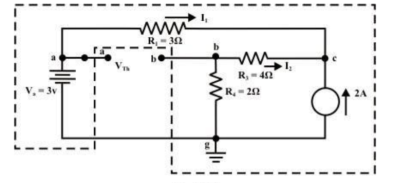
Step 1: Disconnect the load resistance and reconnect the circuit.
Step 2: Apply any method to calculate Vth
At node C
2 + I1 + I2 =0
2 + (3 -Vc)/3 + (0-Vc/6) -- Vc = 6V
The currents I1 and I2 are computed by the following expressions:
I1 = Va -Vc/3 = 3-6/3 = -1A (I1 is flowing from c to a)
I2 = 0 – Vc/6 = -6/6 = -1A (I2 is flowing from c to a)
Step-3:
Redraw the circuit indicating the direction of currents in different branches. One can find the Thevenin’s voltage VTh using KVL around the closed path ‘gabg’
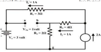
VTh = Vag − Vbg = 3 − 2 =1volt
Step 4:
Replace all sources by their internal resistances. In this problem, voltage source has an internal resistance zero (0) (ideal voltage source) and it is short-circuited with a wire.
On the other hand, the current source has an infinite internal resistance (ideal current source) and it is open-circuited (just remove the current source).
Thevenin’s resistance RTh of the fixed part of the circuit can be computed by looking at the load terminals ‘a’- ‘b’
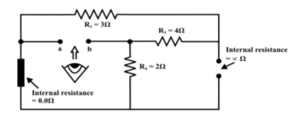
RTh = ( R1 + R3 ) & R4 = ( 3 + 4 )&2 = 1.555Ω
Step-5: Place RTh in series with VTh to form the Thevenin’s equivalent circuit. Reconnect the original load resistance RL = R2 = 1 Ω to the Thevenin’s equivalent circuit.
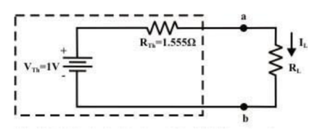

Step-6: The circuit is redrawn to indicate different branch currents. Referring to one can calculate the voltage Vbg and voltage across the current source (Vcg ) using the following equations.
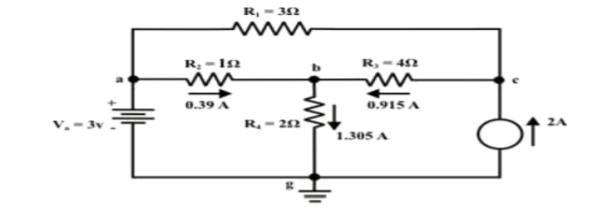
Vbg = Vag − Vab = 3 − 1 × 0.39 =2.61 volt.
Ibg = 2.61 2 = 1.305 A;
Icb = 1.305 − 0.39 = 0.915 A
Vcg = 4 × 0.915 + 2 ×1.305 =6.27 volt.
For the circuit shown in figure, find the current IL through 6 Ω resistor using Thevenin’s theorem.

Step-1:
Disconnect 6 Ω from the terminals ‘a’ and ‘b’ and the corresponding circuit diagram. Consider point ‘g’ as ground potential and other voltages are measured with respect to this point.
Step-2:
Apply any suitable method to find the Thevenin’s voltage (VTh )
KVL is applied around the closed path ‘gcag’ to compute Thevenin’s voltage.
42 – 8I – 4I -30 = 0 ; I = 1A
Vag = 30+4 = 34 volt
Vbg = 2 x 3 = 6 volt
Vth = Vab = Vag – Vbg = 34 -6 = 28 volt
Step-3:
Thevenin’s resistance RTh can be found by replacing all sources by their internal resistances all voltage sources are short-circuited and current sources are just removed or open circuited.
Rth = (8 x4) / 12 + 2 = 14/3 = 4.666Ω
Step-4:
Thevenin’s equivalent circuit is now equivalently represents the original circuit

IL = Vth / Rth + RL = 28 / 4.666 +6 = 2.625 A
Norton’s Theorem
Norton’s Theorem states that “Any linear circuit containing several energy sources and resistances can be replaced by a single Constant Current generator in parallel with a Single Resistor”.
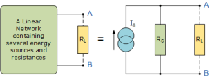
Problem:
Find RN, IN, the current flowing through and load Voltage across the load resistor in fig (1) by using Norton’s Theorem.

Step 1:
Short the 1.5 Ω load resistor.
Step 2:
Norton current.
Short AB terminals to obtain IN . The total resistance of the circuit is
2Ω + (6Ω || 3Ω)
RT = 4 Ω
IT = V / RT = 12/ 4 = 3 A
IN = 3 A x [ 6Ω / 3 + 6 )] = 2A
IN = 2A
Step 3:
Open current sources, Short Voltage sources and Open Load resistor.
Step 4:
Calculate Norton Resistance (RN)
Reduce 12V dc source. 3Ω resistor is in series with combination of 6Ω and 2Ω resistor
3Ω + (6Ω||2Ω)
3Ω + 1.5 Ω = 4.5 Ω; RN = 4.5 Ω
Step 5:
Connect RN in parallel with current source IN and the load resistor.
Step 6:
The load current through Load resistor
IL = IN x [ RN /(RN + RL)
=2 A x ( 4.5 / 4.5 + 1.5 K) = 1.5 A
IL = 1.5 A
The voltage across load resistor
VL = IL x RL
= 1.5 x 1.5
VL = 2.25 V
Maximum power transfer theorem states that AC voltage source will deliver maximum power to the variable complex load only when the load impedance is equal to the complex conjugate of source impedance.
Proof:
Replace any two terminal linear network or circuit to the left side of variable load resistor having resistance of RL ohms with a Thevenin’s equivalent circuit. We know that Thevenin’s equivalent circuit resembles a practical voltage source.
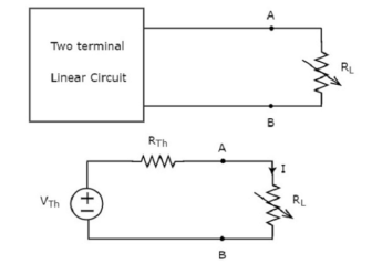
The amount of power dissipated across the load resistor is
PL = I 2 R L ----------------------(1)
Substitute I = Vth / Rth + RL
PL = Vth / (Rth + RL ) 2 RL
PL = Vth 2 { RL / (RTH + RL) 2 ------------------------------(2)
Condition for Maximum Power Transfer
For maximum or minimum, first derivative will be zero. So, differentiate Equation 1 with respect to RL and make it equal to zero.
dPL / d RL = V Th 2 { (Rth + RL) 2 x 1 -RL x 2(Rth + RL) / (Rth + RL) 4 } =0
(Rth + RL) 2 – 2RL (Rth + RL) = 0
(Rth + RL) (Rth + RL – 2 RL) = 0
Rth - RL = 0
Rth = RL or RL = Rth
Therefore, the condition for maximum power dissipation across the load is RL=RTh. That means, if the value of load resistance is equal to the value of source resistance that is Thevenin’s resistance, then the power dissipated across the load will be of maximum value.
Substitute RL = Rth and PL = PL,max
PL,max = V th 2 { Rth / (Rth + Rth ) 2 }
= V th 2 ( Rth / 4 Rth 2 )
= V th 2 / 4 Rth
PL,max = V th 2 / 4 RL [RL = Rth]
Efficiency of Maximum power transfer
 = PL,max/ Ps
PL,max = maximum amount of power transferred to the load
Ps = amount of power generated by the source.
The amount of power generated by the source is
Ps = I2 Rth + I2 RL
Ps = 2 I2 Rth ; since RL = Rth
Substitute I = Vth / 2 Rth
Ps = 2(Vth / 2Rth) 2 Rth
Ps = 2(Vth / 4Rth) 2 Rth
Ps = Vth 2 / 2 Rth
Substituting with PL max and Ps
 = (Vth 2 / 4 Rth) / (Vth 2 / 2 Rth)
 max = ½
Problem:
Find the maximum power that can be delivered to the load resistor RL of the circuit shown in the following figure.

Step 1 – Using Thevenin’s circuit we get
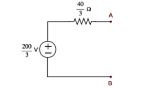
Thevenin’s voltage Vth = 200/3 and Thevenin’s resistance Rth = 40/3
Step 2 – Replace the left side of terminals A & B of the given circuit with the above Thevenin’s equivalent circuit. The resultant circuit diagram will be
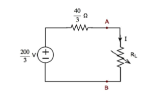
Step 3 − We can find the maximum power that will be delivered to the load resistor, RL by using the following formula.
P L,max = Vth 2 / 4 Rth
Substitute VTh=200/3 and RTh=40/3Ω
P L,max = (200/3) 2 / 4 (40/3)
Therefore, the maximum power that will be delivered to the load resistor RL of the given circuit is 250/3 .
Problem:
For the circuit shown find the value of RL that absorbs maximum power from the circuit and the corresponding power under this condition.
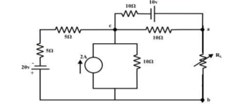
Load resistance RL is disconnected from the terminals ‘a’ and ‘b’ and the corresponding circuit diagram.
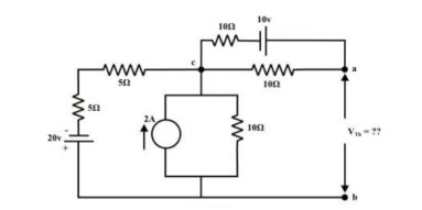
The above circuit is equivalently represented by a Thevenin circuit and the corresponding Thevenin voltage VTh and Thevenin resistance RTh are calculated by following the steps given below:
Considering 20V only
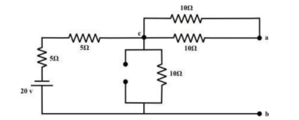
From the above circuit the current through ‘b-c’ branch =20/ 20 = 1𝐴 (𝑓𝑟𝑜𝑚 𝑎 𝑡𝑜 𝑏). whereas the voltage across the ‘b-a’ branch vba =1 ×10 =10 volt . Since ’b’ is higher potential than ‘a’ ∴vab = − 10volt.
Considering only 10v source only
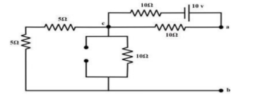
No current is flowing through ‘cb’-branch. Vab = 5v (‘a’ is higher potential than ‘b’). Consider only 2 A current source only
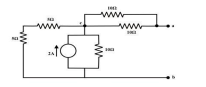
To compute Rth
Replace all voltage and current sources by their internal resistance of the circuit.
Rth = Rab = ((5+5)||10) + (10||10) = 5+5 =10Ω
RL = Rth = 10Ω
The maximum power dissipated to RL is
Pmax = Vth 2 / 4 Rth = ¼ 25 /10 = 0.625 watts
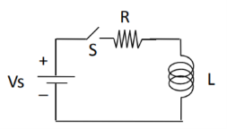
Fig. shows a series RL circuit connected across a DC source through a switch S.
When switch ‘S’ is close at t>0 the as per KVL network equation will be …

The above equation is non homogenous equation linear differential equation of first order.
The solution of Eq. 1 will give i(t) which consists of two components i.e.
Complimentary function in(t) which will satisfy di(t)/dt + R/L i(t) =0 -------------(1)
Particular integral if(t) which will satisfy R i(t) + L di(t)/dt = Vs ------------------(2)
Since I is constant
L dI/dt =0
if(t) = I = Vs /R
i(t) = Io e –(R/L) t = Io e –(t/ ) -------------------------------(3)
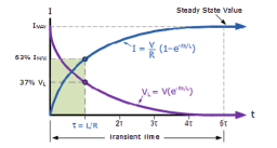
where  time constant of RL circuit.
Eq(3) provides the natural reproduced and is reproduced below…….
in(t) = K e –(R/L) t = K e –(t/τ) ---------------------------------(4)
Eq(1) can be written with i(t) = I constant
RI + L dI/dt = Vs
Since I = constant
L dI/dt =0
if(t) = I = Vs/R
Substitute Eq. 4 & Eq.6 in Eq.2 yields the solution of Eq. 1
We get….
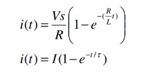
i(t) = K e -t/τ + Vs/R = K e -t/τ + I where K is determined from initial condition that is t=0--- Eq 7 will be
K = -Vs/R = - I …………………………..(8)
Hence complete solution of eq (1) is given by
RC series
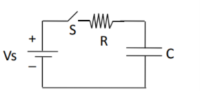
The figure shows a series RC circuit connected across a DC source through a switch S. It is assumed that capacitor voltage id V0 When switch ‘S’ is close at t>0 the as per KVL network equation will be …
Vs – R i(t) – vc(t) =0 --------------------------------(9)
For analysis of circuit of Fig. 2 the capacitor voltage Vc(t) is chosen as variable.
Substituting i(t) = c dvc(t)/dt in Eq. 9 We get.
RC dvc(t) /dt + vc(t) = Vs for t>0 ---------------------------------(10)
Above eq.10 like eq1 it is non homogeneous equation linear differential equation of first order. Therefore solution is
Vc(t) = k e -t/τ + V --------------------------------------------------------------------------(11)
In Eq. 11 the time constant is By substituting initial condition Eq. 11 i.e. Vc = V0 it leads to By substituting value of K in Eq. 11 and after simplification we get …
Vc(t) = Vo e (-t/τ) + Vs ( 1 – e -t/τ) for t>0
The expression for current in the circuit is given by ………………
i(t) = C dvc(t)/dt
i(t) = C[ (-1/τ Vo e –(t/τ) + ( 1/τ Vs e –(1/τ)]
i(t) = C / RC (Vs-Vo) e -t/ τ ---------------------------------------------(12)
i(t) = (Vs-Vo) / R e -t/τ ----------------------------------------------(13)
References: