Unit -2
Combinational Digital Circuits
- It deals with binary numbers & variables.
- Therefore, also known as Binary Algebra or logical Algebra.
- A mathematician named as George Boole had developed this algebra in 1854.
- The variables that are used in this algebra are known as Boolean variables.
- Considering the range of voltages as logic ‘High’ is represented with ‘1’ and logic ‘Low’ is represented with ‘0’.
Boolean Postulates
- Considering the binary numbers 0 and 1, boolean variable (x) and its complement (x’).
- They known as literal.
- The possible logical OR operations are:
x + 0 = x
x + 1 = 1
x + x = x
x + x’ = 1
- Similarly, the possible logical AND operations are:
x.1 = x
x.0 = 0
x.x = x
x.x’ = 0
- These are the simple Boolean postulates and verification can be done by substituting the Boolean variable with ‘0’ or ‘1’.
Key Takeaways:
- The range of voltages as logic ‘High’ is represented with ‘1’ and logic ‘Low’ is represented with ‘0’.
- Logical OR is summing of the literals and logical AND is multiplication of the two literals.
Simplifying K-maps:
- Selecting K-map on the basis of number of variables present in the Boolean function.
- If the Boolean function is in Max terms form, then place the zeroes at respective Max term cells in theK-map.
- If the Boolean function is in PoS form, then place the zeroes wherever required in K-map for which the given sum terms are valid.
- The maximum possibilities of grouping is checked for adjacent zeroes.
- It should be of powers of two.
- Starting from highest power of two and to the least power of two.
- Highest power is equivalent to the number of variables considered in K-map and least power is zero.
- Each group will give either a literal or one sum term.
- It is known as prime implicant.
- The prime implicant is an essential prime implicant when at least a single ‘0’ is not covered with any other groups but only that grouping covers.
- The simplified Boolean function contains all essential prime implicants and only the required prime implicants.
The process of simplifying the algebraic expression of a boolean function is called minimization. Minimization is important since it reduces the cost and complexity of the associated circuit.
For example, the function can be minimized. The circuits associated with above expressions is –
It is clear from the above image that the minimized version of the expression takes a less number of logic gates and also reduces the complexity of the circuit substantially.
Minimization is hence important to find the most economic equivalent representation of a Boolean function.
Minimization can be done using Algebraic Manipulation or K-Map method. Each method has it’s own merits and demerits.
- Karnaugh introduced a method for simplification of Boolean functions in an very easy way.
- This method is known as Karnaugh map method or K-map method.
- It is a graphical method, which comprises of 2n cells for ‘n’ variables.
- Here, the adjacent cells varies only in single bit position.
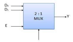
- It is a special type of combinational circuit.
- It has n-data inputs, one output and m inputs select lines with 2m = n.
- It selects one of the n data inputs and routes it to the output.
- The selection of one of the inputs is done by the select lines.
- Depending on the code applied at the inputs, one of the n data sources is selected and transmitted to the single output Y.
- E is the enable input which is useful for cascading purpose.
- It is an active low terminal hence performs the required operation when it is low.
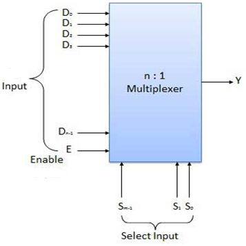
Block diagram of multiplexer
Multiplexers come in multiple variations
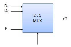
- 2 : 1 multiplexer
- 4 : 1 multiplexer
- 16 : 1 multiplexer
- 32 : 1 multiplexer
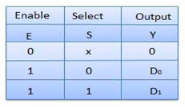
Block Diagram of 2:1 MUX
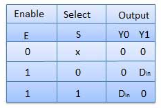
Truth Table of 2:1 MUX
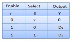
Where x is don’t care.
Key Takeaways
- It has n-data inputs, one output and m inputs select lines with 2m = n.
- The selection of one of the inputs is done by the select lines.
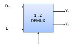
DE- MULTIPLEXER
- It performs the inverse operation of a multiplexer as it receives one input and distributes it across its outputs.
- It has only one input and n outputs with m select input.
- At a time only one output line is selected by the select lines and that input is transmitted through the output line.
- It is equivalent to a single pole multiple way switch .
Various Demultiplexers are used as:
- 1 : 2 demultiplexer
- 1 : 4 demultiplexer
- 1 : 16 demultiplexer
- 1 : 32 demultiplexer
Block diagram

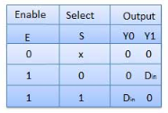
Truth Table
Where x is don’t care.
Key Takeaways:
- It performs the inverse operation of a multiplexer as it receives one input and distributes it across its outputs.
- It has only one input and n outputs with m select input.
- Half Adder
It is a combinational circuit which has two inputs and two outputs.
It is designed to add two single bit binary number A and B.
It has two outputs carry and sum.
Block diagram
Half adder
Truth Table
Circuit Diagram
Half adder
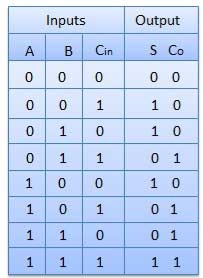
Full Adder
- It is developed to overcome the drawback of Half Adder circuit.
- It can add two one-bit numbers A and B and a carry C.
- It is a three input and two output combinational circuit.
Block diagram
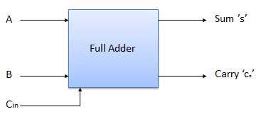
Full adder
Truth Table

Circuit Diagram

Full adder
Key Takeaways:
- Half adder is a combinational circuit which has two inputs and two outputs.
- Since there is no provision for carry in half adder, full adder is developed to overcome the drawback.
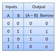
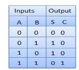
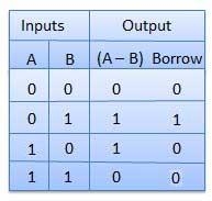
Subtractor
- Half Subtractors
It is a combination circuit with two inputs and two outputs.
The difference between the two binary bits is obtained at the output and an output (Borrow) indicates if a 1 has been borrowed.
Here A is called as Minuend bit and B is called as Subtrahend bit.
Truth Table
Circuit Diagram
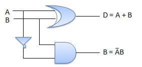
Half subtractor
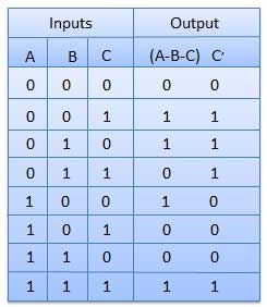
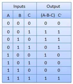
B. Full Subtractors
It is a combinational circuit which has three inputs A,B,C and two output D and C'.
A is the 'minuend', B is 'subtrahend', C is the 'borrow' which is produced by the previous stage, difference output D and C' is the borrow output.
Truth Table
Circuit Diagram
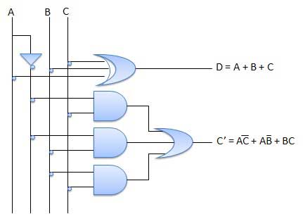
Full subtractor
Key Takeaways:
- Half subtractor is a combinational circuit which has two inputs and two outputs.
- Since there is no provision for borrow in half subtractor, full subtractor is developed to overcome the drawback.
A decimal number contains 10 digits (0-9). Now the equivalent binary numbers can be found out of these 10 decimal numbers. In case of BCD the binary number formed by four binary digits, will be the equivalent code for the given decimal digits. In BCD we can use the binary number from 0000-1001 only, which are the decimal equivalent from 0-9 respectively.
Let, (12)10 be the decimal number whose equivalent Binary coded decimal will be 00010010. Four bits from L.S.B is binary equivalent of 2 and next four is the binary equivalent of 1.
BCD Addition
Example 1
Let, 0101 is added with 0110.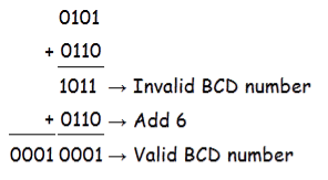
Check your self.
Example 2
Let 0001 0011 is added to 0010 0110.

So no need to add 6 as because both  are less than (9)10.
This is the process of BCD Addition.
BCD Subtraction
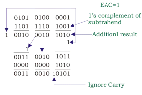
Example: – 1
Let 0010 0001 0110 is subtracted from 0101 0100 0001.
- At first 1’s compliment of the subtrahend is done, which is 1101 1110 1001 and is added to 0101 0100 0001. This step is called adder 1.
- Now after addition if any carry occurs then it will be added to the next group of numbers towards MSB. Then EAC will be examined. Here, EAC = 1. So the result of addition is positive and true result of adder 1 will be transferred to adder 2.
- Now notice from LSB. There are three groups of four bit numbers. 1010 is added 1011 which is the first group of numbers because it do not have any carry. The result of the addition is the final answer.
- Carry 1 will be ignored as it is from the rule.
- Now move to the next group of numbers. 0000 is added to 0010 and gives the result 0010. It is the final result again.
- Now again move to the next group here 0000 is also added to 0011 to give the final result 0011.
- You may have noticed that in this two groups 0000 is added, because result of first adder do not contain any carry. Thus the results of the adder 2 is the final result of BCD Subtraction.
Therefore, 
Check.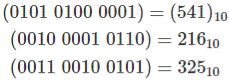
We know that 541 − 216 = 325, Thus we can say that our result of BCD Subtraction is correct.
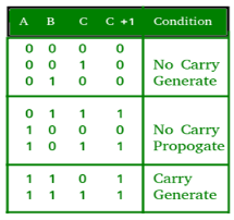
- In this, for each adder block, the two bits that are to be added are available instantly.
- However, each of them waits for the carry to arrive from the previous one.
- So, it is impossible to generate the sum and carry of any block until the input carry is known.
- The block waits for the previous block to produce its carry. So there will be a considerable time delay which is known as carry propagation delay.
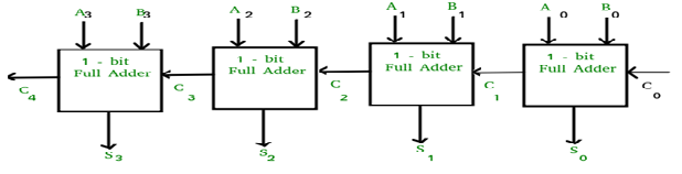
- Here, the sum is produced by the corresponding full adder as soon as the input signals are applied to it. The carry must propagate to all the stages so that output and carry settle their final steady-state value.
- The propagation time is equal to the propagation delay of each adder block, multiplied by the number of adder blocks in the circuit.
- It reduces the propagation delay by introducing more complex hardware.
- The ripple carry design is suitably transformed in such a way that the carry logic over fixed groups of bits is reduced to two-level logic.
Look ahead Carry adder
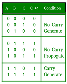
Advantages and Disadvantages of Carry Look-Ahead Adder :
Advantages –
- The propagation delay is reduced.
- It provides the fastest addition logic.
Disadvantages –
- The circuit gets complicated as number of variables increase.
- It is costlier as it requires more hardware.
Key Takeaways:
- Here, the sum is produced by the corresponding full adder as soon as the input signals are applied to it. The carry must propagate to all the stages so that output and carry settle their final steady-state value.
- It reduces the propagation delay by introducing more complex hardware.
Serial binary adder is a combinational logic circuit that performs the addition of two binary numbers in serial form. Serial binary adder performs bit by bit addition. Two shift registers are used to store the binary numbers that are to be added.
A single full adder is used to add one pair of bits at a time along with the carry. The carry output from the full adder is applied to a D flip-flop. After that output is used as carry for next significant bits. The sum bit from the output of the full adder can be transferred into a third shift register.
Fig: Block diagram of Serial Binary Adder
- An ALU performs mathematical and logical operations on binary numbers.
- They are located at the heart of every digital computer system and are one of the most important parts of a CPU (Central Processing Unit).
- Fetch-decode-execute refers to a computational process that continuously fetches the instructions from a memory, decodes them into operations and executes them to perform a calculation.
- These are simple steps which give rise to the complex behaviours that we expect from modern computing machines.
An illustration of the fetch-decode-execute cycle
This process can be further explained by linking each cycle step with three hardware subsystems called as a memory unit, a control unit, and an arithmetic unit.
MSI chips have less than 500 components or have more than 10 but less than 100 gates.
Although medium-scale integration has been replaced by other methods for the regular creation of microchips, recent news shows that engineers have been using carbon nanotube methods to develop new kinds of microchips on a medium-scale integration level.
- It performs comparison operation with more than four bits by cascading two or more 4-bit comparators.
- When two comparators are to be cascaded, the outputs of the lower-order comparator is connected to corresponding input of the higher-order comparator.
Digital comparator
Applications of Comparators –
- They are used in central processing units (CPUs) and microcontrollers (MCUs).
- They are used in control applications where the binary numbers represents physical variables such as temperature, position, etc. and are compared with a reference value.
- They are also used as process controllers and Servo motor controllers.
- They are used in password verification and biometric applications too.
- The parity generating technique is used as error detection technique for the data transmission.
- When binary data is transmitted and processed , it is subjected to noise and that noise can alter 0s to 1s and 1s to 0s of data bits in digital systems.
- Therefore, a parity generator is a combinational logic circuit that generates the parity bit at the transmitter end.
- The basic principle is that sum of odd number of 1s is always 1 and sum of even number of 1s is always zero.
- Such error detection and correction can be implemented by using Ex-OR gates.
Even Parity Generator
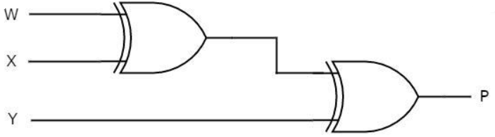
A 3-bit message is transmitted with an even parity bit. Hence assuming, the three inputs W,X and Y that are applied to the circuits and output bit is the parity bit P. The total number of 1s must be even, to generate the even parity bit P.
3- bit message | Even Parity | ||
W | X | Y | P |
0 | 0 | 0 | 0 |
0 | 0 | 1 | 1 |
0 | 1 | 0 | 1 |
0 | 1 | 1 | 0 |
1 | 0 | 0 | 1 |
1 | 0 | 1 | 0 |
1 | 1 | 0 | 0 |
1 | 1 | 1 | 1 |
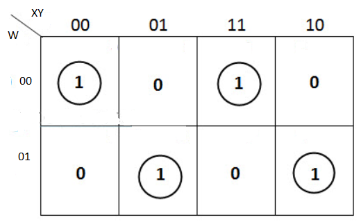
The K-map simplification for 3-bit message even parity generator is
From the above K-Map, the expression is:
P=W′X′Y+W′XY′+WX′Y′+WXY
P=W′(X′Y+XY′)+W(X′Y′+XY)
P=W′(X⊕Y)+W(X⊕Y)′=W⊕X⊕Y
Odd Parity Generator
Considering that the 3-bit data is transmitted with an odd parity bit. The three inputs are W, X and Y and P is the output parity bit. The total number of bits must be odd in order to generate the odd parity bit.
3- bit message | Odd Parity | ||
W | X | Y | P |
0 | 0 | 0 | 1 |
0 | 0 | 1 | 0 |
0 | 1 | 0 | 0 |
0 | 1 | 1 | 1 |
1 | 0 | 0 | 0 |
1 | 0 | 1 | 1 |
1 | 1 | 0 | 1 |
1 | 1 | 1 | 0 |
The K-map simplification for 3-bit message even parity generator is
Parity Checker
- They are of two types :
- Even parity checker: It checks error in the transmitted data, which contains message bits along with even parity.
- Odd parity checker: It checks error in the transmitted data, which contains message bits along with odd parity.
Even parity checker
Assume a 3-bit binary input, W, X and Y is transmitted along with an even parity bit, P. So, the resultant data contains 4 bits, that is received as the input of even parity checker.
It generates an even parity bit, E. This bit is zero, if the received data contains an even number of ones, which indicates that there is no error in the received data and vice versa.
The Truth table of an even parity checker is:
4-bit Received Data WXYP | Even Parity Check bit E |
0000 | 0 |
0001 | 1 |
0010 | 1 |
0011 | 0 |
0100 | 1 |
0101 | 0 |
0110 | 0 |
0111 | 1 |
1000 | 1 |
1001 | 0 |
1010 | 0 |
1011 | 1 |
1100 | 0 |
1101 | 1 |
1110 | 1 |
1111 | 0 |
The Boolean function of even parity check bit as
E = W xor X xor Y xor P
The following figure shows the circuit diagram of even parity checker.
Odd Parity Checker
Assume a 3-bit binary input, W, X and Y is transmitted along with an odd parity bit, P. So, the resultant data contains 4 bits, that is received as the input of odd parity checker.
It generates an odd parity bit, E. This bit is zero, if the received data contains an odd number of ones, which indicates there is no error in the received data.
Key Takeaways:
- Even parity checker: It checks error in the transmitted data, which contains message bits along with even parity.
- Odd parity checker: It checks error in the transmitted data, which contains message bits along with odd parity.
- Even parity generator: It is generated in the transmitter end in message bits which contains even parity.
- Odd parity generator: It is generated in the transmitter end in message bits which contains odd parity.
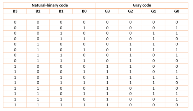
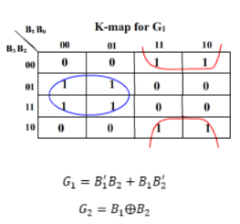
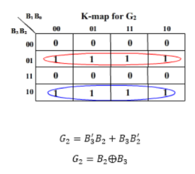
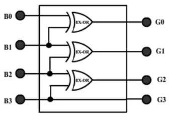
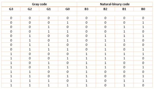
. Binary To Gray Code
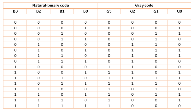
For this circuit, B3 B2 B1 B0 are inputs while G3 G2 G1 G0 are outputs.
K-map for the outputs:
And G3 = B3
2. Gray To Binary Code
Then the K-maps:
And B3 = G3
The realization of Gray-to-Binary converter is
Key Takeaways:
- These are the combinational circuits made by conversion of one code to another.
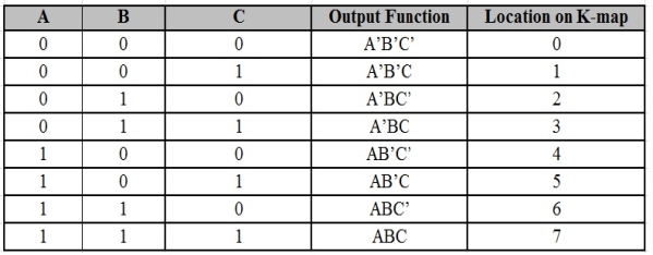
- It is a combinational circuit that converts binary information in the form of a 2N input lines into N output lines, which represent N bit code for the input.
- For simple encoders, only one input line is active at a time.
- For example: Octal to Binary encoder takes 8 input lines and generates 3 output lines.
8X3 Encoder
Truth Table –
D7 | D6 | D5 | D4 | D3 | D2 | D1 | D0 | X | Y | Z |
0 | 0 | 0 | 0 | 0 | 0 | 0 | 1 | 0 | 0 | 0 |
0 | 0 | 0 | 0 | 0 | 0 | 1 | 0 | 0 | 0 | 1 |
0 | 0 | 0 | 0 | 0 | 1 | 0 | 0 | 0 | 1 | 0 |
0 | 0 | 0 | 0 | 1 | 0 | 0 | 0 | 0 | 1 | 1 |
0 | 0 | 0 | 1 | 0 | 0 | 0 | 0 | 1 | 0 | 0 |
0 | 0 | 1 | 0 | 0 | 0 | 0 | 0 | 1 | 0 | 1 |
0 | 1 | 0 | 0 | 0 | 0 | 0 | 0 | 1 | 1 | 0 |
1 | 0 | 0 | 0 | 0 | 0 | 0 | 0 | 1 | 1 | 1 |
- From the above truth table it is seen that the output is 000 when D0 is active; 001 when D1 is active; 010 when D2 is active and so on.
Implementation –
- From the above truth table, the output Z is active when the input octal digit is 1, 3, 5 or 7.
- Y is active when input octal digit is 2, 3, 6 or 7 and X is active when input octal digits 4, 5, 6 or 7.
- Hence, the Boolean functions would be:
X = D4 + D5 + D6 + D7
Y = D2 +D3 + D6 + D7
Z = D1 + D3 + D5 + D7
- Hence, the encoder is realised with OR gates as follows:
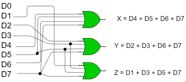
Fig: 12 8:3 encoder (ref.2)
- Limitation of the encoder is that only one input is active at a time.
- If more than one input are active, then the output of encoder is undefined.
- For example, if D6 and D3 are both active, then, our output would be 111 which is the output for D7.
- Problem arises when all inputs are 0.
- The encoder gives output 000 which actually is the output for D0. To avoid this, an extra bit is added to the output which is called the valid bit whose value is 0 when all inputs are 0 or 1.
Key Takeaways:
- It is a combinational circuit that converts binary information in the form of a 2N input lines into N output lines, which represent N bit code for the input.
- For simple encoders, only one input line is active at a time.
- It works as an inverse of an encoder.
- It is a combinational circuit which converts n input lines into 2n output lines.
- Taking an example of 3-to-8 line decoder.
Truth Table –
X | Y | Z | D0 | D1 | D2 | D3 | D4 | D5 | D6 | D7 |
0 | 0 | 0 | 1 | 0 | 0 | 0 | 0 | 0 | 0 | 0 |
0 | 0 | 1 | 0 | 1 | 0 | 0 | 0 | 0 | 0 | 0 |
0 | 1 | 0 | 0 | 0 | 1 | 0 | 0 | 0 | 0 | 0 |
0 | 1 | 1 | 0 | 0 | 0 | 1 | 0 | 0 | 0 | 0 |
1 | 0 | 0 | 0 | 0 | 0 | 0 | 1 | 0 | 0 | 0 |
1 | 0 | 1 | 0 | 0 | 0 | 0 | 0 | 1 | 0 | 0 |
1 | 1 | 0 | 0 | 0 | 0 | 0 | 0 | 0 | 1 | 0 |
1 | 1 | 1 | 0 | 0 | 0 | 0 | 0 | 0 | 0 | 1 |
Implementation
D0 is high when X = 0, Y = 0 and Z = 0. Hence,
D0 = X’ Y’ Z’
Similarly,
D1 = X’ Y’ Z
D2 = X’ Y Z’
D3 = X’ Y Z
D4 = X Y’ Z’
D5 = X Y’ Z
D6 = X Y Z’
D7 = X Y Z
Hence,

Decoder
Key Takeaways:
- It works as an inverse of an encoder.
- It is a combinational circuit which converts n input lines into 2n output lines.
- K-map method is a convenient method for minimization of Boolean functions up to 5 variables. But, it is very difficult to simplify more than 5 variables by using this method.
- Quine-McClukey is a tabular method based on the concept of prime implicants.
- Prime implicant is a product (or sum) term, which cannot be further reduced by combining with any other product (or sum) terms in the given Boolean function.
- This tabular method gets the prime implicants by repeatedly using the following Boolean identity.
Xy + xy’ = x(y + y’) = x.1 = x
Procedure of Quine-McCluskey Tabular Method
Steps for simplifying Boolean functions using Quine-McCluskey method:
Step 1 − Arranging the given min terms in ascending order and making groups based on the number of one’s present in the binary representations.
So, there are at most ‘n+1’ groups if there are ‘n’ Boolean variables or ‘n’ bits in the binary equivalent of min terms.
Step 2 − Comparing the min terms present in successive groups. If there is a change in only one-bit position, then taking the pair of two min terms. Placing the symbol ‘_’ in the differed bit position and keeping the remaining bits as it is.
Step 3 − Repeating step2 with newly formed terms till we get all required prime implicants.
Step 4 − Formulating the prime implicant table which consists of set of rows and columns. It can be placed row wise and min terms can be placed column wise. Put ‘1’ in the cells corresponding to the min terms that are covered in each prime implicant.
Step 5 – Now finding the essential prime implicants by observing each column. If the min term is covered by one prime implicant, then it is called as essential prime implicant. They will be a part of the simplified Boolean function.
Step 6 – The prime implicant table is reduced by removing the row and columns of each essential prime implicant corresponding to the min terms . This process is stopped when all min terms of given Boolean function are over.
Example
Simplify, f(W,X,Y,Z)=∑m(2,6,8,9,10,11,14,15) and f(W,X,Y,Z)=∑m(2,6,8,9,10,11,14,15)
Using Quine-McClukey tabular method.
Solution:
Group Name | Min terms | W | X | Y | Z |
GA1 | 2 | 0 | 0 | 1 | 0 |
8 | 1 | 0 | 0 | 0 | |
GA2 | 6 | 0 | 1 | 1 | 0 |
9 | 1 | 0 | 0 | 1 | |
10 | 1 | 0 | 1 | 0 | |
GA3 | 11 | 1 | 0 | 1 | 1 |
14 | 1 | 1 | 1 | 0 | |
GA4 | 15 | 1 | 1 | 1 | 1 |
Group Name | Min terms | W | X | Y | Z |
GB1 | 2,6 | 0 | - | 1 | 0 |
2,10 | - | 0 | 1 | 0 | |
8,9 | 1 | 0 | 0 | - | |
8,10 | 1 | 0 | - | 0 | |
GB2 | 6,14 | - | 1 | 1 | 0 |
9,11 | 1 | 0 | - | 1 | |
10,11 | 1 | 0 | 1 | - | |
10,14 | 1 | - | 1 | 0 | |
GB3 | 11,15 | 1 | - | 1 | 1 |
14,15 | 1 | 1 | 1 | - | |
|
|
|
|
|
|
Group Name | Min terms | W | X | Y | Z |
GB1 | 2,6,10,14 | - | - | 1 | 0 |
2,10,6,14 | - | - | 1 | 0 | |
8,9,10,11 | 1 | 0 | - | - | |
8,10,9,11 | 1 | 0 | - | - | |
GB2 | 10,11,14,15 | 1 | - | 1 | - |
10,14,11,15 | 1 | - | 1 | - | |
|
|
|
|
|
|
Group Name | Min terms | W | X | Y | Z |
GC1 | 2,6,10,14 | - | - | 1 | 0 |
| 8,9,10,11 | 1 | 0 | - | - |
GC2 | 10,11,14,15 | 1 | - | 1 | - |
Therefore, the prime implicants are YZ’, WX’ & WY.
The prime implicant table is shown below.
Min terms / Prime Implicants | 2 | 6 | 8 | 9 | 10 | 11 | 14 | 15 |
YZ’ | 1 | 1 |
|
| 1 |
| 1 |
|
WX’ |
|
| 1 | 1 | 1 | 1 |
|
|
WY |
|
|
|
| 1 | 1 | 1 | 1 |
The reduced prime implicant table is shown below.
Min terms / Prime Implicants | 8 | 9 | 11 | 15 |
WX’ | 1 | 1 | 1 |
|
WY |
|
| 1 | 1 |
Min terms / Prime Implicants | 15 |
WY | 1 |
Hence, f(W,X,Y,Z) = YZ’ + WX’ + WY.
Simplify
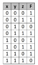
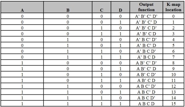
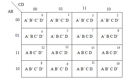
Y(A,B,C,D) =∑ m(0,1,3,7,8,9,11,15)
Groups are made with respect to the no. Of one’s present.
Now, comparing with the above table wherever we have a different bit present we put a ’-‘ there.
The same thing is done by comparing from the above table.
The table for prime implicants is:
Rounding the min terms which has X in column and hence the final answer is B’C’ + CD.
Reference
1. R. P. Jain, "Modern Digital Electronics", McGraw Hill Education, 2009.
2. M. M. Mano, "Digital logic and Computer design", Pearson Education India, 2016.
3. A. Kumar, "Fundamentals of Digital Circuits", Prentice Hall India, 2016.
Unit - 2
Combinational Digital Circuits
- It deals with binary numbers & variables.
- Therefore, also known as Binary Algebra or logical Algebra.
- A mathematician named as George Boole had developed this algebra in 1854.
- The variables that are used in this algebra are known as Boolean variables.
- Considering the range of voltages as logic ‘High’ is represented with ‘1’ and logic ‘Low’ is represented with ‘0’.
Boolean Postulates
- Considering the binary numbers 0 and 1, boolean variable (x) and its complement (x’).
- They known as literal.
- The possible logical OR operations are:
x + 0 = x
x + 1 = 1
x + x = x
x + x’ = 1
- Similarly, the possible logical AND operations are:
x.1 = x
x.0 = 0
x.x = x
x.x’ = 0
- These are the simple Boolean postulates and verification can be done by substituting the Boolean variable with ‘0’ or ‘1’.
K map
- Karnaugh map method or K-map method is the pictorial representation of the Boolean equations and Boolean manipulations are used to reduce the complexity in solving them. These can be considered as a special or extended version of the ‘Truth table’.
- Karnaugh map can be explained as “An array containing 2k cells in a grid like format, where k is the number of variables in the Boolean expression that is to be reduced or optimized”. As it is evaluated from the truth table method, each cell in the K-map will represent a single row of the truth table and a cell is represented by a square.
- The cells in the k-map are arranged in such a way that there are conjunctions, which differ in a single variable, are assigned in adjacent rows. The K-map method supports the elimination of potential race conditions and permits the rapid identification.
- By using Karnaugh map technique, we can reduce the Boolean expression containing any number of variables, such as 2-variable Boolean expression, 3-variable Boolean expression, 4-variable Boolean expression and even 7-variable Boolean expressions, which are complex to solve by using regular Boolean theorems and laws.
Minimization with Karnaugh Maps and advantages of K-map:
- K-maps are used to convert the truth table of a Boolean equation into minimized SOP form.
- Easy and simple basic rules for the simplification.
- The K-map method is faster and more efficient than other simplification techniques of Boolean algebra.
- All rows in the K-map are represented by using square shaped cells, in which each square in that will represent a minterms.
- It is easy to convert a truth table to k-map and k-map to Sum of Products form equation.
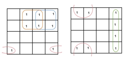
Grouping of K-map variables
- There are some rules to follow while we are grouping the variables in K-maps. They are
- The square that contains ‘1’ should be taken in simplifying, at least once.
- The square that contains ‘1’ can be considered as many times as the grouping is possible with it.
- Group shouldn’t include any zeros (0).
- A group should be the as large as possible.
- Groups can be horizontal or vertical. Grouping of variables in diagonal manner is not allowed.
- If the square containing ‘1’ has no possibility to be placed in a group, then it should be added to the final expression.
- Groups can overlap.
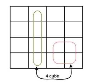
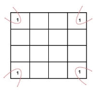
- The number of squares in a group must be equal to powers of 2, such as 1, 2, 4, 8 etc.
- Groups can wrap around. As the K-map is considered as spherical or folded, the squares at the corners (which are at the end of the column or row) should be considered as they adjacent squares.
- The grouping of K-map variables can be done in many ways, so they obtained simplified equation need not to be unique always.
- The Boolean equation must be in must be in canonical form, in order to draw a K-map.
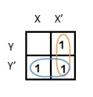
2 variable K-maps
There are 4 cells (22) in the 2-variable k-map. It will look like (see below image)
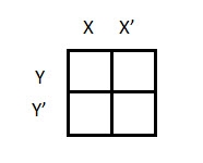
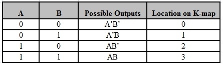
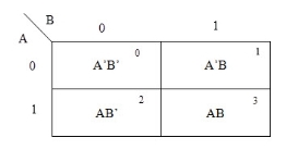
The possible min terms with 2 variables (A and B) are A.B, A.B’, A’. B and A’. B’. The conjunctions of the variables (A, B) and (A’, B) are represented in the cells of the top row and (A, B’) and (A’, B’) in cells of the bottom row. The following table shows the positions of all the possible outputs of 2-variable Boolean function on a K-map.
A general representation of a 2 variable K-map plot is shown below.
When we are simplifying a Boolean equation using Karnaugh map, we represent each cell of K-map containing the conjunction term with 1. After that, we group the adjacent cells with possible sizes as 2 or 4. In case of larger k-maps, we can group the variables in larger sizes like 8 or 16.
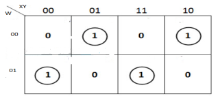
The groups of variables should be in rectangular shape that means the groups must be formed by combining adjacent cells either vertically or horizontally. Diagonal shaped or L-shaped groups are not allowed. The following example demonstrates a K-map simplification of a 2-variable Boolean equation.
Example
Simplify the given 2-variable Boolean equation by using K-map.
F = X Y’ + X’ Y + X’Y’
First, let’s construct the truth table for the given equation,
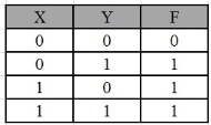
We put 1 at the output terms given in equation.
In this K-map, we can create 2 groups by following the rules for grouping, one is by combining (X’, Y) and (X’, Y’) terms and the other is by combining (X, Y’) and (X’, Y’) terms. Here the lower right cell is used in both groups.
After grouping the variables, the next step is determining the minimized expression.
By reducing each group, we obtain a conjunction of the minimized expression such as by taking out the common terms from two groups, i.e., X’ and Y’. So, the reduced equation will be X’ +Y’.
3 variable K-maps
For a 3-variable Boolean function, there is a possibility of 8 output min terms. The general representation of all the min terms using 3-variables is shown below.
A typical plot of a 3-variable K-map is shown below. It can be observed that the positions of columns 10 and 11 are interchanged so that there is only change in one variable across adjacent cells. This modification will allow in minimizing the logic.
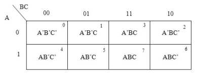
Up to 8 cells can be grouped in case of a 3-variable K-map with other possibilities being 1, 2 and 4.
Example
Simplify the given 3-variable Boolean equation by using k-map.
F = X’ Y Z + X’ Y’ Z + X Y Z’ + X’ Y’ Z’ + X Y Z + X Y’ Z’
First, let’s construct the truth table for the given equation,
We put 1 at the output terms given in equation.
There are 8 cells (23) in the 3-variable k-map. It will look like (see below image).
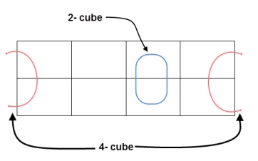
The largest group size will be 8 but we can also form the groups of size 4 and size 2, by possibility. In the 3 variable Karnaugh map, we consider the left most column of the k-map as the adjacent column of rightmost column. So, the size 4 group is formed as shown below.
And in both the terms, we have ‘Y’ in common. So, the group of size 4 is reduced as the conjunction Y. To consume every cell which has 1 in it, we group the rest of cells to form size 2 group, as shown below.
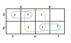
The 2-size group has no common variables, so they are written with their variables and its conjugates. So, the reduced equation will be X Z’ + Y’ + X’ Z. In this equation, no further minimization is possible.
4 variable K-maps
There are 16 possible min terms in case of a 4-variable Boolean function. The general representation of minterms using 4 variables is shown below.
A typical 4-variable K-map plot is shown below. It can be observed that both the columns and rows of 10 and 11 are interchanged.
The possible numbers of cells that can be grouped together are 1, 2, 4, 8 and 16.
Example
Simplify the given 4-variable Boolean equation by using k-map. F (W, X, Y, Z) = (1, 5, 12, 13)
Sol: F (W, X, Y, Z) = (1, 5, 12, 13)
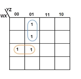
By preparing k-map, we can minimize the given Boolean equation as
F = W Y’ Z + W ‘Y’ Z
Key Takeaways:
- The range of voltages as logic ‘High’ is represented with ‘1’ and logic ‘Low’ is represented with ‘0’.
- Logical OR is summing of the literals and logical AND is multiplication of the two literals.
Simplifying K-maps:
- Selecting K-map on the basis of number of variables present in the Boolean function.
- If the Boolean function is in Max terms form, then place the zeroes at respective Max term cells in theK-map.
- If the Boolean function is in PoS form, then place the zeroes wherever required in K-map for which the given sum terms are valid.
- The maximum possibilities of grouping is checked for adjacent zeroes.
- It should be of powers of two.
- Starting from highest power of two and to the least power of two.
- Highest power is equivalent to the number of variables considered in K-map and least power is zero.
- Each group will give either a literal or one sum term.
- It is known as prime implicant.
- The prime implicant is an essential prime implicant when at least a single ‘0’ is not covered with any other groups but only that grouping covers.
- The simplified Boolean function contains all essential prime implicants and only the required prime implicants.
The process of simplifying the algebraic expression of a boolean function is called minimization. Minimization is important since it reduces the cost and complexity of the associated circuit.
For example, the function can be minimized. The circuits associated with above expressions is –
It is clear from the above image that the minimized version of the expression takes a less number of logic gates and also reduces the complexity of the circuit substantially.
Minimization is hence important to find the most economic equivalent representation of a Boolean function.
Minimization can be done using Algebraic Manipulation or K-Map method. Each method has it’s own merits and demerits.
- Karnaugh introduced a method for simplification of Boolean functions in an very easy way.
- This method is known as Karnaugh map method or K-map method.
- It is a graphical method, which comprises of 2n cells for ‘n’ variables.
- Here, the adjacent cells varies only in single bit position.
It is a special type of combinational circuit.
- It has n-data inputs, one output and m inputs select lines with 2m = n.
- It selects one of the n data inputs and routes it to the output.
- The selection of one of the inputs is done by the select lines.
- Depending on the code applied at the inputs, one of the n data sources is selected and transmitted to the single output Y.
- E is the enable input which is useful for cascading purpose.
- It is an active low terminal hence performs the required operation when it is low.

Fig. Block diagram of multiplexer
Multiplexers come in multiple variations
- 2: 1 multiplexer
- 4: 1 multiplexer
- 16: 1 multiplexer
- 32: 1 multiplexer
Block Diagram of 2:1 MUX
Truth Table of 2:1 MUX
Where x is don’t care.
Key Takeaways
- It has n-data inputs, one output and m inputs select lines with 2m = n.
- The selection of one of the inputs is done by the select lines.
DE- MULTIPLEXER
- It performs the inverse operation of a multiplexer as it receives one input and distributes it across its outputs.
- It has only one input and n outputs with m select input.
- At a time only one output line is selected by the select lines and that input is transmitted through the output line.
- It is equivalent to a single pole multiple way switch.
Various Demultiplexers are used as:
- 1: 2 demultiplexer
- 1: 4 demultiplexer
- 1: 16 demultiplexer
- 1: 32 demultiplexer
Block diagram
Truth Table
Where x is don’t care.
Key Takeaways:
- It performs the inverse operation of a multiplexer as it receives one input and distributes it across its outputs.
- It has only one input and n outputs with m select input.
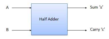
Half Adder
It is a combinational circuit which has two inputs and two outputs.
It is designed to add two single bit binary number A and B.
It has two outputs carry and sum.
Block diagram

Fig. Half adder
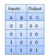
Truth Table
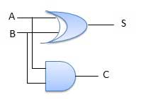
Circuit Diagram
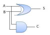
Fig. Half adder
Full Adder
- It is developed to overcome the drawback of Half Adder circuit.
- It can add two one-bit numbers A and B and a carry C.
- It is a three input and two output combinational circuit.
Block diagram

Fig. Full adder
Truth Table
Circuit Diagram
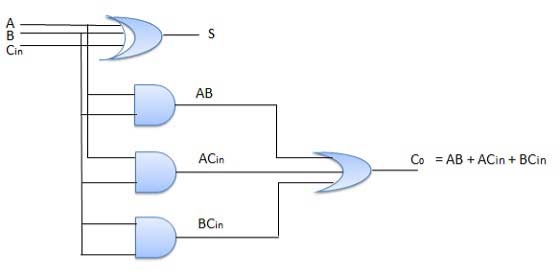
Fig. Full adder
Key Takeaways:
- Half adder is a combinational circuit which has two inputs and two outputs.
- Since there is no provision for carry in half adder, full adder is developed to overcome the drawback.
Subtractor
Half Subtractors
It is a combination circuit with two inputs and two outputs.
The difference between the two binary bits is obtained at the output and an output (Borrow) indicates if a 1 has been borrowed.
Here A is called as Minuend bit and B is called as Subtrahend bit.
Truth Table
Circuit Diagram

Fig. Half subtractor
Full Subtractors
It is a combinational circuit which has three inputs A,B,C and two output D and C'.
A is the 'minuend', B is 'subtrahend', C is the 'borrow' which is produced by the previous stage, difference output D and C' is the borrow output.
Truth Table
Circuit Diagram

Fig. Full subtractor
Key Takeaways:
- Half subtractor is a combinational circuit which has two inputs and two outputs.
- Since there is no provision for borrow in half subtractor, full subtractor is developed to overcome the drawback.
A decimal number contains 10 digits (0-9). Now the equivalent binary numbers can be found out of these 10 decimal numbers. In case of BCD the binary number formed by four binary digits, will be the equivalent code for the given decimal digits. In BCD we can use the binary number from 0000-1001 only, which are the decimal equivalent from 0-9 respectively.
Let, (12)10 be the decimal number whose equivalent Binary coded decimal will be 00010010. Four bits from L.S.B is binary equivalent of 2 and next four is the binary equivalent of 1.
BCD Addition
Example 1
Let, 0101 is added with 0110.
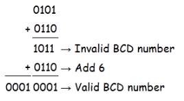
Check your self.
(0101)2 (5)10 and (0110)2 (6)10 (5)10 + (6)10 = (11)10
Example 2
Let 0001 0011 is added to 0010 0110.

 So no need to add 6 as because both are (0011)2 = (3)10 and (0111)2 = (7)10
Less than (9)10.
(0011)2 = (3)10 and (0111)2 = (7)10
This is the process of BCD Addition.
BCD Subtraction
Example: – 1
Let 0010 0001 0110 is subtracted from 0101 0100 0001.
- At first 1’s compliment of the subtrahend is done, which is 1101 1110 1001 and is added to 0101 0100 0001. This step is called adder 1.
- Now after addition if any carry occurs then it will be added to the next group of numbers towards MSB. Then EAC will be examined. Here, EAC = 1. So the result of addition is positive and true result of adder 1 will be transferred to adder 2.
- Now notice from LSB. There are three groups of four bit numbers. 1010 is added 1011 which is the first group of numbers because it do not have any carry. The result of the addition is the final answer.
- Carry 1 will be ignored as it is from the rule.
- Now move to the next group of numbers. 0000 is added to 0010 and gives the result 0010. It is the final result again.
- Now again move to the next group here 0000 is also added to 0011 to give the final result 0011.
- You may have noticed that in this two groups 0000 is added, because result of first adder do not contain any carry. Thus the results of the adder 2 is the final result of BCD Subtraction.

Therefore,
(0101 0100 0001) – (0010 0001 0110) = (0011 0010 0101)
Check.
(0101 0100 0001) = (541)10
(0010 0001 0110) = 21610
(0011 0010 0101) = 32510
We know that 541 − 216 = 325,
Thus we can say that our result of BCD Subtraction is correct.
- In this, for each adder block, the two bits that are to be added are available instantly.
- However, each of them waits for the carry to arrive from the previous one.
- So, it is impossible to generate the sum and carry of any block until the input carry is known.
- The block waits for the previous block to produce its carry. So there will be a considerable time delay which is known as carry propagation delay.
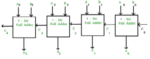
- Here, the sum is produced by the corresponding full adder as soon as the input signals are applied to it. The carry must propagate to all the stages so that output and carry settle their final steady-state value.
- The propagation time is equal to the propagation delay of each adder block, multiplied by the number of adder blocks in the circuit.
- It reduces the propagation delay by introducing more complex hardware.
- The ripple carry design is suitably transformed in such a way that the carry logic over fixed groups of bits is reduced to two-level logic.
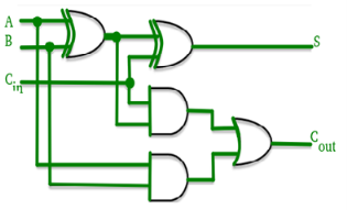
Fig. Look ahead Carry adder
Advantages and Disadvantages of Carry Look-Ahead Adder:
Advantages –
- The propagation delay is reduced.
- It provides the fastest addition logic.
Disadvantages –
- The circuit gets complicated as number of variables increase.
- It is costlier as it requires more hardware.
Key Takeaways:
- Here, the sum is produced by the corresponding full adder as soon as the input signals are applied to it. The carry must propagate to all the stages so that output and carry settle their final steady-state value.
- It reduces the propagation delay by introducing more complex hardware.
Serial binary adder is a combinational logic circuit that performs the addition of two binary numbers in serial form. Serial binary adder performs bit by bit addition. Two shift registers are used to store the binary numbers that are to be added.
A single full adder is used to add one pair of bits at a time along with the carry. The carry output from the full adder is applied to a D flip-flop. After that output is used as carry for next significant bits. The sum bit from the output of the full adder can be transferred into a third shift register.
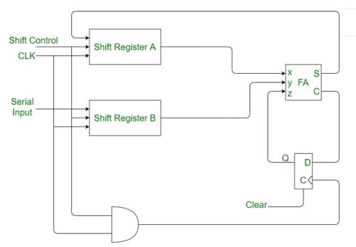
Fig: Block diagram of Serial Binary Adder
- An ALU performs mathematical and logical operations on binary numbers.
- They are located at the heart of every digital computer system and are one of the most important parts of a CPU (Central Processing Unit).
- Fetch-decode-execute refers to a computational process that continuously fetches the instructions from a memory, decodes them into operations and executes them to perform a calculation.
- These are simple steps which give rise to the complex behaviours that we expect from modern computing machines.

Fig. An illustration of the fetch-decode-execute cycle
This process can be further explained by linking each cycle step with three hardware subsystems called as a memory unit, a control unit, and an arithmetic unit.
MSI chips have less than 500 components or have more than 10 but less than 100 gates.
Although medium-scale integration has been replaced by other methods for the regular creation of microchips, recent news shows that engineers have been using carbon nanotube methods to develop new kinds of microchips on a medium-scale integration level.
- It performs comparison operation with more than four bits by cascading two or more 4-bit comparators.
- When two comparators are to be cascaded, the outputs of the lower-order comparator is connected to corresponding input of the higher-order comparator.
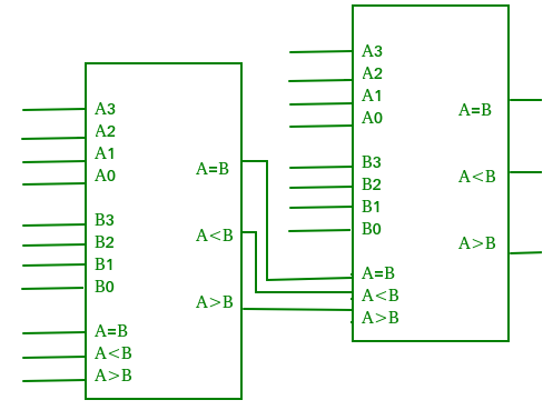
Fig. Digital comparator
Applications of Comparators –
- They are used in central processing units (CPUs) and microcontrollers (MCUs).
- They are used in control applications where the binary numbers represents physical variables such as temperature, position, etc. and are compared with a reference value.
- They are also used as process controllers and Servo motor controllers.
- They are used in password verification and biometric applications too.
- The parity generating technique is used as error detection technique for the data transmission.
- When binary data is transmitted and processed , it is subjected to noise and that noise can alter 0s to 1s and 1s to 0s of data bits in digital systems.
- Therefore, a parity generator is a combinational logic circuit that generates the parity bit at the transmitter end.
- The basic principle is that sum of odd number of 1s is always 1 and sum of even number of 1s is always zero.
- Such error detection and correction can be implemented by using Ex-OR gates.
Even Parity Generator
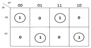
A 3-bit message is transmitted with an even parity bit. Hence assuming, the three inputs W,X and Y that are applied to the circuits and output bit is the parity bit P. The total number of 1s must be even, to generate the even parity bit P.
3- bit message | Even Parity | ||
W | X | Y | P |
0 | 0 | 0 | 0 |
0 | 0 | 1 | 1 |
0 | 1 | 0 | 1 |
0 | 1 | 1 | 0 |
1 | 0 | 0 | 1 |
1 | 0 | 1 | 0 |
1 | 1 | 0 | 0 |
1 | 1 | 1 | 1 |
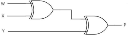
The K-map simplification for 3-bit message even parity generator is
From the above K-Map, the expression is:
P=W′X′Y+W′XY′+WX′Y′+WXY
P=W′(X′Y+XY′)+W(X′Y′+XY)
P=W′(X⊕Y)+W(X⊕Y)′=W⊕X⊕Y
Odd Parity Generator
Considering that the 3-bit data is transmitted with an odd parity bit. The three inputs are W, X and Y and P is the output parity bit. The total number of bits must be odd in order to generate the odd parity bit.
3- bit message | Odd Parity | ||
W | X | Y | P |
0 | 0 | 0 | 1 |
0 | 0 | 1 | 0 |
0 | 1 | 0 | 0 |
0 | 1 | 1 | 1 |
1 | 0 | 0 | 0 |
1 | 0 | 1 | 1 |
1 | 1 | 0 | 1 |
1 | 1 | 1 | 0 |
The K-map simplification for 3-bit message even parity generator is
Parity Checker
- They are of two types:
- Even parity checker: It checks error in the transmitted data, which contains message bits along with even parity.
- Odd parity checker: It checks error in the transmitted data, which contains message bits along with odd parity.
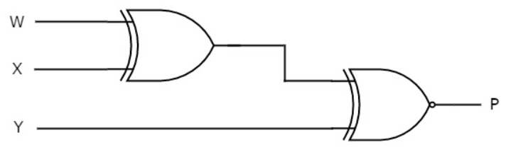
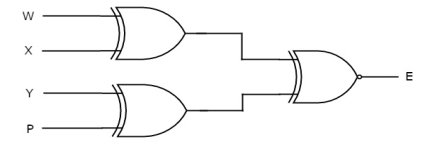
Even parity checker
Assume a 3-bit binary input, W, X and Y is transmitted along with an even parity bit, P. So, the resultant data contains 4 bits, that is received as the input of even parity checker.
It generates an even parity bit, E. This bit is zero, if the received data contains an even number of ones, which indicates that there is no error in the received data and vice versa.
The Truth table of an even parity checker is:
4-bit Received Data WXYP | Even Parity Check bit E |
0000 | 0 |
0001 | 1 |
0010 | 1 |
0011 | 0 |
0100 | 1 |
0101 | 0 |
0110 | 0 |
0111 | 1 |
1000 | 1 |
1001 | 0 |
1010 | 0 |
1011 | 1 |
1100 | 0 |
1101 | 1 |
1110 | 1 |
1111 | 0 |
The Boolean function of even parity check bit as
E = W xor X xor Y xor P
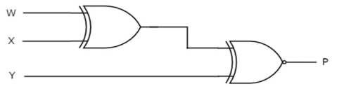
The following figure shows the circuit diagram of even parity checker.

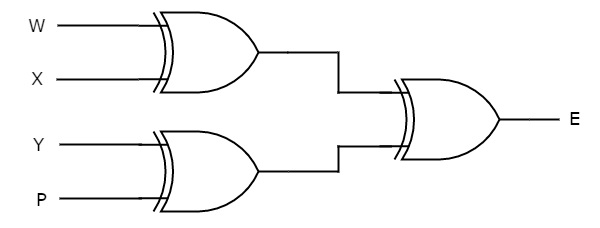
Odd Parity Checker
Assume a 3-bit binary input, W, X and Y is transmitted along with an odd parity bit, P. So, the resultant data contains 4 bits, that is received as the input of odd parity checker.
It generates an odd parity bit, E. This bit is zero, if the received data contains an odd number of ones, which indicates there is no error in the received data.
Key Takeaways:
- Even parity checker: It checks error in the transmitted data, which contains message bits along with even parity.
- Odd parity checker: It checks error in the transmitted data, which contains message bits along with odd parity.
- Even parity generator: It is generated in the transmitter end in message bits which contains even parity.
- Odd parity generator: It is generated in the transmitter end in message bits which contains odd parity.
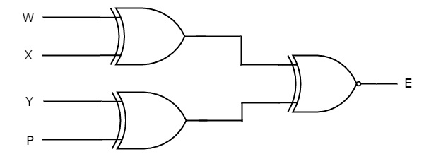
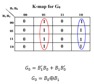
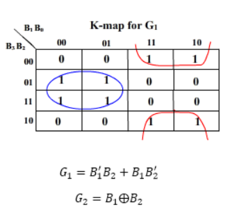
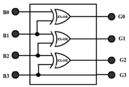
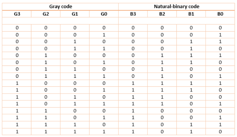
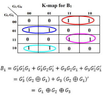
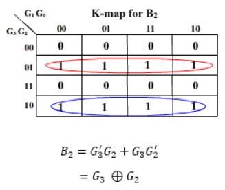
Binary To Gray Code
For this circuit, B3 B2 B1 B0 are inputs while G3 G2 G1 G0 are outputs.
K-map for the outputs:
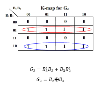
And G3 = B3
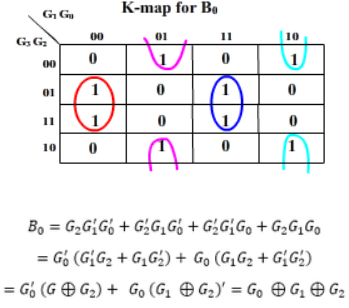
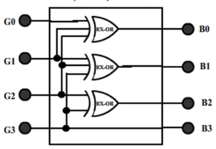
2. Gray To Binary Code
Then the K-maps:
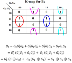
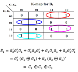
And B3 = G3
The realization of Gray-to-Binary converter is
Key Takeaways:
- These are the combinational circuits made by conversion of one code to another.
- It is a combinational circuit that converts binary information in the form of a 2N input lines into N output lines, which represent N bit code for the input.
- For simple encoders, only one input line is active at a time.
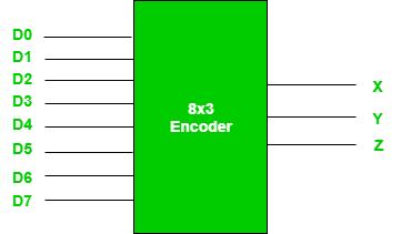
- For example: Octal to Binary encoder takes 8 input lines and generates 3 output lines.
Fig. 8X3 Encoder
Truth Table –
D7 | D6 | D5 | D4 | D3 | D2 | D1 | D0 | X | Y | Z |
0 | 0 | 0 | 0 | 0 | 0 | 0 | 1 | 0 | 0 | 0 |
0 | 0 | 0 | 0 | 0 | 0 | 1 | 0 | 0 | 0 | 1 |
0 | 0 | 0 | 0 | 0 | 1 | 0 | 0 | 0 | 1 | 0 |
0 | 0 | 0 | 0 | 1 | 0 | 0 | 0 | 0 | 1 | 1 |
0 | 0 | 0 | 1 | 0 | 0 | 0 | 0 | 1 | 0 | 0 |
0 | 0 | 1 | 0 | 0 | 0 | 0 | 0 | 1 | 0 | 1 |
0 | 1 | 0 | 0 | 0 | 0 | 0 | 0 | 1 | 1 | 0 |
1 | 0 | 0 | 0 | 0 | 0 | 0 | 0 | 1 | 1 | 1 |
- From the above truth table it is seen that the output is 000 when D0 is active; 001 when D1 is active; 010 when D2 is active and so on.
Implementation –
- From the above truth table, the output Z is active when the input octal digit is 1, 3, 5 or 7.
- Y is active when input octal digit is 2, 3, 6 or 7 and X is active when input octal digits 4, 5, 6 or 7.
- Hence, the Boolean functions would be:
X = D4 + D5 + D6 + D7
Y = D2 +D3 + D6 + D7
Z = D1 + D3 + D5 + D7
- Hence, the encoder is realised with OR gates as follows:
Fig: 8:3 encoder
- Limitation of the encoder is that only one input is active at a time.
- If more than one input are active, then the output of encoder is undefined.
- For example, if D6 and D3 are both active, then, our output would be 111 which is the output for D7.
- Problem arises when all inputs are 0.
- The encoder gives output 000 which actually is the output for D0. To avoid this, an extra bit is added to the output which is called the valid bit whose value is 0 when all inputs are 0 or 1.
Key Takeaways:
- It is a combinational circuit that converts binary information in the form of a 2N input lines into N output lines, which represent N bit code for the input.
- For simple encoders, only one input line is active at a time.
- It works as an inverse of an encoder.
- It is a combinational circuit which converts n input lines into 2n output lines.
- Taking an example of 3-to-8 line decoder.
Truth Table –
X | Y | Z | D0 | D1 | D2 | D3 | D4 | D5 | D6 | D7 |
0 | 0 | 0 | 1 | 0 | 0 | 0 | 0 | 0 | 0 | 0 |
0 | 0 | 1 | 0 | 1 | 0 | 0 | 0 | 0 | 0 | 0 |
0 | 1 | 0 | 0 | 0 | 1 | 0 | 0 | 0 | 0 | 0 |
0 | 1 | 1 | 0 | 0 | 0 | 1 | 0 | 0 | 0 | 0 |
1 | 0 | 0 | 0 | 0 | 0 | 0 | 1 | 0 | 0 | 0 |
1 | 0 | 1 | 0 | 0 | 0 | 0 | 0 | 1 | 0 | 0 |
1 | 1 | 0 | 0 | 0 | 0 | 0 | 0 | 0 | 1 | 0 |
1 | 1 | 1 | 0 | 0 | 0 | 0 | 0 | 0 | 0 | 1 |
Implementation
D0 is high when X = 0, Y = 0 and Z = 0. Hence,
D0 = X’ Y’ Z’
Similarly,
D1 = X’ Y’ Z
D2 = X’ Y Z’
D3 = X’ Y Z
D4 = X Y’ Z’
D5 = X Y’ Z
D6 = X Y Z’
D7 = X Y Z
Hence,
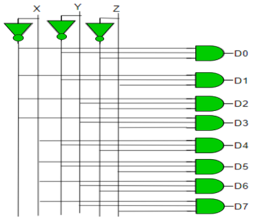
Fig. Decoder
Key Takeaways:
- It works as an inverse of an encoder.
- It is a combinational circuit which converts n input lines into 2n output lines.
- K-map method is a convenient method for minimization of Boolean functions up to 5 variables. But, it is very difficult to simplify more than 5 variables by using this method.
- Quine-McClukey is a tabular method based on the concept of prime implicants.
- Prime implicant is a product (or sum) term, which cannot be further reduced by combining with any other product (or sum) terms in the given Boolean function.
- This tabular method gets the prime implicants by repeatedly using the following Boolean identity.
Xy + xy’ = x(y + y’) = x.1 = x
Procedure of Quine-McCluskey Tabular Method
Steps for simplifying Boolean functions using Quine-McCluskey method:
Step 1 − Arranging the given min terms in ascending order and making groups based on the number of one’s present in the binary representations.
So, there are at most ‘n+1’ groups if there are ‘n’ Boolean variables or ‘n’ bits in the binary equivalent of min terms.
Step 2 − Comparing the min terms present in successive groups. If there is a change in only one-bit position, then taking the pair of two min terms. Placing the symbol ‘_’ in the differed bit position and keeping the remaining bits as it is.
Step 3 − Repeating step2 with newly formed terms till we get all required prime implicants.
Step 4 − Formulating the prime implicant table which consists of set of rows and columns. It can be placed row wise and min terms can be placed column wise. Put ‘1’ in the cells corresponding to the min terms that are covered in each prime implicant.
Step 5 – Now finding the essential prime implicants by observing each column. If the min term is covered by one prime implicant, then it is called as essential prime implicant. They will be a part of the simplified Boolean function.
Step 6 – The prime implicant table is reduced by removing the row and columns of each essential prime implicant corresponding to the min terms. This process is stopped when all min terms of given Boolean function are over.
Example
Simplify, f(W,X,Y,Z)=∑m(2,6,8,9,10,11,14,15)
And f(W,X,Y,Z)=∑m(2,6,8,9,10,11,14,15)
Using Quine-McClukey tabular method.
Solution:
Group Name | Min terms | W | X | Y | Z |
GA1 | 2 | 0 | 0 | 1 | 0 |
8 | 1 | 0 | 0 | 0 | |
GA2 | 6 | 0 | 1 | 1 | 0 |
9 | 1 | 0 | 0 | 1 | |
10 | 1 | 0 | 1 | 0 | |
GA3 | 11 | 1 | 0 | 1 | 1 |
14 | 1 | 1 | 1 | 0 | |
GA4 | 15 | 1 | 1 | 1 | 1 |
Group Name | Min terms | W | X | Y | Z |
GB1 | 2,6 | 0 | - | 1 | 0 |
2,10 | - | 0 | 1 | 0 | |
8,9 | 1 | 0 | 0 | - | |
8,10 | 1 | 0 | - | 0 | |
GB2 | 6,14 | - | 1 | 1 | 0 |
9,11 | 1 | 0 | - | 1 | |
10,11 | 1 | 0 | 1 | - | |
10,14 | 1 | - | 1 | 0 | |
GB3 | 11,15 | 1 | - | 1 | 1 |
14,15 | 1 | 1 | 1 | - | |
|
|
|
|
|
|
Group Name | Min terms | W | X | Y | Z |
GB1 | 2,6,10,14 | - | - | 1 | 0 |
2,10,6,14 | - | - | 1 | 0 | |
8,9,10,11 | 1 | 0 | - | - | |
8,10,9,11 | 1 | 0 | - | - | |
GB2 | 10,11,14,15 | 1 | - | 1 | - |
10,14,11,15 | 1 | - | 1 | - | |
|
|
|
|
|
|
Group Name | Min terms | W | X | Y | Z |
GC1 | 2,6,10,14 | - | - | 1 | 0 |
| 8,9,10,11 | 1 | 0 | - | - |
GC2 | 10,11,14,15 | 1 | - | 1 | - |
Therefore, the prime implicants are YZ’, WX’ & WY.
The prime implicant table is shown below.
Min terms / Prime Implicants | 2 | 6 | 8 | 9 | 10 | 11 | 14 | 15 |
YZ’ | 1 | 1 |
|
| 1 |
| 1 |
|
WX’ |
|
| 1 | 1 | 1 | 1 |
|
|
WY |
|
|
|
| 1 | 1 | 1 | 1 |
The reduced prime implicant table is shown below.
Min terms / Prime Implicants | 8 | 9 | 11 | 15 |
WX’ | 1 | 1 | 1 |
|
WY |
|
| 1 | 1 |
Min terms / Prime Implicants | 15 |
WY | 1 |
Hence, f(W,X,Y,Z) = YZ’ + WX’ + WY.
Simplify
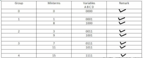
Y(A,B,C,D) =∑ m(0,1,3,7,8,9,11,15)
Groups are made with respect to the no. Of one’s present.
Group | Minterms | Variables A B C D | Remark |
0 | 0 | 0000 | ✔ |
|
|
|
|
1 | 1 | 0001 | ✔ |
| 8 | 1000 | ✔ |
|
|
|
|
2 | 3 | 0011 | ✔ |
| 9 | 1001 | ✔ |
|
|
|
|
3 | 7 | 0111 | ✔ |
| 11 | 1011 | ✔ |
|
|
|
|
4 | 15 | 1111 | ✔ |
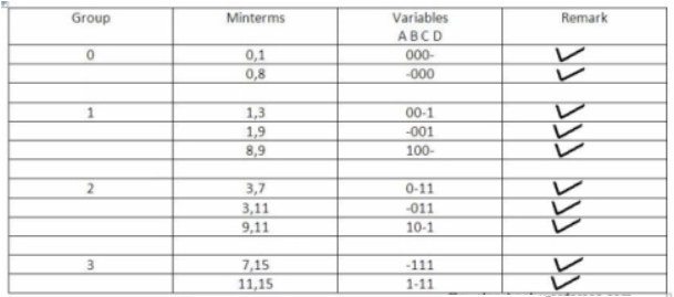
Now, comparing with the above table wherever we have a different bit present we put a ’-‘ there.
Group | Minterms | Variables A B C D | Remark |
0 | 0,1 | 000- | ✔ |
| 0,8 | -000 | ✔ |
|
|
|
|
1 | 1,3 | 00-1 | ✔ |
| 1,9 | -001 | ✔ |
| 8,9 | 100- | ✔ |
|
|
|
|
2 | 3,7 | 0-11 | ✔ |
| 3,11 | -011 | ✔ |
| 9,11 | 10-1 | ✔ |
|
|
|
|
3 | 7,15 | -111 | ✔ |
| 11,15 | 1-11 | ✔ |
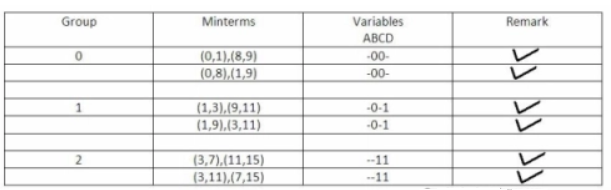
The same thing is done by comparing from the above table.
Group | Minterms | Variables A B C D | Remark |
0 | (0,1),(8,9) | -00- | ✔ |
| (0,8),(1,9) | -00- | ✔ |
|
|
|
|
1 | (1,3),(9,11) | -0-1 | ✔ |
| (1,9),(13,11) | -0-1 | ✔ |
|
|
|
|
2 | (3,7),(11,15) | --11 | ✔ |
| (3,11),(7,15) | --11 | ✔ |
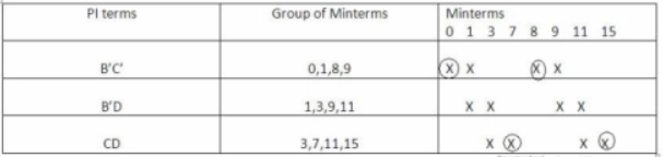
The table for prime implicants is:
PI terms | Group of Minterms | Minterms 0 1 3 7 8 9 11 15 |
B’C’ | 0,1,8,9 | Ⓧ × Ⓧ × |
B’D | 1,3,9,11 | × × × Ⓧ |
CD | 3,7,11,15 | × Ⓧ × Ⓧ |
Rounding the min terms which has X in column and hence the final answer is B’C’ + CD.
References:
1. R. P. Jain, "Modern Digital Electronics", McGraw Hill Education, 2009.
2. M. M. Mano, "Digital logic and Computer design", Pearson Education India, 2016.
3. A. Kumar, "Fundamentals of Digital Circuits", Prentice Hall India, 2016.
4. Thomas C Bartee, “Digital Computer Fundamentals”, McGraw Hill,1985.
5. Herbert Taub, Donald LSchilling “Digital Integrated Electronics”, McGraw Hill, 1977


