|
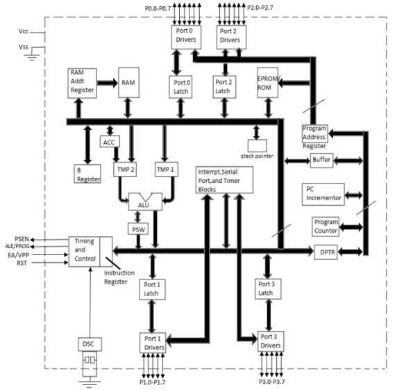
Figure 1. Internal Block Diagram
- 8051 microcontrollers were designed by Intel in 1981.
- It is an 8-bit microcontroller.
- It is built with 40 pins DIP (dual inline package), 4kb of ROM storage and 128 bytes of RAM storage, 2 16-bit timers.
- It consists of are four parallel 8-bit ports, which are programmable as well as addressable depending on the requirement.
- An on-chip crystal oscillator is integrated in the microcontroller having crystal frequency of 12 MHz.
- 8051 has 4 K Bytes of internal ROM. The address space is from 0000 to 0FFFh. If the program size is more than 4 K Bytes 8051 will fetch the code automatically from external memory.
- Accumulator is an 8 bit register widely used for all arithmetic and logical operations. Accumulator is also used to transfer data between external memory. B register is used along with Accumulator for multiplication and division. A and B registers together is also called MATH registers.
- PSW (Program Status Word). This is an 8 bit register which contains the arithmetic status of ALU and the bank select bits of register banks
Central Processor Unit (CPU)
CPU is the brain of any processing device of the microcontroller. It monitors and controls all operations that are performed on the Microcontroller units. It reads program written in ROM memory and executes them and does the expected task of that application
All arithmetic and logical functions are carried out by the ALU.
Addition, subtraction with carry, and multiplication come under arithmetic operations.
Logical AND, OR and exclusive OR (XOR) come under logical operations.
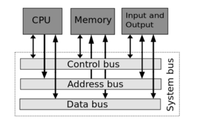
Basically, Bus is a collection of wires which work as a communication channel or medium for transfer of Data. There are three internal buses associated with processors: the data bus, address bus, and control bus. Together, these three make up the “system bus.”
|
Figure2. Internal System Bus
Control Bus:
Control signals move out of the processor, but not in to it.
Address and Data bus:
The data bus “width” of an MCU is typically 8-, 16-, 32- or 64-bits. The width of the data bus reflects the maximum amount of data that can be processed and delivered at one time. A 64-bit processor has a 64-bit data bus and can communicate 64-bits of data at a time, and whether the data is read or written is determined by the control bus.
The physical location of the data in memory is carried by the address bus. An internal hardware component, having received the address from the address bus and about to receive the data, enables a buffer to allow the flow of signals to or from the location that was designated by the address bus.
The address bus carries only the information regarding the address and is synchronized with the data bus to accomplish read/write tasks from the processor. The address bus is only as wide as is necessary to address all memory in the system.
|
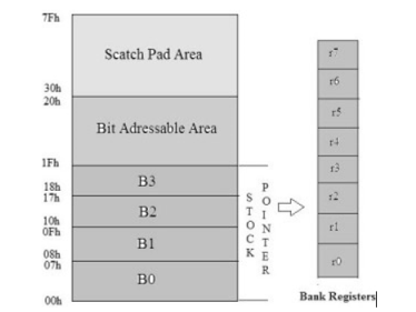
Figure 3. General Purpose Memory
The general-purpose memory is called as the RAM of the 8051 microcontrollers, which is divided into 3 areas such as banks, bit-addressable area, and scratch-pad area.
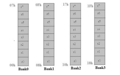
The banks contain different general-purpose registers such as R0-R7, and all such registers are byte-addressable registers that store or remove only 1-byte of data.
The B0, B1, B2, and B3 stand for banks, and each bank contains eight general-purpose registers ranging from ‘R0’ to ‘R7’. All these registers are byte-addressable. Data transfer between general-purpose registers to general-purpose registers is not possible. These banks are selected by the Program Status Word (PSW) register.
|
Figure 4. Bank Registers
SFRs related to the I/O ports: The 8051 has four I/O ports of 8 bits, for a total of 32 I/O lines. Whether a given I/O line is high or low and the value read from the line are controlled by the SFRs.
The SFRs control the operation or the configuration of some aspect of the 8051. For example, TCON controls the timers, SCON controls the serial port, the remaining SFRs, are auxiliary which means SFRs don't directly configure 8051. For example, once the serial port has been configured using SCON, the program may read or write to the serial port using the SBUF register.
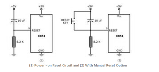
RESET is an active High input. When RESET is set to High, 8051 goes back to the power on state. The 8051 is reset by holding the RST high for at least two machine cycles and then returning it low.
There are two method of reset circuit:
1.Power On Reset.
- Initially charging of capacitor makes RST High
- When capacitor charges fully it blocks DC.
2.Manual Reset
- Closing the switch momentarily will make RST High.
|
Figure 5. Power and Reset Circuit
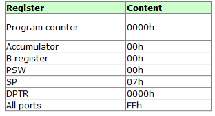
After a reset, the program counter is loaded with 0000H but the content of on-chip RAM is not affected.
OSCILLATOR CIRCUIT OF 8051 CONTROLLER
- The 8051 uses the crystal for precisely that to synchronize it’s operation. Effectively, the 8051 operates called as "machine cycles."
- A single machine cycle is the minimum amount of time in which a single 8051 instruction can be executed. although many instructions take multiple cycles.
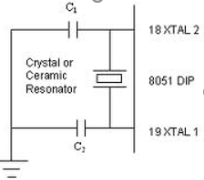
- 8051 has an on-chip oscillator. It needs an external crystal that decides the operating frequency of the 8051.
|
Figure6. Oscillator circuit
This can be achieved in two ways.
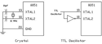
- The crystal is connected to pins 18 and 19 with stabilizing capacitors. 12 MHz (11.059MHz) crystal is often used and the capacitance ranges from 20pF to 40pF.
- The oscillator can also be a TTL clock source connected with a NOT gate as shown.
|
Figure7. Crystal Oscillator Circuit
Stack:
The register used to access the stack is called the SP (stack pointer) register. The stack pointer is 8 bits wide, which takes values of 00 to FFH.
When the 8051 is powered up, the SP register contains value 07. This means that RAM location 08 is the first location used for the stack by the 8051. The storing of a CPU register in the stack is called a PUSH, and pulling the contents off the stack back into a CPU register is called a POP.
Pushing onto the stack
In the 8051 the stack pointer (SP) points to the last used location of the stack. When we push data onto the stack, the stack pointer (SP) is incremented by one.
The SP is decremented when data is pushed onto the stack.
For example, when PUSH is executed, the contents of the register are saved on the stack and SP is incremented by 1.
For example, the instruction “PUSH 1″ pushes register Rl onto the stack.
MOV R6, #25H
MOV R1,#12H
MOV R4, #0F3H
PUSH 6
PUSH 1
PUSH 4
Solution:
| After PUSH 6 | After PUSH 1 | After PUSH 4 |
0B | 0B | 0B | 0B |
0A | 0A | 0A | 0A F3 |
09 | 09 | 09 12 | 09 12 |
08 | 08 25 | 08 25 | 08 25 |
Start SP=07 SP=08 SP=09 SP=0A
Popping the contents of the stack back into a given register is the opposite process of pushing. With every pop, the top byte of the stack is copied to the register specified by the instruction and the stack pointer is decremented once.
Example:
Examine the stack shows the contents of the registers and SP after execution of the following instructions.
POP 3 ; POP stack into R3
POP 5; POP stack into R5
POP 2; POP stack into R2
Solution:
| After PUSH 6 | After PUSH 1 | After PUSH 4 |
0B 54 | 0B | 0B | 0B |
0A F9 | 0A F9 | 0A | 0A |
09 76 | 09 76 | 09 76 | 09 |
08 6C | 08 6C | 08 6C | 08 6C |
Start SP=0B SP=0A SP=09 SP=08
Stack Pointer (SP)
SP or Stack Pointer points to the top of the Stack and it indicates the next data to be accessed. Stack Pointer can be accessed using PUSH, POP, CALL and RET Instructions. The Stack Pointer is an 8-bit register and upon reset, the Stack Pointer is initialized with 07H.
When writing a new data byte into the stack, the SP (Stack Pointer) is automatically incremented by 1 and the new data is written at an address SP+1. When reading data from stack, the data is retrieved from the Address in SP and after that the SP is decremented by 1 (SP-1)
A program counter is a 16-bit register that has no internal address. The program counter fetches the address of the next instruction to be executed from memory. The PC holds the address of next instruction residing in memory. When a command is encountered, it executes that instruction. PC increments and holds the address of the next instruction.
All 8051 microcontrollers have 4 I/O ports each comprising 8 bits which can be configured as inputs or outputs. Accordingly, in total of 32 input/output pins enabling the microcontroller to be connected to peripheral devices are available for use.
To configure a microcontroller pin as an input, it is necessary to apply a logic zero (0) to appropriate I/O port bit.
To configure a microcontroller pin as an input, it is necessary to apply a logic one (1) to appropriate port. In this case, voltage level on appropriate pin will be 5V (as is the case with any TTL input.
Port 0
|
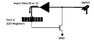
Figure 8. Input
If any pin of this port is configured as an input then it acts as if it “floats”. Such an input has unlimited input resistance and indetermined potential.
|
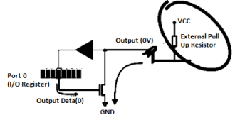
Figure 9. Output
When the pin is configured as an output, it acts as an “open drain”. By applying logic 0 to a port bit, the appropriate pin will be connected to ground (0V). To apply logic 1 (5V) on this output pin, it is necessary to build in an external pull-up resistor.
Port 1
P1 is a true I/O port, because it doesn't have any alternative functions as is the case with P0, but can be configured as general I/O only. It has a pull-up resistor built-in and is completely compatible with TTL circuits.
Port 2
P2 acts similarly to P0 when external memory is used. Pins of this port occupy addresses intended for external memory chip. This time it is about the higher address byte with addresses A8-A15. When no memory is added, this port can be used as a general input/output port showing features similar to P1.
Port 3
All port pins can be used as general I/O, but they also have an alternative function. To use these alternative functions, a logic one (1) must be applied to appropriate bit of the P3 register.
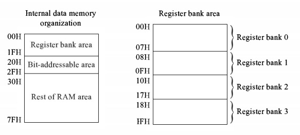
The internal data memory of 8051 is divided into two groups. These are a set of eight registers and a scratch pad memory. These eight registers are R0 toR7. The address range 00H to 07H is used to access the registers, and the rest are scratch pad memory.
Register Bank | |
00H to 07H | Register Bank 0 |
08H to 0FH | Register Bank 1 |
10H to 17H | Register Bank 2 |
18H to 1FH | Register Bank 3 |
|
Figure 10. Register Bank
So, the following addressing can be used to select register banks.
The concept of four register banks is very useful. For servicing the interrupts, this feature is good. The interrupt program can use one bank, and the interrupt Service Subroutine (ISS) can access another bank for better performance. As there are four banks, so for nested interrupts these can be used
Figure 11. Register Bank Selection
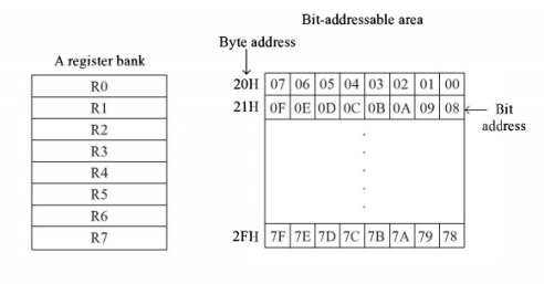
When all of the register banks are being used, the scratch pad area will be 20H to 7FH. But from 20H to 2FH (16 bytes or 128 bits) can be used as bit addressable RAM. Another section of bit addressable locations is 80H to FFH. The remaining locations (30H to 7EH) of the RAM can be used to store variable data and stack.
|
Figure 12. Bit Addressable area
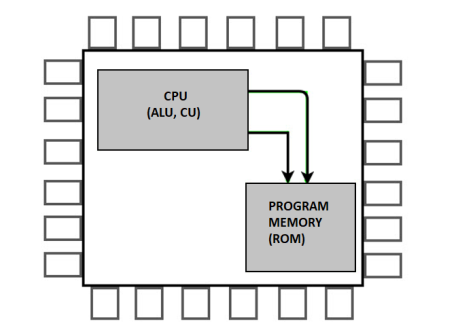
Program Memory (ROM) of 8051
|
Figure 13. Program Memory
In 4KB Internal ROM, the address space is 0000H to 0FFFH. If the program addresses exceed this value,CPU will automatically fetch the code from the external Program Memory.
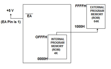
For External Access (EA Pin) must be pulled HIGH at this condition the CPU first fetches instructions from the Internal Program Memory in the address range of 0000H to 0FFFFH .If it exceeds the memory addresses limit, instructions are fetched from external ROM in address range of 1000H to FFFFH.
|
Figure14. External access
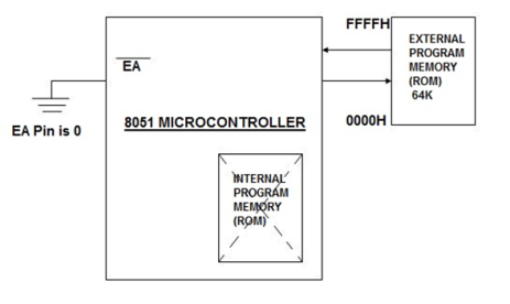
There is also an alternative method to fetch the instructions where the Internal ROM is ignored and instructions are fetched only from External Program Memory(External ROM).
For this purpose, EA pin must be connected to GND. The memory addresses of external ROM will be from 0000H to FFFFH.
|
Figure 15. External Program Memory
Data Memory (RAM)
- Data Memory or RAM stores temporary data and intermediate results generated during the normal operation of the microcontroller.
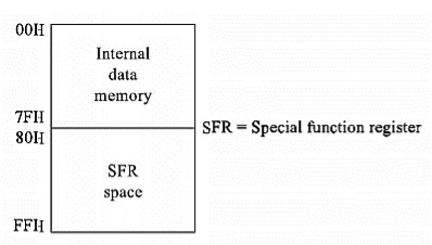
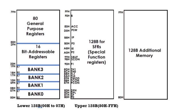
- Currently, 8051 Microcontroller has 256B of RAM. The first 128B memory addresses from 00H to 7FH is divided in to Working Registers. They are organized as Register Banks, Bit – Addressable Area and General Purpose RAM known as Scratchpad area.
- The first 128B of RAM (from 00H to 7FH), the first 32B of memory from addresses 00H to 1FH consists of 32 Working Registers organized into four banks with 8 Registers in each Bank.
|
Figure 16.Lower 128B(00H to 07H) Upper 128B(80H-FFH)
(Direct and Indirect Addressing) (Direct Addressing) (Indirect Addressing)
- The 4 banks are named as Bank0, Bank1, Bank2 and Bank3. Each Bank consists of 8 registers R0 – R7. Each Register can be addressed either by name or by address.
- To address the register by name, first the corresponding bank is selected. In order to select the bank, RS0 and RS1 bits of the Program Status Word (PSW) and Register (RS0 and RS1 are 3rd and 4th bits in the PSW Register) are used.
- When addressing these Register for example 12H the corresponding bank may or may not be selected. (12H corresponds to R2 in Bank2).
- The next 16B of the RAM that is from 20H to 2FH are Bit – Addressable memory locations. A total of 128 bits can be addressed individually using 00H to 7FH or an entire byte can be addressed as 20H to 2FH.
- The final 80B of the internal RAM addresses are from 30H to 7FH which is the general-purpose RAM area are byte addressable.
- These lower 128B of RAM can be addressed directly or indirectly.
- Instruction Fetch
- Instruction Decode
- Data Fetch/ Operand Fetch
- Instruction Execution
- Result Return.
Fetch:
- The CPU sends PC to Memory Address Register. The CPU activates tri-state buffer so MAR contents are placed on the address bus.
- CPU activates tri-state buffer so MAR contents are placed on the address bus.
- CPU sends read command on the control bus,R/W =1 and CE =1 to memory to indicate that it wants to read.
- In response to read command the memory returns the data stored in the memory location.
Decode Instruction
The decoding process allows the CPU to determine what instruction be performed so that CPU can tell how many operands it needs to fetch in order to perform the instruction. The opcode fetched from memory is decoded for next step to be moved into appropriate registers.
Execute the Instruction
If arithmetic or logic instruction is used utilize the ALU circuits to carry out the operation on data in registers. This is the only stage of the instruction cycle from the end user perspective.
Storing the Result
If destination is a memory address initiate memory write cycle to transfer the result from CPU to memory.
Key Takeaways:
The cycle starts immediately when power is applied to the system using initial PC value.
References:
- The 8051 Microcontroller and Embedded Systems using Assembly and C by Muhammad Ali Mazidi.
- The 8051 Microcontroller by I. Scott Mackenzie, Raphael C.W Phan
8051 Microcontrollers: Internals, Instructions, Programming, and Interfacing Book by Subrata Ghoshal
