4.1.1 Memory Interfacing
(i) External ROM Interfacing
|
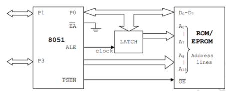
Figure 1. Interfacing of ROM/EPROM to μC 8051
The above figure shows how to interface ROM to 8051. Port 0 is used as multiplexed data and address lines. It gives lower order (A7-A0) 8-bit address in initial T cycle and higher order (A8-A150 as data bus.
The 8-bit address is latched using external latch and ALE signal from 8051. Port 2 provides higher order 9A15-A8) 8-bit address. PSEN is used to activate the output enable signal of external ROM/EPROM.
(ii) External RAM interfacing
|
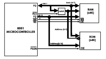
Figure 2. Interfacing of RAM with μC 8051
The above figure shows how to connect or interface external RAM(data memory) to 8051. Port 0 is used as multiplexed data & address lines. Address lines are decoded using external latch & ALE signal from 8051 to provide lower order (A7-A0) address lines. Port 2 gives higher order address lines. RD & WR signals from 8051 selects the memory read & memory write operations, respectively.
(iii) I/O expansion buses
|
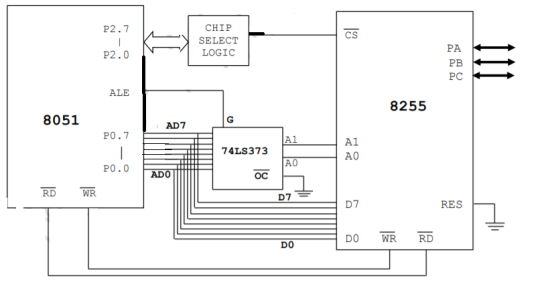
Figure 3. 8051 CONNECTION TO THE 8255.
For external memory interfacing to 8051 port 0 & port 2 are used as multiplexed address/data bus & higher order data bus respectively.
If circuit needs on-chip peripherals e.g. serial I/O & interrupts then only port is available for I/On such situation, I/O expansions is necessary & it is achieved by using 8255. data bus of 8255 is connected to the port 0. address line A0 & A1, after latches are connected to A0 & A1 of the 8255.
For external memory interfacing to 8051 port 0 & port 2 are used as multiplexed address/data bus & higher order data bus respectively.
If the circuit needs on-chip peripherals then only port is available for I/O. In such situation I/O expansions is achieved by 8255. The address line Ao and A1 are connected to 8255 Ao A1.
4.1.2 Control signals
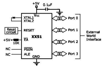
There are 3 control signals, EA,PSEN and ALE. These signals known as External Access (EA), Program Store Enable (PSEN), and Address Latch Enable (ALE) are used for external memory interfacing.
|
Figure 4. Inputs for Operation
The control signals are used for external memory interfacing. If there is no requirement of external memory interfacing then, EA pin is pulled high and two others PSEN and ALE are left alone.
4.1.3 Memory Wait States
The wait state is an extra bus clock cycle that is added to the memory access to allow time for the information to be extracted and appear on the processor bus. This addition of wait states limits the processing speed to less than 60MIPS
Key Take Aways:
8051 external program memory interface with the upper address on Port 2, the lower address and data in/out multiplexed on Port 0, and the ALE and PSEN strobes.
4.2.1 Interfacing of ADC
ADC0808/0809:
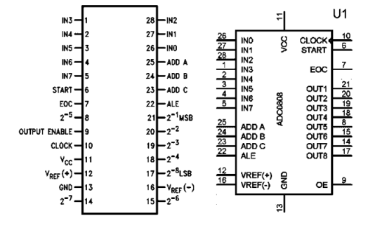
ADC0808/0809 is a monolithic CMOS device which has 28 pin and gives 8-bit value in output and 8- channel ADC input pins (IN0-IN7). I
It has resolution of 8 so it can encode the analoge data into one of the 256 levels (28).
This device has three channel address line namely: ADDA, ADDB and ADDC for selecting channel.
Pin Diagram for ADC0808
|
Figure 5. ADC 0808 Pin
ADC0808/0809 requires a clock pulse for conversion. This can be provided by using oscillator or by using microcontroller.
Select the input channel using address lines, like the input line IN0 by keeping all three address lines (ADDA, ADDB,ADDC) low.
Suppose IN2 is selected the keep ADDA and ADDB low and ADDC high.
ADC Channel name | ADDC Pin | ADDB Pin | ADDA Pin |
IN0 | Low | Low | Low |
IN1 | Low | Low | High |
IN2 | Low | High | Low |
IN3 | Low | High | High |
IN4 | High | Low | Low |
IN5 | High | Low | High |
IN6 | High | High | Low |
IN7 | High | High | High |
SOC [Start of conversion]:
When High to low signal is appears to this pin of ADC, ADC then starts conversion
|
Figure 6. SOC
EOC [End of conversion]:
ADC sends this high EOC signal to Micro-Controller to indicate completion of conversion.
OE [Output Enable]:
When a high signal is applied to this pin, the output latch of ADC gets enabled and the converted data is made available to Micro-Controller.
The reference voltage determines the range of analog input voltage.
For example: - If reference voltage is 5V then analog voltage range is from 0V-5V. If the reference voltage is 2.56V then the Analog signal range is from 0V-2.56V.
The frequency of clock signal applied determines the conversion speed.
Working:
- First the microcontroller provides a 500 KHz clock signal to ADC0808 because the Timer 0 interrupt as ADC requires clock signal to operate.
- Then the microcontroller sends a LOW to HIGH level signal to ALE pin (active-high pin) of ADC0808 to enable the latch in the address.
- By applying HIGH to LOW Level signal to SC (Start Conversion), ADC starts analog to digital conversion. And then wait for the EOC (End of Conversion) pin to go LOW.
- When EOC goes LOW, it means analog to digital conversion has been completed and data is ready to use.
- After this, microcontroller enables the output line by applying a HIGH to LOW signal to OE pin of ADC0808.
- ADC0808 gives ratio metric conversion output at its output pins.
Radiometric conversion is given by
Vin/(Vfs – Vz) = Dx / (Dmax – Dmin)
Where:
Vin is input voltage for conversion
Vfs is full scale voltage
Vz is zero voltage
Dx is data point being measured
Dmax is maximum data limit
Dmin is minimum data limit.
Interfacing Diagram:
|
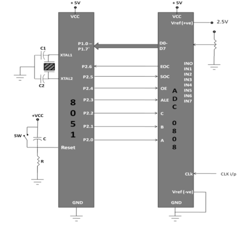
Figure 7. Interfacing 8051 with ADC0808
Program:
SOC EQU P2.6
EOC EQU P2.5
OE EQU P2.4
ALE EQU P2.3
ADDR_C EQU P2.2
ADDR_B EQU P2.1
ADDR_A EQU P2.0ORG 0000H
MOV P1, #0FFH
SETB P2.5
CLR SOC
CLR OE
CLR ALE
AGAIN: CLR ADDR_C
CLR ADDR_B
CLR ADDR_A
SETB SOC
SET ALE
ACALL DELAY
CLR SOC
CLR ALE
BACK: JB EOC BACK
HERE: JNB EOC HERE
SETB OE
MOV A,P1
ACALL CONVERSION
ACALL DISPLAY
AGAIN: SJMP AGAIN
Key Take Aways:
Telephone modem is one of the examples of ADC, which is used for internet, it converts analog data into digital data.
4.2.2 Interfacing of DAC
DAC (0808)
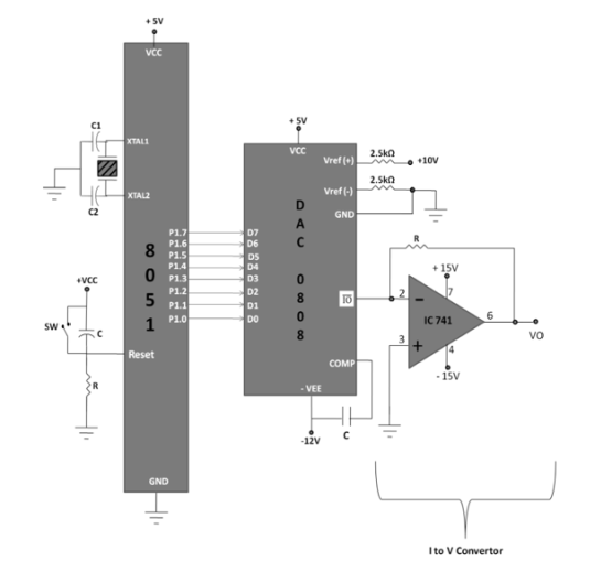
In these systems microcontroller generates output, which is in digital form, but the controlling system requires analog signal as they don't accept digital data. There is a need to use DAC which converts digital data into equivalent analog voltage.
- In the figure shown, we use 8-bit DAC 0808. This IC converts digital data into equivalent analog current. Hence, we require an I to V converter to convert this current into equivalent voltage.
According to theory of DAC Equivalent analog output is given as:
Vo = Vref[ Do/2 + D1/4 + D2/8 + D3/16+D4/32 +D5/64+D6/128+D7/256]
Ex:
1. IF data =00H [00000000] and
Vref = 10V
Vo = 10[ 0/2+0/4+0/8+0/16+0/32+0/64+0/128+0/256]
Therefore, V0= 0 Volts.
2. If data is 80H [10000000],
and Vref = 10V
Vo = 10[ ½ +0/4+0/8+0/16+0/32+0/64+0/128+0/256]
Therefore, V0= 5 Volts.
Different Analog output voltages for different Digital signal is given as:
DATA | OUTPUT VOLTAGE |
00H | 0V |
80H | 5V |
FFH | 10V |
|
Figure 8. Interfacing 8051 with DAC 0808
Program:
ORG 000H
MOV P1, #00H
call squarwave
call triwave
call stairwave
jmp repeat
squarwave: MOV P1,#FFH
call delay2sec
MOV P1,#00H
call delay2sec
ret
triwave: MOV R7,#00H
triwave1: MOV P1,R7
inc R7
cjne R7, #FFH, triwave1
MOV R7, #FFh
Triwave2: MOV P1, R7
djnz R7, triwave2
RET
Stairwave: MOV P1, #00H
call delay2sec
MOV P1, #20H
Call delay2sec
MOV P1, #40H
Call delay2sec
RET
delay1sec: MOV R0,#10
del2 : MOV R1,#250
del1: MOV R2,#250
DJNZ R2,$
DJNZ R1,del2
DJNZ R0,del1
RET
Delay2sec: MOV R0,#20
del2 : MOV R1,#250
del1: MOV R2,#250
DJNZ R2,$
DJNZ R1,del21
DJNZ R0,del22
RET
END
Key Take Aways:
The Digital to Analog converter (DAC) is a device, that is widely used for converting digital pulses to analog signals.
4.2.3 Timers
The 8051 has two timers: timer0 and timer1. They can be used either as timers or as counters. Both timers are 16 bits wide. Since the 8051 is an 8-bit architecture, each 16-bit is accessed as two separate registers of low byte and high byte.
Timer0 registers is a 16- bit register and accessed as low byte and high byte. The low byte is referred as a TL0 and the high byte is referred as TH0. These registers can be accessed like any other registers.
|
Figure 9.Timer0
Timer1 registers is also 16- bits register and is split into two bytes, referred to as TL1 and TH1.
|
Figure 10.Timer 1
TMOD (timer mode) Register:
This is an 8-bit register which is used by both timers 0 and 1 to set the various timer modes. In this TMOD register, lower 4 bits are set aside for timer0 and the upper 4 bits are set aside for timer1.
In each case, the lower 2 bits are used to set the timer mode and upper 2 bits to specify the operation.
|
Figure.11TMOD Register
- The first bit is a GATE bit. Every timer has a means of start and stop. Some timers are done by software, some by hardware, and some by both software and hardware controls.
- In the hardware way of starting and stopping the timer is by an external source is achieved by making GATE=1 in the TMOD register. And if we change to GATE=0 then no external hardware to start and stop the timers.
- The second bit is C/T bit which is used to decide whether the timer is used as time delay generator or event counter. If this bit is 0 it is used as a timer and if it is 1 then it is used as counter.
- In upper or lower 4 bits, the last bits third and fourth are known as M1 and M0 respectively. These are used to select the timer mode.
M0 | M1 | Mode | Operating Mode |
0 | 0 | 0 | 13-bit timer mode. 8 bit timer/counter THx and TLx as –bit prescalar |
0 | 1 | 1 | 16-bit timer mode , 16-bit timers/counters THx and TLx as 5-bit prescalar |
1 | 0 | 2 | 8-bit auto reload mode, 8-bit auto reload timer/counter; THx holds a value which is to be reloaded into TLx each time it overflows |
1 | 1 | 3 | Split timer mode |
Mode 1-
- It is a 16-bit timer which allows values from 0000 to FFFFH to be loaded into the timer’s registers TL and TH.
- After TH and TL are loaded with a 16-bit initial value, the timer must be started.
- This is done t by “SETB TR0” for timer 0 and “SETB TR1” for timer 1.
- After the timer is started. It starts count up until it reaches its limit of FFFFH.
- When it rolls over from FFFF to 0000H, it sets high a flag bit called TF (timer flag).
- This timer flag can be monitored. When this timer flag is raised, one option would be stop the timer with the instructions “CLR TR0“ or CLR TR1 for timer 0 and timer 1 respectively.
- Note that timer flag is TF0 for timer 0 and TF1 for timer1. After the timer reaches its limit and rolls over, in order to repeat the process the registers TH and TL must be reloaded with the original value and TF must be reset to 0.
Mode0-
- Mode 0 is a 13-bit timer instead of 16-bit.
- The 13-bit counter hold values between 0000 to 1FFFH in TH-TL. Therefore, when the timer reaches its maximum of 1FFH, it rolls over to 0000, and TF is raised.
Mode 2-
- It is an 8bit timer which allows values from 00 to FFH to be loaded into the timer’s register TH.
- After TH is loaded with 8bit value, the 8051 gives a copy of it to TL. Then the timer is started which is done by the instruction “SETB TR0” for timer 0 and “SETB TR1” for timer1.
- After timer is started, it starts to count by incrementing the TL register. until it reaches its limit of FFH.
- When it rolls over from FFH to 00. It sets high the TF (timer flag). If we are using timer 0, TF0 goes high. If TF1 is used then TF1 is raised.
- When Tl register rolls from FFH to 00 and TF is set to 1, TL is reloaded automatically with the original value and kept in TH register. To repeat the process clear TF. This makes mode 2 auto reload, in contrast in mode 1 in which programmer has to reload TH and TL.
Mode3-
Mode 3 is also known as a split timer mode. Timer 0 and 1 may be programmed to be in mode 0, 1 and 2 independently.Timers do not operate independently if mode 3 is chosen for timer 0. Placing timer 1 in mode 3 causes it to stop counting; the control bit TR1 and the timer 1 flag TF1 are then used by timer0.
TCON Register
Bits and symbol and functions of every bits of TCON are as follows:
TF1 | TR1 | TF0 | TR0 | IE1 | IT1 | IE0 | IT0 |
Figure .TCON Register
Bit | Symbol | Functions |
7 | TF1 | Timer1 overflow flag. Set when timer rolls from all 1’s to 0 |
6 | TR1 | Timer 1 run control bit. Set to 1 by programmer to enable timer to count. |
5 | TF0 | Timer 0 overflow flag |
4 | TR0 | Timer 0 run control bit |
3 | IE1 | External Interrupt 1 edge flag |
2 | IT1 | External Interrupt 1 signal type control bit |
1 | IE0 | External Interrupt 0 edge flag |
0 | IT0 | External Interrupt 0 signal type control bit |
4.2.4 Counters
- In the counter mode, the external events are counted. In this mode, the timer register is incremented for each 1 to 0 transition of the external input pin. This type of transitions is treated as events. To determine the 1or 0 transitions, another machine cycle will be needed. So, in this mode, at least two machine cycles are needed.
- There are four different modes of the Timer or Counter. The Mode 0 to Mode 2 are for both of the Timer/Counter. Mode 3 has a different meaning for each timer register. There is a register called TMOD. This register can be programmed to configure these timers or counters.
TMOD(Timer Mode) is an SFR. The address of this register is 89H. This is not bit-addressable.
Timer | Timer1 Mode | Timer0 Mode | ||||||
Bit Details | Gate (G) | C/T | M1 | M0 | Gate (G) | C/T | M1 | M0 |
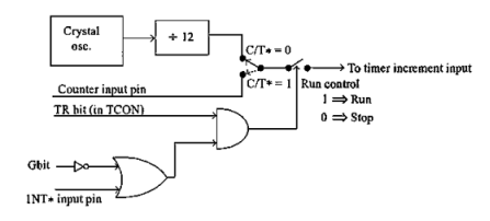
The circuit that controls the running of the timers is shown in the figure.
|
Figure 12. Timers
Bit Details | High Value(1) | Low Value(0) |
C/T | Configure for the Counter operations | Configure for the Timer operations |
Gate (G) | Timer0 or Timer1 will be in RunMode when TRX bit of TCON register is high. | Timer0 or Timer1 will be in RunMode when TRX bit of TCON register is high and INT0 or INT1 is high. |
Bit Details | 00 | 01 | 10 | 11 |
M1 M0 | This is for Mode 0. (8-bit timer/counter, with 5-bit pre-scaler) | This is Mode 1. (16-bit timer/counter) | This is Mode 3 (8-bit auto reload-timer/counter) | This is Mode 3 (The function depends on Timer0 or Timer1) |
The Gate bit will be high when the timer or counter is in mode 0 to 2.
To configure Timer0 as 16-bit event counter and Timer1 as 8-bit auto reload counter, use the bit pattern as 0 0 1 0 0 1 0 1. It is equivalent to 25H. Then if we want to program the TMOD register with this bit pattern, we can use this instruction:
MOVTMOD,#25H
The above instruction is executed, then the timer/counter will be controlled by the software. To configure the system as hardware controlled mode, then the gate bits will be 1. The bit patterns will be 1 0 1 0 1 1 0 1 = ADH
Then use this instruction:
MOV TMOD, #0ADH
The Mode 0 operation is the 8-bit timer or counter with a 5-bit pre-scaler. It is a 13-bit timer/counter. It uses 5 bits of TL0 or TL1 and all of the 8-bits of TH0 or TH1.
|
Figure13. Timer selection
In this example the Timer1is selected, every 32 (25)event for counter operations or 32 machine cycles for timer operation, the TH1 register will be incremented by 1. When the TH1overflows from FFH to 00H, then the TF1 of TCON register will be high, and it stops the timer/counter.
Example, we can say that if the TH1 is holding F0H, and it is in timer mode, then T
F1will be high after 10H * 32 = 512 machine cycles.
MOVTMOD,#00H
MOV TH1,#0F0H
MOV IE,#88H
SETB TR1
In the above program, the Timer1 is configured as timer mode 0. In this case Gate = 0. Then the TH1 will be loaded with F0H, then enable the Timer1 interrupt. At last set the TR1 of TCON register, and start the timer.
The Mode 1 operation is the 16-bit timer or counter. In the following diagram, we are using Mode 1 for Timer0.
|
Figure 14. Timer Operation
In this case every event for counter operations or machine cycles for timer operation, the TH0– TL0 register-pair will be incremented by 1. When the register pair overflows from FFFFH to 0000H, then the TF0 of TCON register will be high, and it stops the timer/counter.
Example, we can say that if the TH0 – TL0 register pair is holding FFF0H, and it is in timer mode, then TF0 will be high after 10H = 16 machine cycles. When the clock frequency is 12MHz, then the following instructions generate an interrupt 16 µs after Timer0 starts running.
MOV TMOD,#01H
MOV TLO,#F0H
MOV TH0, #0FFH
MOV IE,#82H
SETB TR0
In the above program, the Timer0 is configured as timer mode 1. In this case Gate = 0. Then the TL0 will be loaded with F0H and TH0 is loaded with FFH, then enable the Timer0 interrupt. At last set the TR0 of TCON register, and start the timer.
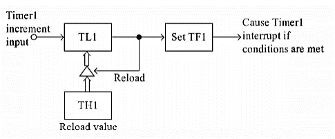
The Mode 2 operation is the 8-bit auto reload timer or counter. In the following diagram, we are using Mode 2 for Timer1.
|
Figure 15. Mode 2
In this case every event for counter operations or machine cycles for timer operation, the TL1register will be incremented by 1. When the register pair overflows from FFH to 00H, then the TF1 of TCON register will be high, also theTL1 will be reloaded with the content of TH1 and starts the operation again.
Example, If the TH1 and TL1 register both are holding F0H and it is in timer mode, then TF1 will be high after 10H= 16 machine cycles. When the clock frequency is 12MHz this happens after 16 µs, then the following instructions generate an interrupt once every 16 µs after Timer1 starts running
MOV TMOD,#20H
MOV TL1,#0F0H
MOV TH1,#0F0H
MOV #88H
SETBTR1
In the above program, the Timer1 is configured as timer mode 2. In this case Gate = 0. Then the TL1 and TH1 are loaded with F0H. then enable the Timer1 interrupt. At last set the TR1 of TCON register, and start the timer.
Timer1 in mode 2 generates the desired baud rate when the serial port is working on Mode 1 or 3.
Key Take Aways:
The 8051 has two counters/timers which can be used either as timer to generate a time delay or as counter to count events.
4.2.5 Memory Devices
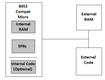
The memory types are: On-Chip Memory, External Code Memory, and External RAM. On-Chip Memory refers to any memory (Code, RAM, or other) that physically exists on the microcontroller itself. External Code Memory is code (or program) memory that resides off-chip. This is often in the form of an external EPROM. External RAM is RAM memory that resides off-chip. This is often in the form of standard static RAM or flash RAM.
|
Figure16. Memory Types
Key Take Aways:
The architecture 8051 consists of internal RAM, special function registers, program memory, and external data memory.
References:
- The 8051 Microcontroller and Embedded Systems using Assembly and C by Muhammad Ali Mazidi.
- The 8051 Microcontroller by I. Scott Mackenzie, Raphael C.W Phan
8051 Microcontrollers: Internals, Instructions, Programming, and Interfacing Book by Subrata Ghoshal
