Module 3
Sampling Theorem
“Converting the analog or continuous time signal into equivalent discrete form is known as Sampling.”
Taking piece of data from whole data is known as a Sample and that data is continuous in the time domain.
Converting the analog signal generated by source into digital i.e. in 0s and 1s form is known as discretization. This discretization of analog signal is known as Sampling.
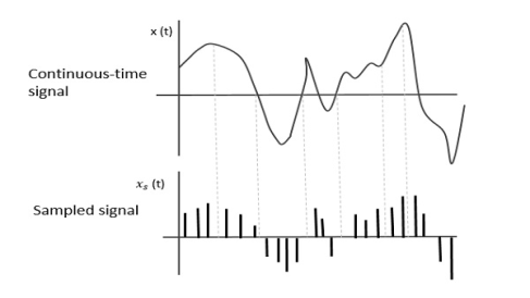
Signal x (t) and a sampled signal xs (t) are the continuous-time signals shown in figure below. When periodic impulse train is multiplied with x (t) is multiplied, the sampled signal xs (t) is obtained.
Sampling Rate
To make the signal discrete, the gap between the samples should be fixed. A sampling period Ts is the gap between samples.
Sampling Frequency = 1Ts = fs
Where,
Ts: the sampling time.
Fs: the sampling frequency or the sampling rate.
Sampling frequency is the inverse/reciprocal of the sampling period. This sampling frequency is nothing but Sampling rate. The number of samples taken per second is called as sampling rate.
To reconstruct the analog signal from the digitized signal, the sampling rate should be highly considered. The rate of sampling should be fixed so that the data in the message signal should neither be lost nor it should get over-lapped. And that fixed rate is called as Nyquist rate.
Nyquist Rate
Suppose that a signal is band-limited with no frequency element higher than W Hz. That means, W = highest frequency. For effective reproduction of the original signal, the sampling rate should be double the highest frequency.
Which means,
fS=2W
Where,
FS: sampling rate
W: highest frequency
This rate of sampling is known as Nyquist rate.
A theorem called, Sampling Theorem, was stated on the theory of this Nyquist rate.
Sampling Theorem
The sampling theorem, which is nothing but Nyquist theorem, states the theory of adequate sample rate in terms of BW for the class of functions that are bandlimited.
The sampling theorem states that "a signal can be reproduced exactly if it is sampled at the frequency fs which is greater than twice the maximum frequency W."
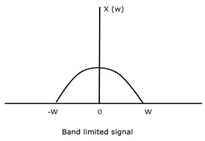
To understand this sampling theorem, let us consider a band-limited signal between –W and W Hz, that is, a signal whose value is non-zero, is represented as
x(f)=0 for|f|>W
The x (t): the continuous-time signal can be represented in the in frequency domain, i.e. in the form of Band limited signal, as shown if figure below,
We required a sampling frequency, such that at that frequency there should be no loss of information, even after sampling. Nyquist rate is used for this, i.e. sampling frequency should be two times the maximum frequency. This is the critical rate of sampling.
If the signal x(t) is sampled above value of the Nyquist rate, the original signal can be recovered, and if it is sampled below the value of Nyquist rate, the signal cannot be recovered.
When signal is sampled at a higher rate than 2w in the frequency domain, that signal can be represented as shown in following figure,
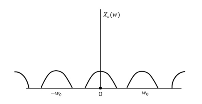
The above figure shows the F.T. i.e. Fourier transform of a signal xs(t). Here, the information is given without any loss. Here signals are not getting missed up and hence recovery is possible.
The Fourier Transform of the signal xs(t) is
Xs(w)=

Where Ts is Sampling Period and w0=2πTs
Let us see what happens if the sampling rate fs is equal to two times the highest frequency 2W
That means,
fs = 2W
Where,
fs: sampling frequency
W: highest frequency
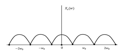
The above figure shows the result. The information is replaced without any loss. Hence, this sampling rate is also good.
Now, let us look at the condition,
fs < 2W
The resultant pattern is as shown in figure below,
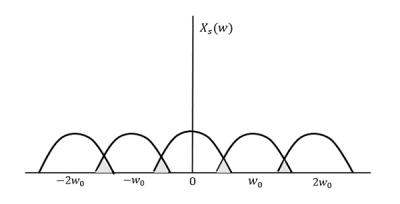
From above pattern we can observe that the information is over-lapped, because of that signals are get mixed and information get loosed. This unwanted over-lapping phenomenon is called as Aliasing.
Aliasing
Aliasing can be referred to as “the phenomenon of a high-frequency component in the spectrum of a signal, taking on the identity of a low-frequency component in the spectrum of its sampled version.”
The corrective measures taken to reduce the effect of Aliasing are −
- In the transmitter section of PCM, a low pass anti-aliasing filter is employed, before the sampler, to eliminate the high frequency components, which are unwanted.
- The signal which is sampled after filtering, is sampled at a rate slightly higher than the Nyquist rate.
This choice of having the sampling rate higher than Nyquist rate, also helps in the easier design of the reconstruction filter at the receiver.
After continuous wave modulation, the Pulse modulation is another type of analog modulation. Now let us see the techniques/ types of analog pulse modulation.
- Pulse Amplitude Modulation (PAM)
- Pulse Width Modulation (PWM)
- Pulse Position Modulation (PPM)
Pulse Amplitude Modulation
In PAM technique, the amplitude of the pulse carrier varies with respect to the instantaneous amplitude of the message signal.
The amplitude of the original signal will be followed by the pulse amplitude modulated signal, as the signal traces out the path of the whole wave. In natural PAM, a signal sampled at Nyquist rate can be reproduced, by passing this signal through a Low Pass Filter (LPF) with exact cutoff frequency.
The Pulse Amplitude Modulation waveforms are as shown in the figure below.
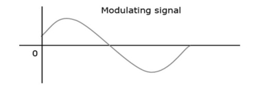
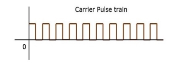

Though Low Pass Frequency passes the low frequency signal below cutoff, it cannot recover the signal without distortion. Hence, to remove this distortion, flat-top sampling is used. The flat-top PAM signal is as shown in the figure.
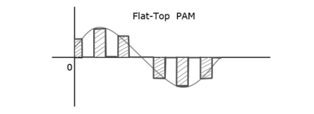
If the pulse is in the form of Flat-top we can remove the noise which is introduced at the top. This process is known as Flat-Top sampling. Sample and hold circuit makes the pulses flat at the top, so this circuit is used for Flat top sampling.
Pulse Width Modulation
The width or the duration or the time of the pulse carrier varies, with respect to the amplitude of the message signal is known as Pulse Width Modulation, which is also called as Pulse Duration Modulation (PDM) or Pulse Time Modulation (PTM).
Here the amplitude of the signal remains constant, only the width of the pulse changes. To make the amplitude constant Amplitude Limiters are used here. This amplitude limiter circuits cut off the amplitude to desire level, and because of that noise is limited.
The figure given below shows the waveforms of Pulse Width Modulations.
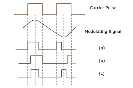
There are 3 types of PWM.
- Taking the starting(leading) edge of the pulse constant, the trailing edge varies according to the message signal. Fig (a) in above figure shows this type of waveforms.
- Taking the dragging(trailing) edge of the pulse constant, the leading edge varies according to the message signal. Fig (b) in the above figure shows this type of waveforms.
- Taking the midpoint (center) of the pulse as constant, the leading edge and the trailing edge varies according to the message signal. Fig (c) in the above figure shows this type of waveforms.
Pulse Position Modulation
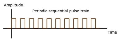
When position of the pulses with reference to the position of a reference pulse varies with respect to sampled value of the message signal is known as Pulse Position Modulation (PPM). Here the amplitude and width are constant.
To keep the transmitter and receiver in synchronization, the transmitter has to send sync pulses. These sync pulses maintain the position of the pulses. The fig given below shows the waveforms of Pulse Position Modulation.

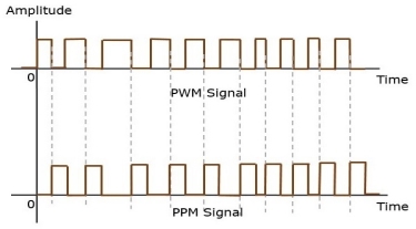
Pulse position modulation is done with respect to the pulse width modulated signal. Each dragging(trailing) edge of the pulse width modulated signal becomes the starting point for pulses in PPM signal. Hence, the position of all those pulses is proportional to the width of the PWM pulses.
Advantage
The power handled is also constant, because the amplitude and the width are constant,
Disadvantage
Transmitter and the receiver synchronization is a must.
Comparison between PAM, PWM, and PPM.
PAM | PWM | PPM |
Vary the Amplitude | Vary the Width | Vary the Position |
The width of the pulse decides the BW. | The rise time of the pulse decides the BW | The rise time of the pulse decides the BW |
As amplitude of pulses vary instantaneous transmitter power also varies | As amplitude and width of pulses vary instantaneous transmitter power also varies | Width of the pulses constant so instantaneous transmitter power remains constant |
Complexity of system is high | Complexity of system is low | Complexity of system is low |
High noise interference | Low noise interference | Low noise interference |
It is same to amplitude modulation | It is same to frequency modulation | It is same to phase modulation |
Modulation is the process of varying one or more parameters like amplitude frequency, phase, position of a carrier signal with respect to the the instantaneous values of the message signal.
The message signal is the signal which contains the data used for communication and the carrier signals have high frequency which is used to transmit the message signal for long distance.
We have already seen the types of modulation. We have learnt the analog modulation techniques. For digital modulation, technique used is Pulse Code Modulation PCM.
In PCM, the analog information is converted into binary form i.e. in 1s and 0s form. The fig given below shows an example of PCM output.
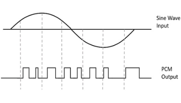
PCM produces a high and low levels i.e. digits instead of pulse train and hence this process is digital. Each levels or digits, though in binary code, represent the approximate amplitude of the signal sample at that time.
In Pulse Code Modulation, a sequence of coded pulses represents the message signal. This message signal is reproduced by representing the signal in discrete form in both time and amplitude.
Basic Elements of PCM
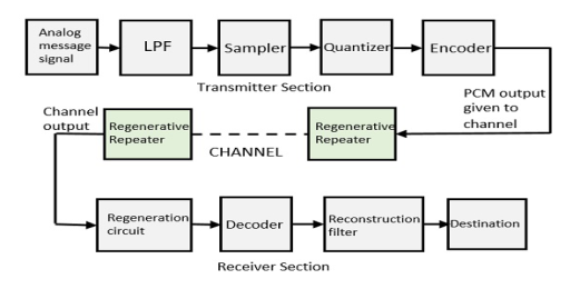
Sampling, Quantizing and Encoding are the main blocks of the transmitter section of a Pulse Code Modulator circuit. These processes are performed in the analog-to-digital converter section. For the prevention of aliasing of message signal, the low pass filter is used to sampling.
Regeneration of impaired signals, decoding, and reconstruction of quantized pulse train are the basic operations of receiver section. The block diagram of PCM transmitter and receiver is as shown in fig below.
Low Pass Filter
Low Pass Filter passes the low frequency components and removes the high frequency components which is greater than the highest frequency of message signal. It avoid aliasing of information signal.
Sampler
Sampler collect the sample data at instantaneous values of message signal, so as to regain the original signal. The sampling rate should be > 2W of message signal, as given in sampling theorem.
Quantizer
To reduce the excessive bits and confining the data Quantization process is used. Quantizer compresses the value by reducing the redundant bits of the sampled output.
Encoder
Encoder does the digitization of analog signal. Sample and hold process is used for sampling. The three sections LPF, Sampler, and Quantizer LPF, Sampler, and Quantizer are used to convert an analog signal to digital signal. Encoding minimize the BW.
Regenerative Repeater
Regenerative Repeater section increases the signal strength. The output of the channel also has one regenerative repeater circuit, To avoid the signal loss and regain the signal, the output of channel has one regenerative circuit and it increases the strength of signal also.
Decoder
To regain the original signal and to decode the pulse coded waveform, the decoder circuit is used. Decoder circuit acts as the demodulator.
Reconstruction Filter
Regenerative circuit and decoder circuit decode the signal and pass that signal to low-pass filter, which is known as reconstruction filter to regain the original signal.
The analog wave (signal) is digitalized by Pulse Code Modulator circuit. This circuit codes is, samples it in digital form. To receive the original analog signal the whole process is repeated in reverse pattern.
Digital-to-Analog conversion is also equally important in this digital modulation. The techniques used for this conversion are known as Digital Modulation techniques.
Providing more information capacity, high data security, quicker system availability with great quality communication are the main advantages of Digital Modulation. Therefore, digital modulation techniques are used for many applications.
Depending upon the need, digital modulation are classified in to many techniques. Some of them which are prominent are given below.
ASK – Amplitude Shift Keying
Name itself indicates that the amplitude of the output gets changed with the input data whether it should be a zero level or a variation of positive and negative, depending upon the carrier frequency.
FSK – Frequency Shift Keying
As it is Frequency Shift Keying the frequency of the output signal becomes either high or low, which depends upon the input data applied.
PSK – Phase Shift Keying
Here the phase of the output signal gets shifted with respect to the input. Depending upon the number of phase shifts, there are two types of phase shift, namely Binary Phase Shift Keying BPSK and Quadrature Phase Shift Keying QPSK. When output signal changes the phase according to the previous value is known as Differential Phase Shift Keying DPSK.
M-ary Encoding
M-ary Encoding techniques is used to transmit more than two bits simultaneously on a single signal. This helps within the reduction of bandwidth.
The M-ary techniques can be classified as −
- M-ary ASK
- M-ary FSK
- M-ary PSK
This is type of digital modulation in which amplitude of the carrier signal is varying with respect to changes in digital signal and it is represented in binary data form.
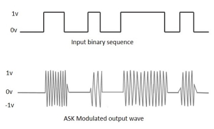
ASK modulated signal gives high frequency output i.e. carrier output for High input i.e. for 1V input, and gives no value or zero value when input is Low i.e. 0V.
The waveforms given below shows the ASK modulated waveforms with input signal,
ASK Modulator
The figure given below shows the block diagram of the ASK Modulator.
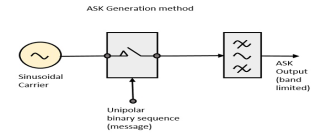
ASK modulator be made up of the carrier signal generator, the binary sequence from the message signal and the band-limited filter.
The carrier generator, generates a continuous high-frequency carrier signal. The binary sequence from the message signal generates unipolar input which is in the form of High or Low signal. When the signal input is high, it closes the switch, carrier waves passes through the circuit. So, the output is the carrier signal at high input. When signal input is low input, the switch remains opens, no signal passes through the circuit. So, the output is low at low input.
The band-limiting filter which is also known as pulse-shaping filter, gives shape to the waveform of transmitted pulse depending upon the amplitude and phase characteristics of that filter.
ASK Demodulator
There are two types of ASK Demodulation techniques. They are −
- Asynchronous ASK Demodulation/detection
- Synchronous ASK Demodulation/detection
When the clock frequency at the transmitter is equal to the clock frequency at the receiver, it is known as a Synchronous method, as the frequency gets synchronized. Otherwise, it is known as Asynchronous.
Asynchronous ASK Demodulator
The Asynchronous ASK detector made up of a half-wave rectifier, a low pass filter, and a comparator. The figure given below shows the block diagram of ASK Demodulator,
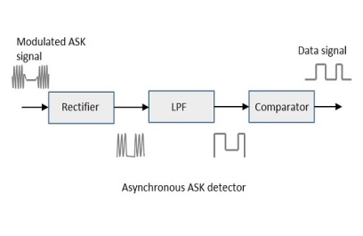
The half-wave rectifier receives the output ASK signal and delivers a positive half output. The low pass filter passes the low frequencies by suppressing the higher frequencies. The output of LPF is given to the comparator which delivers a digital output.
Synchronous ASK Demodulator
Synchronous ASK detector contains a Square law detector, low pass filter, a comparator, and a voltage limiter. The fig given below shows the block diagram for the same.
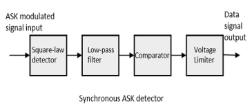
Square law detector receives the ASK modulated signal as input. The output voltage of a square law detector is proportional to the square of the amplitude modulated input voltage. The low pass filter passes the low frequencies by suppressing the higher frequencies. The comparator and the voltage limiter gives a clean digital output.
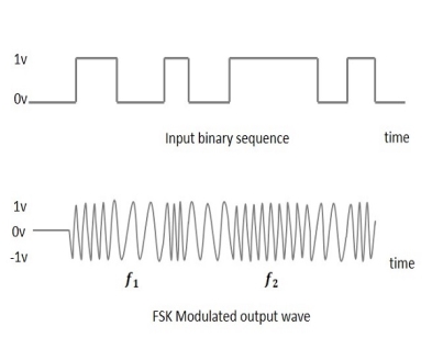
This is type of digital modulation in which frequency of the carrier signal is varying with respect to changes in digital signal.
ASK modulated signal gives high frequency output i.e. carrier output for High input i.e. for 1V or high binary input, and gives low frequency output value when input is Low i.e. 0V. The binary 1s are called Mark frequencies and 0s are called Space frequencies
The waveforms given below shows the FSK modulated waveforms with input signal,
 .
.
FSK Modulator
FSK modulator be made up of two oscillators with a clock and the input binary sequence. The figure given below shows the block diagram of the ASK Modulator.
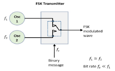
The two oscillators, gives a higher and a lower frequency signals, and that frequencies are connected to a switch along with an internal clock. To avoid the sudden or unexpected phase discontinuities of the output waveform during the transmission of the message, a clock is applied to both the oscillators, internally. The binary input sequence is applied to the transmitter so as to choose the frequencies considering the binary input
FSK Demodulator
There are two types of FSK Demodulation techniques. They are −
- Asynchronous FSK Demodulation/detection: Non-coherent detection.
- Synchronous FSK Demodulation/detection: Coherent detection.
Asynchronous FSK Detector
Asynchronous FSK detector contains two band pass filters, two envelope detectors, and a decision circuit. The fig given below shows the diagrammatic representation.
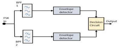
The FSK signal is given to the two Band Pass Filters BPFs as an input, that is tuned to Space and Mark frequencies. The output of these two BPFs is like ASK signal, this ASK signal is given to the envelope detector. Asynchronously modulated signal is given out through envelope detector.
We get the two asynchronously modulated signal, out of that one output is selected by the decision circuit. This circuit chooses which output is more suitable and selects it from any one of the envelope detectors. The decision circuit re-shapes the waveform to a rectangular one.
Synchronous FSK Detector
Synchronous FSK detector contains two mixers with local oscillator circuits, two band pass filters and a decision circuit. The figure given below shows the diagrammatic representation of Synchronous FSK Detector.
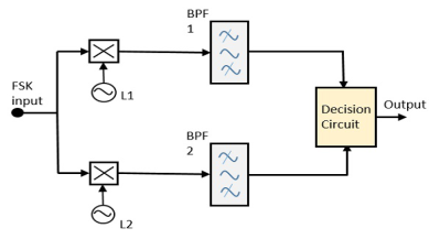
The FSK signal input is passed to the two mixers with local oscillator circuits, which are connected to two band pass filters. These combinations of ‘local oscillator and bandpass filter’ act as demodulators and the decision circuit chooses which output is more suitable and selects it from any one of the detectors. The 2 signals have a minimum frequency separation.
The bandwidth of each of both of the demodulators depends on their bit rate. This synchronous demodulator is difficult or complex than asynchronous type demodulators.
This is type of digital modulation in which phase of the carrier signal is varying with respect to changes the sine and cosine inputs at a particular time. Applications are PSK are:
1) Used for wireless LANs.
2) For bio-metric use.
3) For contactless operations
4) For RFID and Bluetooth communications.
Basically there are two types of PSK, depending upon the phases the signal gets shifted. They are –
Binary Phase Shift Keying BPSK
Quadrature Phase Shift Keying QPSK
3.7.1 Binary Phase Shift Keying BPSK
This is also known as 2-phase PSK or Phase Reversal Keying. In this technique, the sine wave carrier takes 2 phase reversals such as 0° and 180°.
BPSK basically a follows DSBSC modulation scheme, for message being the digital information.
BPSK Modulator
The basic block present in Binary Phase Shift Keying is the balance modulator which has the carrier sine wave as one input and the binary sequence as the other input. The fig given below shows the diagrammatic representation of BPSK modulator.
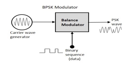
The two inputs i.e. binary data and carrier waves are given to the balance modulator, which multiplies these two signals ang gives modulated output. If the binary input is zero, the phase will be 0° and If the binary input is high, the phase reversal is of 180°.
The fig given below shows the waveforms of BPSK along with input.
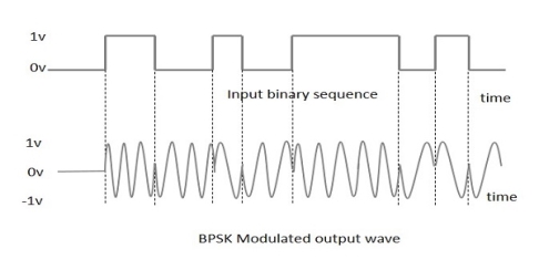
Sine wave is the output of the modulator, which will be the direct input carrier or the inverted 180° phase shifted input carrier, which is a function of the data signal.
BPSK Demodulator
The block diagram of BPSK demodulator contains a mixer with local oscillator circuit, a bandpass filter, a two-input detector circuit. Block digram of same is as shown in fig.
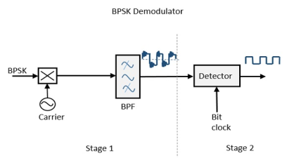
Mixer circuit and band pass filter recover the band-limited message signal, and complete the first stage of demodulation. The band limited base band signal is obtained which is used to regenerate the binary message bit stream.
To produce the original binary message signal, the detector circuit needs bit clock rate, which is the next stage of modulation. The sub-multiple bit rate of carrier frequency simplifies the bit clock regeneration. The decision making circuit at the 2nd stage makes the circuit easily understandable.
3.7.2 Quadrature Phase Shift Keying QPSK
In this phase shift keying technique, sine wave carrier takes 4 phase reversals such as 0°, 90°, 180°, and 270°.
If this type of techniques are further extended, PSK are often done by eight or sixteen values also, depending upon the need.
The QPSK is a variation of BPSK, and it also basically follows DSBSC modulation scheme. As message contains the digital information, which sends two bits of digital information at a time, called as bigits.
QPSK converts digital bits into digital pairs, instead of series of digital stream. Because of that data bit rate decreases to half, which gives space for the other users.
QPSK Modulator
The QPSK Modulator contains a bit-splitter, two multipliers with local oscillator, a 2-bit serial to parallel converter, and a summer circuit. The fig given below shows the block diagram for the same.
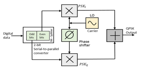
At the modulator’s input, the bits splitter separates the even bits (i.e., 2nd bit, 4th bit, 6th bit, etc.) and odd bits (i.e., 1st bit, 3rd bit, 5th bit, etc.) of message signal. These signals are multiplied with the carrier to generate odd BPSK (called as PSKI) and even BPSK (called as PSKQ). Before signal gets modulated, the PSKQ signal is phase shifted by 90°.
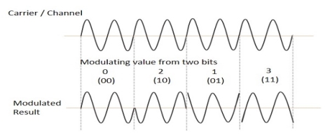
The QPSK waveform are as shown in given below for two-bits input. For different instances of binary inputs, the modulated result is given.
QPSK Demodulator
The QPSK Demodulator contains 2 product demodulator circuits with local oscillator, 2 band pass filters, 2 integrator circuits, and a 2-bit parallel to serial converter. Following is the diagram for the same.
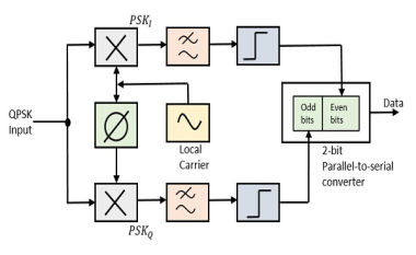
The two product detectors at the input of demodulator simultaneously demodulate the 2 BPSK signals. The pair of bits are recovered here from the first i.e. original data. These signals after processing, are passed to the parallel to serial converter.
Reference Books:
- Dr. Sanjay Sharma, “Communication System (Analog and Digital)”, Katson Books.
- Simon Haykins, ‘Communication Systems’, John Wiley, 3rd Edition, 1995.
- Kennedy G, ‘Electronic Communication System’, McGraw Hill, 1987.