Unit - 2
COMBINATIONAL MOS LOGIC CIRCUITS
A static CMOS gate is a combination of two networks, called the pull-up network (PUN) and the pull-down network (PDN). The figure shows a generic N input logic gate where all inputs are distributed to both the pull-up and pull-down networks. The function of the PUN is to provide a connection between the output and VDD anytime the output of the logic gate is meant to be 1. Similarly, the function of the PDN is to connect the output to VSS when the output of the logic gate is meant to be 0.
The PUN and PDN networks are constructed in a mutually exclusive fashion such that one and only one of the networks is conducting in steady state. In this way, once the transients have settled, a path always exists between VDD and the output F, realizing a high output, or, alternatively, between VSS and F for a low output. This is equivalent to stating that the output node is always a low-impedance node in steady state. In constructing the PDN and PUN networks, the following observations should be kept in mind:
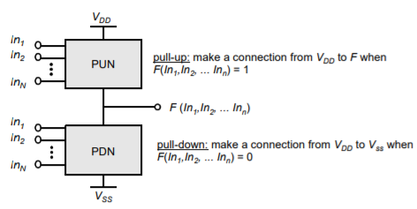
Fig 1 Complementary logic gate as a combination of a PUN (pull-up network) and a PDN (pull-down network).
A transistor can be thought of as a switch controlled by its gate signal. An NMOS switch is on when the controlling signal is high and is off when the controlling signal is low. A PMOS transistor acts as an inverse switch that is on when the controlling signal is low and off when the controlling signal is high.
The PDN is constructed using NMOS devices, while PMOS transistors are used in the PUN. The primary reason for this choice is that NMOS transistors produce strong zeros, and PMOS devices generate strong ones.
Key takeaway
A static CMOS gate is a combination of two networks, called the pull-up network (PUN) and the pull-down network (PDN).
The CMOS logic style described in the previous section is highly robust and scalable with technology, but requires 2N transistors to implement a N-input logic gate. Also, the load capacitance is significant since each gate drives two devices (a PMOS and an NMOS) per fan-out. Ratioed logic is an attempt to reduce the number of transistors required to implement a given logic function, at the cost of reduced robustness and extra power dissipation. The purpose of the PUN in complementary CMOS is to provide a conditional path between VDD and the output when the PDN is turned off. In ratioed logic, the entire PUN is replaced with a single load device that pulls up the output when the PDN is turned off.
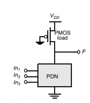
Fig 2 Ratioed Logic Gate
Above figure shows an example of ratioed logic which uses a grounded PMOS load and referred to as a pseudo-NMOS style. Instead of a combination of active pull-down and pull-up networks, such a gate consists of an NMOS pull-down network that realizes the logic function, and a simple load device.
The clear advantage of pseudo-NMOS is the reduced number of transistors (N+1 vs. 2N for complementary CMOS). The nominal high output voltage (VOH) for this gate is VDD since the pull-down devices is turned off when the output is pulled high (assuming that VOL is below VTn). On the other hand, the nominal low output voltage is not 0V since there is a fight between the devices in the PDN and the load grounded PMOS device. This results in reduced noise margins and more importantly static power dissipation. The sizing of the load device relative to the pull-down devices can be used to trade-off parameters such a noise margin, propagation delay and power dissipation. Since the voltage swing on the output and overall functionality of the gate is dependent on the device size, the circuit is called ratioed. This is in contrast to the ratioless logic styles, such as complementary CMOS, where the low and high levels do not depend upon transistor sizes.
g the dc transfer characteristic of the pseudo-NMOS proceeds along paths similar to those used for its complementary CMOS counterpart. The value of VOL is obtained by equating the currents through the driver and load devices for Vin = VDD. At this operation point, it is reasonable to assume that the NMOS device resides in linear mode (since the output should ideally be close to 0V), while the PMOS load is saturated

Assuming that VOL is small relative to the gate drive (VDD-VT) and that VTn is equal to VTp in magniture, VOL can be approximated as:

In order to make VOL as small as possible, the PMOS device should be sized much smaller than the NMOS pull-down devices. Unfortunately, this has a negative impact on the propagation delay for charging up the output node since the current provided by the PMOS device is limited.
An important disadvantage of pseudo-NMOS gates is static power that happens when the output is low, because a direct current path exists between VDD and GND through the load and driver devices. The static power consumption in the low-output mode is easily derived

Key takeaway
Ratioed logic is an attempt to reduce the number of transistors required to implement a given logic function
We can understand this logic configuration as an attempt to improve pseudo-nMOS logic circuits. Consider the NOR gate shown below: Static power is consumed by this NOR circuit whenever the output is ‘LOW’. This happens when A OR B is TRUE. We wish that the pMOS could be turned off for just this combination of inputs. To turn the pMOS transistor off, we need to apply a ‘HIGH’ voltage level to its gate whenever A OR B is true. This obviously requires an OR gate. Non-inverting gates cannot be made in a single stage as shown below.
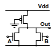
Fig 3 Pseudo-nMOS NOR

Fig 4 Pseudo-nMOS OR from complemented inputs
We want to turn the pMOS of this OR circuit off when both A and B are ‘HIGH’; i.e. when  =
=  = 0. This means we would like to turn the pMOS of this circuit off when the NOR of A and B is ‘TRUE. But we already have this signal as the output of the first (NOR) circuit! So the two circuits can drive each other’s pMOS transistors and avoid static power consumption. This kind of logic is called Cascade Voltage Switch Logic (CVSL).
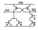
Fig OR-NOR implementation in Cascade Voltage Switch Logic
We can use any network f and its complementary network f in the two cross-coupled branches. The complementary network is constructed by changing all series connections in f to parallel and all parallel connections to series, and complementing all input signals.
Key takeaway
CVSL shares many characteristics with static CMOS, CPL and pseudo-nMOS.
• As CMOS static logic, there is no static power consumption.
• As CPL, this logic requires both True and Complement signals. It also provides both True and complement outputs. (Dual Rail Logic).
• Like pseudo nMOS, the inputs present a single transistor load to the driving stage.
• The circuit is self-latching. This reduces ratioing requirements.
The basic construction of a N-type dynamic logic gate is shown in Figure below. The PDN (pull-down network) is constructed exactly in the same fashion as a complementary CMOS. The operation of this circuit can be divided into two major phases: pre-charge and evaluation, with the mode of operation determined by the clock signal.
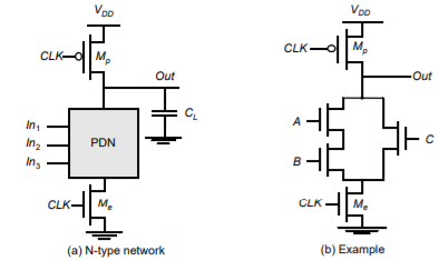
Fig 5 Basic concept of dynamic gate
When CLK = 0, the output node Out is pre-charged to VDD by the PMOS transistor Mp. During that time, the evaluate NMOS transistor Me is off, so the pull-down path does not fight the pull-up path. The evaluation FETS also eliminate any static power that would be consumed during the pre-charge period (i.e., if the pull-down path was turned on and the pre-charge device was turned on, static current would flow between the supplies.
When CLK = 1, the precharge transistor Mp is off, and the evaluation transistor Me is turned on. The output is conditionally discharged based on the input values and the pulldown topology. If the inputs are such that the PDN conducts, then a low resistance path exists between Out and GND and the output is discharged to GND. If the PDN is turned off, the precharged value remains stored on the output capacitance CL, which is a combination of junction capacitances, the wiring capacitance, and the input capacitance of the fanout gates. During the evaluation phase, the only possible path between the output node and a supply rail is to GND.
Consequently, once Out is discharged, it cannot be charged again till then next precharge operation. The inputs to the gate can therefore make at most one transition during evaluation. Notice that the output can be in the high impedance state during the evaluation period if the pull-down network is turned off and this behaviour is fundamentally different than the static counterpart that always has a low resistance path between the output and one of the power rails.
As as an example of dynamic logic, consider the circuit shown in Figure b. During the precharge phase (CLK=0), the output is precharged to VDD regardless of the input values since the evaluation device is turned off. During evaluation (CLK=1), a conducting path is created between Out and GND if (and only if) A·B+C is TRUE. Otherwise, the output remains at the precharged state of VDD. The following function is thus realized:
Out =  when CLK =1
A number of important properties can be derived for the dynamic logic gate:
• The logic function is implemented by the NMOS pull-down network. The construction of the PDN proceeds just as it does for static CMOS.
• The number of transistors (for complex gates) is substantially lower than in the static case: N + 2 versus 2N.
• It is non ratioed. The sizing of the PMOS precharge device is not important for realizing proper functionality of the gate. The size of the precharge device can be made large to improve the low-to-high transition time (of course, at a cost to the high-to low transition time). There is however, a trade-off with power dissipation since a larger precharge device directly increases clock power dissipation.
• It only consumes dynamic power. Ideally, no static current path ever exists between VDD and GND. The overall power dissipation, however, can be significantly higher compared to a static logic gate.
• The logic gates have faster switching speeds. There are two main reasons for this. The first reason is due to the reduced load capacitance attributed to the number of transistors per gate and the single-transistor load per fan-in. Second, the dynamic gate does not have short circuit current, and all the current provided by the pull-down devices go into discharging the load capacitance.
Key takeaway
The operation of this circuit can be divided into two major phases: pre-charge and evaluation, with the mode of operation determined by the clock signal.
A popular and widely used alternative to complementary CMOS is pass transistor logic. Pass transistor logic attempts to reduce the number of transistors required to implement logic by allowing the primary inputs to drive gate terminals as well as source/drain terminals. This is in contrast to logic families that we have studied so far that only allow primary inputs to drive the gate terminals of MOSFETS.
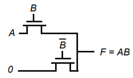
Fig 6 Pass Transistor Implementation of an AND gate
Figure above shows a transistor level implementation of the AND function constructed using NMOS transistors. In this gate, if the B input is high, the top transistor is turned on and copies the input A to the output F. When input B is low, the bottom pass transistor is turned on and passes a 0. The switch driven by B seems to be redundant at first glance. Its presence is essential to ensure that a low-impedance path exists to the supply rails under all circumstances, or, in this particular case, when B is low.
The potential advantage of pass transistor is that a fewer number of transistors are required to implement a given function. For example, the implementation of the AND gate in Figure above requires 4 transistors (including the inverter required to invert B) while a complementary CMOS implementation would require 6 transistors. Pass transistor logic uses fewer devices and therefore has lower physical capacitance. Unfortunately, as we have discussed earlier, a NMOS device is effective at passing a 0 but is poor at pulling a node to VDD. In pass transistor logic, the pass transistors are used to pass high and low voltages. Therefore, when the pass transistor pulls a node high, the output only charges up to VDD -VTn. In fact, the situation is worsened by the fact that the devices experience body effect since there is a significant source to body voltage when pulling high since the body is tied to GND and the source charge up close to VDD.
Consider the case when the pass transistor is charging up a node to VDD where the gate and drain terminals are set at VDD. Let the source the NMOS pass transistor be labelled x. Node x will charge up to VDD-VTn where, the threshold must account for body effect as shown in equation below. This maximum voltage swing on the output node is given by

Key takeaway
Pass transistor logic attempts to reduce the number of transistors required to implement logic by allowing the primary inputs to drive gate terminals as well as source/drain terminals. This is in contrast to logic families that we have studied so far that only allow primary inputs to drive the gate terminals of MOSFETS.
The most widely used solution to deal with the voltage drops induced by pass transistors are the use of transmission gates. The primary limitation of NMOS or PMOS only pass gate is the threshold drop (NMOS pass device pass a strong 0 while passing a week 1 and PMOS pass devices pass a strong 1 while passing a weak 0). The ideal approach is to use the NMOS device to pull-down and the PMOS device to pull-up. The transmission gate combines the best of both device flavours by placing a NMOS device in parallel with a PMOS device (Figure a). The control signals to the transmission gate (C and C) are complementary. The transmission gate acts as a bidirectional switch controlled by the gate signal C. When C = 1, both MOSFETs are on, allowing the signal to pass through the gate. In short,
A=B
If C=1
On the other hand, C = 0 places both transistors in cut-off, creating an open circuit between nodes A and B. Figure below shows a commonly used transmission-gate symbol
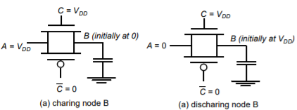
Fig 7 Transmission gates enable rail-to-rail switching
Transmission gates can be used to build some complex gates very efficiently. Figure below shows an example of a simple inverting two-input multiplexer. This gate either selects input A or B based on the value of the control signal S, which is equivalent to implementing the following Boolean function:
 = (A. S + B
  )
)
A complementary implementation of the gate requires eight transistors instead of six
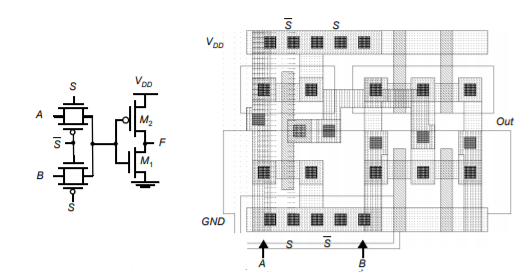
Fig 8 Transmission gate multiplexer and its layout
Key takeaway
The primary limitation of NMOS or PMOS only pass gate is the threshold drop (NMOS pass device pass a strong 0 while passing a week 1 and PMOS pass devices pass a strong 1 while passing a weak 0). The ideal approach is to use the NMOS device to pull-down and the PMOS device to pull-up. The transmission gate combines the best of both device flavours by placing a NMOS device in parallel with a PMOS device
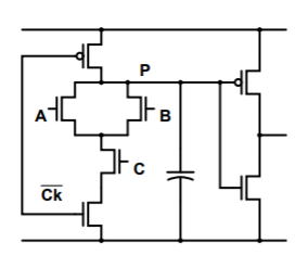
Fig 9 CMOS Domino logic
Another way to eliminate the problem with cascading logic stages is to use a static inverter after the CMOS dynamic gate. Recall that the cascaded dynamic CMOS stage causes problems because the output is pre-charged to Vdd. If the final value is meant to be zero, the next stage nMOS to which the output is connected erroneously sees a one till the pre-charged output is brought down to zero. During this time, it ends up discharging its own pre-charged output, which it was not supposed to do. If an inverter is added, the output is held ‘low’ before logic evaluation. If the final output is zero, there is no problem anyway. If the final output is supposed be one, the next stage is erroneously held at zero for some time. However, this does not result in a false evaluation by the next stage. The only effect it can have is that the next stage starts its evaluation a little later. However, the addition of an inverter means that the logic is non-inverting. Therefore, it cannot be used to implement any arbitrary logic function.
Key takeaway
If the final value is meant to be zero, the next stage nMOS to which the output is connected erroneously sees a one till the pre-charged output is brought down to zero. During this time, it ends up discharging its own pre-charged output, which it was not supposed to do.
The idea of Dual-rail logic is to use two semiwires per variable. Each wire either holds the value TRUE or doesn’t. The choice of which wire holds the value TRUE corresponds with the value of the variable. This is in contrast to Binary logic which represents each variable as a single wire which can hold either TRUE or FALSE values. Domino circuits that generate both polarities of output are called dual rail domino.
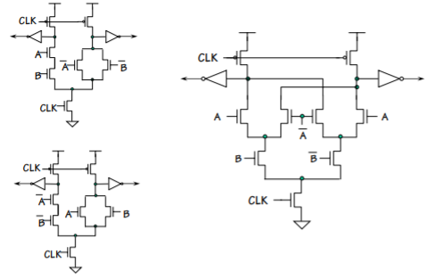
Fig 10 Dual rail domino
This logic family is based on multiplexer logic. Given a Boolean function F (x1, x2, . . . , xn), we can express it as:
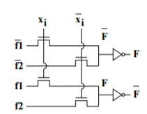
Fig 11 Basic Multiplexer with logic restoring inverters
F (x1, x2, . . . , xn) = xi · f1 + xi’ · f2
where f1 and f2 are reduced expressions for F with xi forced to 1 and 0 respectively. Thus, F can be implemented with a multiplexer controlled by xi which selects f1 or f2 depending on xi. f1 and f2 can themselves be decomposed into simpler expressions by the same technique. To implement a multiplexer, we need both xi and xi’. Therefore, this logic family needs all inputs in true as well as in complement form. In order to drive other gates of the same type, it must produce the outputs also in true and complement forms. Thus, each signal is carried by two wires. This logic style is called Complementary Pass gate Logic or CPL.
Pure pass gate logic contains no ‘amplifying’ elements. Therefore, it has zero or negative noise margin. (Each logic stage degrades the logic level). Therefore, multiple logic stages cannot be cascaded. We shall assume that each stage includes conventional CMOS inverters to restore the logic level. Ideally, the multiplexer should be composed of complementary pass gate transistors. However, we shall use just n channel transistors as switches for simplicity as shown in figure above.
Key takeaway
To implement a multiplexer, we need both xi and xi’. Therefore, this logic family needs all inputs in true as well as in complement form. In order to drive other gates of the same type, it must produce the outputs also in true and complement forms.
The Differential Cascade Voltage Switch with Pass-Gate uses nMOS pass-transistor network with cross-coupled pMOS load. The basic AND/NAND, OR/NOR and XOR/XNOR gates implemented in DCVSPG are shown in Figure below.
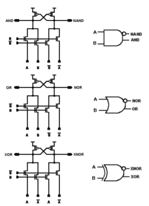
Fig 12 Basic AND/NAND, OR/NOR and XOR/XNOR gates implemented in CVSL
DCVSPG is nothing but CVSL with the nMOS evaluation tree replaced with pass-gate design. Even here the cross coupled pMOS transistors are used. The use of pass-transistor network will improve the speed performance and the decreases power consumption as compared to CVSL. This logic also eliminates the floating node problem caused by CVSL by replacing the differential pairs of nMOS transistors with a pass-transistor gate design.
The pull-up performance is contributed both from pMOS and nMOS transistors, an increase in pMOS transistor width will improve the pull-up performance. However, the increased pMOS transistor junction capacitance will degrade the pulldown performance. Hence for optimum performance the pMOS to nMOS ratio is chosen to be one.
DPL was introduced and like CPL it uses complementary signals to drive the logic cells. As with CPL only a limited number of simple cells are needed to describe general logic functions. DPL's main difference to CPL, is that it gives full swing signals for every logic state (either an n-mos tree for a logic zero or a p-mos tree for a logic 1 is active). This is very important when looking into reduced supply voltage designs. CPL's Vt voltage drop, because of pure n-mos logic, is one of its biggest disadvantages and leads to performance degradation and severe design limitations. Buffers have to be inserted to drive the gates of logic cells in order to avoid even further speed degradation. Since DPL has full voltage swing output signals, buffers can be inserted wherever they offer better performance. The added transistor count is a disadvantage over CPL, but the overall advantages in speed can outweigh the increase in power dissipation and area. In fact, power dissipation for DPL is not much worse than CPL, due to the sharper signal rise and fall and better synchronisation of the complementary signals.
The circuit pitfalls can be avoided by managing with the bad circuit designs. The following are bad circuit designs with the solutions on how to overcome the pit fall.
Bad Circuit 1
Circuit – 2:1 multiplexer

Principle: Threshold drop
– X never rises above VDD-Vt
– Vt is raised by the body effect
– The threshold drop is most serious as Vt becomes a greater fraction of VDD
Symptom
– Mux works when selected D is 0 but not 1
– Or fails at low VDD D0 X
– Or fails in SFSF corner
Solution: Use transmission gates, not pass transistors
Bad Circuit 2
Circuit: Latch

Principle: Leakage
– X is a dynamic node holding value as charge on the node
– Eventually subthreshold leakage may disturb charge
Symptom
– Load a 0 into Q
– Set f = 0
– Eventually Q spontaneously flips to 1
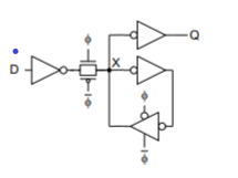
Solution: Refresh node with feedback
– Or periodically refresh node (requires fast clock, not practical processes with big leakage)
Bad Circuit 3
Circuit – Domino AND gate
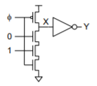
Principle: Leakage
– X is a dynamic node holding value as charge on the node
– Eventually subthreshold leakage may disturb charge
Symptom
– Precharge gate (Y=0)
– Then evaluate
– Eventually Y spontaneously flips to 1
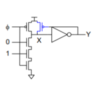
Solution: Keeper
Bad Circuit 4
Circuit – Pseudo-nMOS OR
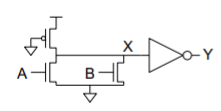
Principle: Ratio Failure
– nMOS and pMOS fight each other.
– If the pMOS is too strong, nMOS cannot pull X low enough.
Symptom
–When only one input is true, Y = 0
– Perhaps only happens in SF corner
Solution: Check that ratio is satisfied in all corners
Bad Circuit 5
Circuit – Latch

Principle: Ratio Failure (again)
– Series resistance of D driver, wire resistance, and pass-gate must be much less than weak feedback inverter.
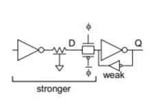
Symptom
– Q stuck at 1.
– May only happen for certain latches where input is driven by a small gate located far away.
Solutions: Check relative strengths
– Avoid un-buffered diffusion inputs where driver is unknown
Bad Circuit 6
Circuit – Domino AND gate
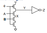
Principle: Charge Sharing
– If X was low, it shares charge with Y
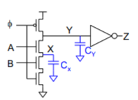
Symptom
– Precharge gate while
– A = B = 0, so Z = 0
– Set f = 1
– A rises
– Z is observed to sometimes rise
Solutions: Limit charge sharing
– Safe if CY >> CX
Vx = Vy = [Cy/Cx +Cy] *VDD
--Or precharge node X too
Bad Circuit 7
Circuit – Dynamic gate + latch
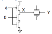
Principle: Charge Sharing
– If Y was low, it shares charge with X
Symptom
– Precharge gate while transmission gate latch is opaque
– Evaluate
– When latch becomes transparent, X falls
Solution: Buffer dynamic nodes before
– driving transmission gate
Bad Circuit 8
Circuit – Latch
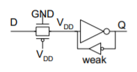
Principle: Diffusion Input Noise Sensitivity
– If D < -Vt, transmission gate turns on
– Most likely because of power supply noise or coupling on D
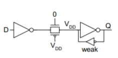
Symptom
– Q changes while latch is opaque
– Especially if D comes from a far-away driver
Solution: Buffer D locally
Bad Circuit 9
Circuit – Anything
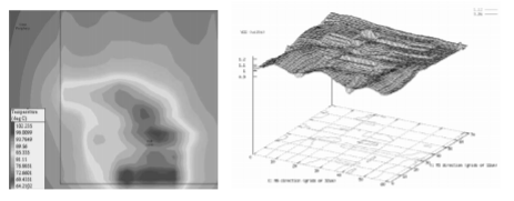
Symptom
– Some gates are slower than expected
Bad Circuit 10: Extremely Large Gate Delays

Node with very large gate delays are susceptible to noise.
Bad Circuit 11: Dog-Bone Devices in Forward Path
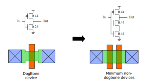
Dog-Bone devices and non-minimum length devices have very large variations in their delay and should only be used for keepers.
Bad Circuit 12: Charge Sharing Tristates
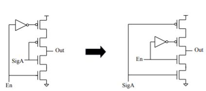
Placing data on the inside of a tristate allows charge sharing as well as extra capacitance on the output.
Bad Circuit 13: Contending Pass Gate Mux Selects

Pass gate mux selects should be designed to all switch at approximately the same time to minimize possible
Bad Circuit 14: Asynchronous Signals Driven from Logic
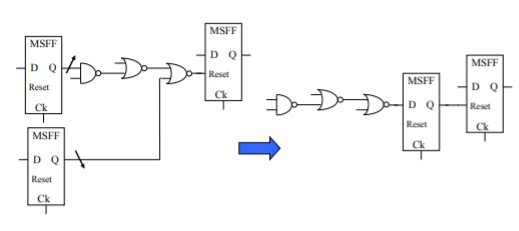
Logic glitches can trigger asynchronous resets improperly.
Bad Circuit 15: Back-writing
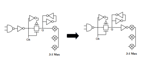
Weakly held nodes driving directly into pass gates can have their data accidentally overwritten.
Bad Circuit 16: Gate-to-Drain Coupling into Weakly Held Node

Weakly held nodes can be disturbed by gate to drain capacitance dramatically increasing gate delay.
Bad Circuit 17: Oversized Keeper in Distributed Domino Gate

Significant RC between the pulldowns can prevent the keeper from being easily overcome. Distributing multiple keepers with the pulldowns can allow for better noise immunity and delay
High frequencies impose a strict limit on power consumption in computer systems as a whole [Ref Texas Instruments]. Therefore, power consumption of each device on the board should be minimized. Power calculations determine power-supply sizing, current requirements, cooling/heatsink requirements, and criteria for device selection. Power calculations also can determine the maximum reliable operating frequency. Two components determine the power consumption in a CMOS circuit:
• Static power consumption
• Dynamic power consumption
CMOS devices have very low static power consumption, which is the result of leakage current. This power consumption occurs when all inputs are held at some valid logic level and the circuit is not in charging states. But, when switching at a high frequency, dynamic power consumption can contribute significantly to overall power consumption. Charging and discharging a capacitive output load further increases this dynamic power consumption. This application report addresses power consumption in CMOS logic families (5 V and 3.3 V) and describes the methods for evaluating both static and dynamic power consumption. Additional information is also presented to help explain the causes of power consumption, and present possible solutions to minimize power consumption in a CMOS system.
Static Power Consumption
Typically, all low-voltage devices have a CMOS inverter in the input and output stage. Therefore, for a clear understanding of static power consumption, refer to the CMOS inverter modes shown in Figure.
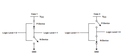
Fig 13 CMOS inverter mode for Static Power Consumption
As shown in Figure above, if the input is at logic 0, the n-MOS device is OFF, and the p-MOS device is ON (Case 1). The output voltage is VCC, or logic 1. Similarly, when the input is at logic 1, the associated n-MOS device is biased ON and the p-MOS device is OFF. The output voltage is GND, or logic 0. Note that one of the transistors is always OFF when the gate is in either of these logic states. Since no current flows into the gate terminal, and there is no dc current path from VCC to GND, the resultant quiescent (steady-state) current is zero, hence, static power consumption (Pq) is zero.
However, there is a small amount of static power consumption due to reverse-bias leakage between diffused regions and the substrate. This leakage inside a device can be explained with a simple model that describes the parasitic diodes of a CMOS inverter, as shown in Figure below.
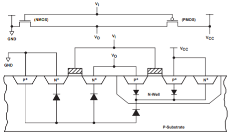
Fig 14 Model Describing Parasitic Diodes Present in CMOS Inverter
The source drain diffusion and N-well diffusion form parasitic diodes. In Figure above, the parasitic diodes are shown between the N-well and substrate. Because parasitic diodes are reverse biased, only their leakage currents contribute to static power consumption. The leakage current (llkg)of the diode is described by the following equation:

Where
 reverse saturation current
V = diode voltage
k= Boltzman’s constant (1.38×
q= electronic charge (1.602 ×  )
)
T = temperature
Static power consumption is the product of the device leakage current and the supply voltage. Total static power consumption, PS, can be obtained as shown in equation
Ps = 
Most CMOS data sheets specify an ICC maximum in the 10-µA to 40-µA range, encompassing total leakage current and other circuit features that may require some static current not considered in the simple inverter model.
The leakage current ICC (current into a device), along with the supply voltage, causes static power consumption in the CMOS devices. This static power consumption is defined as quiescent, or PS, and can be calculated by equation
Ps = Vcc x Icc
VCC = supply voltage
ICC = current into a device
Dynamic Power Consumption
The dynamic power consumption of a CMOS IC is calculated by adding the transient power consumption (PT), and capacitive-load power consumption (PL).
Transient Power Consumption
Transient power consumption is due to the current that flows only when the transistors of the devices are switching from one logic state to another. This is a result of the current required to charge the internal nodes (switching current) plus the through current (current that flows from VCC to GND when the p-channel transistor and n-channel transistor turn on briefly at the same time during the logic transition).
The frequency at which the device is switching, plus the rise and fall times of the input signal, as well as the internal nodes of the device, have a direct effect on the duration of the current spike. For fast input transition rates, the through current of the gate is negligible compared to the switching current. For this reason, the dynamic supply current is governed by the internal capacitance of the IC and the charge and discharge current of the load capacitance. Transient power consumption can be calculated using equation
PT = Cpd x VCC2 x f1 x NSW
Where:
PT = transient power consumption
VCC = supply voltage
fI = input signal frequency
NSW = number of bits switching
Cpd = dynamic power-dissipation capacitance
Capacitive-Load Power Consumption
Additional power is consumed in charging external load capacitance and is dependent on switching frequency. The following equation can be used to calculate this power if all outputs have the same load and are switching at the same output frequency.
PL = CL x VCC2 x fo x NSW (CL is the load per output)
Where:
PL = capacitive-load power consumption
VCC = supply voltage
fO = output signal frequency
CL = external (load) capacitance
NSW = total number of outputs switching
In the case of different loads and different output frequencies at all outputs, above equation is used to calculate capacitive-load power consumption.

Where
 = sum of n different frequencies and loads at n different outputs
 all different output frequencies at each output, numbered 1 through n (Hz)
 supply voltage (V)
 all different load capacitances at each output, numbered 1 through n.
Therefore, dynamic power consumption (PD) is the sum of these two power consumptions and can be expressed as shown


 power- consumption capacitance (F)
 input frequency (Hz)
 all different output frequencies at each output, numbered 1 through n (Hz)
 total number of outputs switching
 supply voltage (V)
 all different load capacitances at each output, numbered 1 through n
Total power consumption is the sum of static and dynamic power consumption.

Key takeaway
The dynamic power consumption of a CMOS IC is calculated by adding the transient power consumption (PT), and capacitive-load power consumption (PL).
The need of low power architecture is listed below:
References:
1. D.A. Pucknell, K. Eshraghian, ‘Basic VLSI Design’, 3rd Edition, Prentice Hall of India, New Delhi,
2003.
2. Debprasad Das, VLSI Design, Oxford University Press, 2010.
3. Eugene D. Fabricius, ‘Introduction to VLSI Design’, Tata McGraw Hill, 1990.
4. Impact of DFM and RET on Standard-Cell Design Methodology by Paul de Dood, Rahul Saxena, Deepak Sharma, Sachin Kalra, Azeem Hasan, Vikas Garg
Freescale Semiconductors Ltd