Unit - 4
DESIGN OF ARITHMETIC BUILDING BLOCKS AND SUBSYSTEM
Consider the example of an adder, that can add 4-values. Assume, we want to add, a, b, c, d. If the output is s, the code can be written as,
s <= ((a + b) + c) + d;
However, this results in a large circuit because the circuit will have 3 adders as shown in the figure,
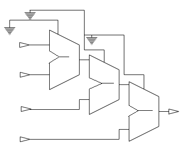
Figure1. Adders
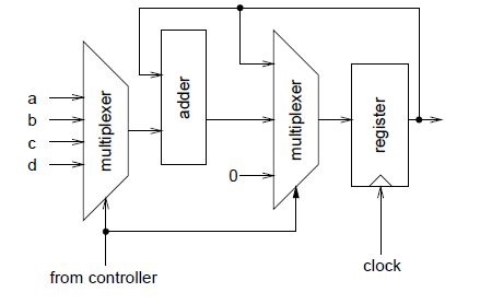
Use one adder and use it sequentially to add up all the four values. This is when we will need FSM/a control path. Let’s take a look how the circuit might look like,
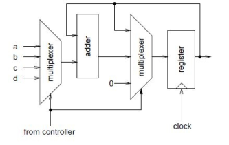
Figure2. Control path circuit
To define the data path, it works on 2-bit input sel and 1-bit inputs load and clear from the control path.
-- datapath
library ieee;
use ieee.std_logic_1164.all;
use ieee.std_logic_arith.all;
use work.averager_types.all;
entity datapath is
port (
a, b, c, d: in num;
sum: out num;
sel: in std_logic_vector (1 downto 0);
load, clear, clk: in std_logic
);
end datapath;
architecture rtl of datapath is
signal mux_out, sum_reg, next_sum_reg:num;
constant sum_zero:num:=
conv_unsigned(0, next_sum_reg’length) ;
begin
-- mux to select input to add
with sel select mux_out<=
a when "00",
b when "01",
c when "10",
d when others;
-- mux to select register input
next_sum_reg<=
sum_reg + mux_out when load = ’1’ else
sum_zero when clear = ’1’ else
sum_reg;
-- register sum
process(clk)
begin
if clk’event and clk = ’1’ then
sum_reg<= next_sum_reg;
end if;
end process;
-- entity output is register output
sum <= sum_reg;
end rtl;
The next state is the controller which controls the datapath.
-- controller
library ieee;
use ieee.std_logic_1164.all;
use work.averager_types.all;
entity controller is
port (
update in std_logic ;
sel: out std_logic_vector (1 downto 0);
load, clear: out std_logic;
clk: in std_logic
);
end controller;
architecture rtl of controller is
signal s, holdns, ns: states ;
signal tmp :std_logic_vector (3 downto 0) ;
begin
-- select next state
with s select ns <=
add_a when clr,
add_b when add_a,
add_c when add_b,
add_d when add_c,
hold when add_d,
holdns when others; -- hold
-- next state if in hold state
holdns<=
clr when update = ’1’ else
hold;
-- state register
process(clk)
begin
if clk’event and clk = ’1’ then
s <= ns;
end if;
end process;
-- controller outputs
with s select sel<=
"00" when add_a,
"01" when add_b,
"10" when add_c,
"11" when others;
load <= ’0’ when s = clr or s = hold else ’1’;
clear <= ’1’ when s = clr else ’0’;
end rtl;
Basic 4-bit adder
Simplest design: cascade full adders
- Critical path goes from Cin to Cout
- Design full adder to have fast carry delay
Critical path passes through majority gate
- Built from minority + inverter
- Eliminate inverter and use inverting full adder

Carry Look ahead adder
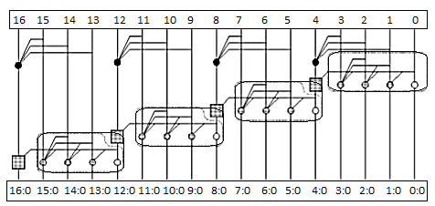
To improve the speed of addition operation, carry propagation delay of adders is important.
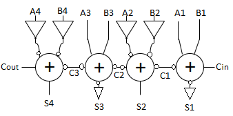
Fig 3 Look ahead carry
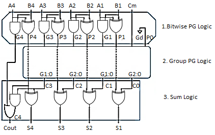
In general, a CLA using k groups of n bits each has a delay of tCLA = tpg +tpg(n)+[(n-1) + (k-1)] tAO + txor
Carry Bypass Adder

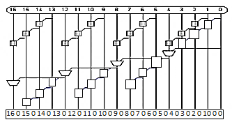
Fig 4 Carry By-pass adder
Carry select adder

Fig 5 Carry select adder
Booth Multiplier
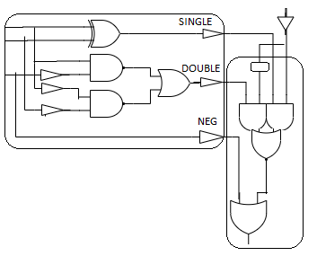
Inputs | Partial Product | Boolean series | ||||
X2l+1 | X2l | X2l-1 | PP1 | SINGLEL | DOUBLEl | NEGl |
0 | 0 | 0 | 0 | 0 | 0 | 0 |
0 | 0 | 1 | Y | 1 | 0 | 0 |
0 | 1 | 0 | Y | 1 | 0 | 0 |
0 | 1 | 1 | 2Y | 0 | 1 | 0 |
1 | 0 | 0 | -2Y | 0 | 1 | 1 |
1 | 0 | 1 | -Y | 1 | 0 | 1 |
1 | 1 | 0 | -Y | 1 | 0 | 1 |
1 | 1 | 1 | -0 (=0) | 0 | 0 | 1 |
Booth Hardware

Sign Extension
Simplified Sign Ext
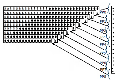
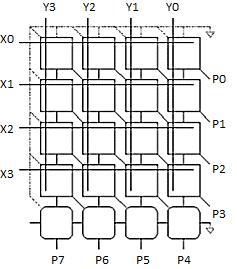
4x4 array multiplier
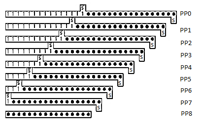
Fig 6 Array Multiplier
Rectangular Array
Squash array to fit rectangular floorplan
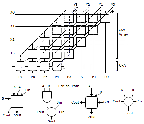
Delay calculation
Multiplier for 5 bits by 4 bits
5 X 4 array multiplier
Wallace multiplier
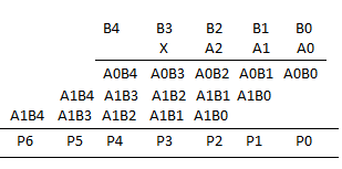
Fig 7 Wallace Multiplier
Key takeaway
A multiplication method in which an array of identical cells generates new partial product and accumulation of it at the same time. We can use pipelines at each level. The delay is logarithmically proportional to the bit size of multiplicand and multiplier if we use the high-speed array multiplier circuit.
Logical Shift: – Shifts number left or right and fills with 0’s
• 1011 LSR 1 = 0101 1011 LSL1 = 0110
Arithmetic Shift: – Shifts number left or right. Rt shift sign extends
• 1011 ASR1 = 1101 1011 ASL1 = 0110
Rotate: – Shifts number left or right and fills with lost bits
• 1011 ROR1 = 1101 1011 ROL1 = 01
Funnel Shifter
Shift Type | Z2N-2:N | ZN-1 | ZN-2:0 | Offset |
Rotate Right | AN-2:0 | AN-1 | AN-2:0 | K |
Logical Right | 0 | AN-1 | AN-2:0 | K |
Arithmetic Right | Sign | AN-1 | AN-2:0 | K |
Rotate Left | AN-1:1 | A0 | AN-1:1 |  |
Logical/ Arithmetic Left | AN-1:1 | A0 | 0 |  |
Array Funnel Shifter
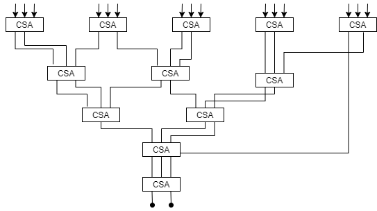
Fig 8 Array Funnel shifter
Logarithmic Funnel Shifter
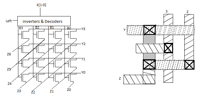
Fig 9 Log Funnel Shifter
Barrel Shifter
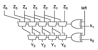
Fig 10 Barrel shifter
32-bit Logarithmic Barrel
Datapath never wider than 32 bits. First stage pre-shifts by 1 to handle left shifts.
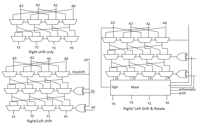
Fig 11 32-bit Log barrel
ALU’s comprise the combinational logic that implements logic operations such as AND, OR, NOT gate and arithmetic operations, such as Adder, Subtractor.
Functionally, the operation of typical ALU is represented as shown in diagram below.
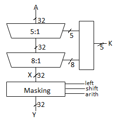
Figure 12. Functional Description of 4-bit Arithmetic Logic Unit
Controlled by the three function select inputs (sel 2 to 0), ALU can perform all the 8 possible logic operations
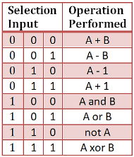
VHDL Code for 4-bit ALU
library IEEE;
use IEEE.STD_LOGIC_1164.ALL;
use IEEE.NUMERIC_STD.ALL;
entity alu is
Port ( inp_a : in signed(3 downto 0);
inp_b: in signed(3 downto 0);
sel: in STD_LOGIC_VECTOR (2 downto 0);
out_alu: out signed(3 downto 0));
end alu;
architecture Behavioral of alu is
Begin
process(inp_a, inp_b, sel)
Begin
case sel is
when "000" =>
out_alu<= inp_a + inp_b; – addition
when "001" =>
out_alu<= inp_a - inp_b; – subtraction
when "010" =>
out_alu<= inp_a - 1; – sub 1
when "011" =>
out_alu<= inp_a + 1; – add 1
when "100" =>
out_alu<= inp_a and inp_b; – AND gate
when "101" =>
out_alu<= inp_a or inp_b; – OR gate
when "110" =>
out_alu<= not inp_a; – NOT gate
when "111" =>
out_alu<= inp_a xor inp_b; – XOR gate
when others =>
NULL;
end case;
end process;
end Behavioral;
Testbench VHDL Code for 4-Bit ALU
LIBRARY ieee;
USE ieee.std_logic_1164.ALL;
USE ieee.numeric_std.ALL;
ENTITY Tb_alu IS
END Tb_alu;
ARCHITECTURE behavior OF Tb_alu IS
– Component Declaration for the Unit Under Test (UUT)
COMPONENT alu
PORT(
inp_a: IN signed(3 downto 0);
inp_b: IN signed(3 downto 0);
sel: IN std_logic_vector(2 downto 0);
out_alu: OUT signed(3 downto 0)
);
END COMPONENT;
– Inputs
signal inp_a: signed(3 downto 0) := (others => '0');
signal inp_b: signed(3 downto 0) := (others => '0');
signal sel: std_logic_vector(2 downto 0) := (others => '0');
– Outputs
signal out_alu: signed(3 downto 0);
BEGIN
– Instantiate the Unit Under Test (UUT)
uut: alu PORT MAP (
inp_a =>inp_a,
inp_b =>inp_b,
sel =>sel,
out_alu =>out_alu
);
– Stimulus process
stim_proc: process
Begin
– hold reset state for 100 ns.
wait for 100 ns;
– insert stimulus here
inp_a<= "1001";
inp_b<= "1111";
sel<= "000";
wait for 100 ns;
sel<= "001";
wait for 100 ns;
sel<= "010";
wait for 100 ns;
sel<= "011";
wait for 100 ns;
sel<= "100";
wait for 100 ns;
sel<= "101";
wait for 100 ns;
sel<= "110";
wait for 100 ns;
sel<= "111";
end process;
| |
END; | |
Simulation Result for 4-bit ALU

Figure 13. ALU
- To select right structure before starting a circuit optimization.
- Determine the critical timing path through the circuit.
- Circuit size is not only determined by the number and size of the transistors.
- An obscure optimization can sometimes help to get a better result.
- Power and speed can be traded off through a choice of circuit sizing, supply voltages and transistor threshold.
In order to fully evaluate the benefit of a serial link with respect to the parallel topology we should consider both Ag and Ec. Since the proposed scheme guarantees no performance loss, the benefits of serialization for a specific design can be easily evaluated without advanced architectural studies. Given the specifications for the power consumption, we can estimate the maximum energy per bit allowed for the intra-chip communication. Hence, for each design, the best serialization level can be chosen such that the power consumption of the vertical link does not exceed the one required by the design specifications.
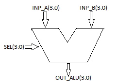
Fig 14: Ag and Ec for (a) 5µm TSVs (b) 10µm TSVs and (c) 40µm TSVs
This study can be considered as a reference for 3D -ICs architects. The graphs in Figure a, b and c depicts the area-energy trends for each TSV technology in a 2-layer system. For large TSVs the energy cost due to the serialization is almost negligible with respect to the area saved by reducing the number of TSVs. Reducing the TSV diameter we can see that Ag lowers while Ec increases. As discussed in the previous section, despite the power overhead, the energy per bit still remains low enough to consider the link as low-power. We define the energy gain as
EG = 1/Ec
The best trade-off between area and energy can be evaluated by finding the serialization level that gives the most area saved at the minimum energy cost. To the end, the product Ag xEg plotted in Figure below.
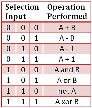
Fig 15 Area gain - energy gain product.
The best area-energy trade-off corresponds to the maximum of the Ag xEg plot. It is interesting to notice that for the TSV technologies considered, this is independent from the TSV size, with 8-bit serialization level being the optimum point.
The memory array is classified into 3 types - Random Access memory (RAM), Serial access memory and content addressable memory (CAM). We will discuss each type in detail.

Read only memory (ROM)
The basic idea of the memory that can only be read and never altered is called Read only memories. There are vast and variety of potential applications for these kinds of memories. Programs for processors with fixed applications such as washing machines, calculators and game machines, once developed and debugged, need only reading. Fixing the contents at manufacturing time leads to small and fast implementation. There are different ways to implement the logic of ROM cells, the fact that the contents of a ROM cell are permanently fixed considerably simplifies its design. The cell should be designed so that a „0‟ or „1‟ is presented to the bit line upon activation of its” wordline. The different approaches for implementing the ROM cells are Diode ROM, MOS ROM 1 and MOS ROM 2. These are the main approaches for designing a larger density ROMs.
Programmable ROM (PROM):
The technology that offers its users to program the memory one time is called Programmable ROM. It is also called as WRITE ONCE device. This is most often accomplished by introducing fuses (implemented in nichrome, polysilicon, or other conductors) in the memory cell. During the programming phase, some of these fuses are blown by applying a high current, which disables the connected transistor. While PROMs have the advantage of being “customer programmable,” the single write phase makes them unattractive. For instance, a single error in the programming process or application makes the device unstable. This explains the current preference for devices that can be programmed several times. The Floating-Gate transistor is the device at the heart of the majority of reprogrammable memories. Various attempts have made to create a device with electrically alterable characteristics and enough reliability to support a multitude of write cycles. The floating gate structure is similar to a traditional MOS device, except that an extra polysilicon strip is inserted between the gate and channel.
This strip is not connected to anything and is called a floating gate. The most obvious impact of inserting this extra gate is to double the gate oxide thickness tox, which results in a reduced device transconductance as well as an increased threshold voltage. Though these properties are not desirable but from other point of view this device acts as a normal transistor. The most important property of this device is that the threshold voltage of this device is programmable. By applying a high voltage (above 10V) between the source and the gate-drain terminals creates a high electric field and causes avalanche injection to occur.
Electrons acquire sufficient energy to become “hot” and traverse through the first oxide insulator, so that they get trapped on the floating gate. In reference to the programming mechanism, the floating-gate transistor is often called a floating-gate avalanche- injection MOS. The trapping of electrons on the floating gate effectively drops the voltage on the gate. This process is self-limiting – the negative charge accumulated on the floating gate reduces the electrical field over the oxide so that ultimately it becomes incapable of accelerating any more hot electrons. Virtually all non-volatile memories are currently based on the floating-gate mechanism. Different classes can be identified, based on the erasure mechanism.
Erasable-programmable Read-Only Memory (EPROM):
The erasure mechanism in EPROM is based on the shining ultraviolet light on the cells through a transparent window in the package. The UV radiation renders the oxide to conduct by the direct generation of electron-hole pairs in the material. The erasure process is slow depending on the UV source, it can take from seconds to several minutes. The programming takes several µs/word. Alternatively, there is another problem which exists is the limited endurance - the number of erase/program cycles is limited to a maximum of one thousand mainly as a result of UV erasing procedure. The device thresholds might vary with repeated programming cycles. The on-chip circuitry is designed in such a way that it also controls the value of the thresholds to within a specified range during programming.
The injection of large channel current of 0.5 mA at a control gate voltage of 12.5V causes high power dissipation during programming. On the other hand, EPROM is extremely simple and dense, making it possible to fabricate large memories at a low cost. Therefore, EPROMs were attractive in applications that do not require reprogramming. The major disadvantage of the EPROM is that the erasure procedure has to occur “off system”. This means the memory must be removed from the board and placed in an EPROM programmer for programming.
Electrically Erasable Programmable Read-Only Memory EEPROM)
The disadvantage of the EPROM [16] is solved by using a method to inject or remove charges from a floating-gate namely – tunneling. A modified floating-gate device called FLOTOX (floating-gate tunneling oxide) transistor is used as programmable device that supports an electrical-erasure procedure. It resembles FAMOS (floating-gate avalanche MOS) device, except that a portion of the dielectric separating the floating gate from the channel and drain is reduced in thickness to about 10 nm or less.
The main advantage of this programming approach is that it is reversible; that is, erasing is simply achieved by reversing the voltage applied during the writing process. The electrons injection on floating-gate raises the threshold, while the reverse operation lowers the VT. When a voltage of approximately 10V (equivalent to 109 V/m) is applied over the thin insulator, electrons travel to and from the floating gate through a mechanism called Fowler – Nordheim tunneling.
Flash Electrically Erasable Programmable ROM (Flash):
The concept of Flash EEPROMs is a combination of density of EPROM with versatility of EEPROM structures, with cost and functionality ranging from somewhere between two. Most Flash EEPROM devices use the avalanche hot-electron-injection approach to program the device. Erasure is performed using Fowler – Nordheim tunneling, as from EEPROM cells. The main difference is that erasure procedure is performed in bulk for a complete chip or for the subsection of the memory. Erasing complete memory core at once makes it possible to carefully monitor of the device characteristics during erasure.
The monitoring control hardware on the memory chip regularly checks the value of the threshold during erasure, and adjusts the erasure time dynamically. This approach is only practical when erasing large chunks of memory at a time; hence the flash concept. One of the many existing alternatives for Flash EEPROMs memories are ETOX devices. It resembles a FAMOS gate except that a very thin tunneling gate oxide is utilized (10 nm). Different areas of the gate oxide are used for programming and erasure. Programming is performed by applying a high voltage (12V) on the gate and drain terminals for a grounded source, while erasure occurs with the gate rounded and the source at 12V.
The Programming cycle starts with an erase operation. In erase operation, A 0V gate voltage is applied and a 12V supply is given at source. Electrons, if any, are ejected to the source by tunneling. All cells are erased simultaneously. The variations caused in the threshold voltage at the end of erase operation are due to different initial values of cell threshold voltage and variations in oxide thickness. This can be solved in two methods: 1.
The array cells are programmed before applying the erase pulse so that the entire threshold starts at approximately same time. 2. An erase pulse of controlled width is applied. Subsequently the whole array is read to ensure that all the cells are erased. If not, another erase pulse is applied followed by the read cycle. For write (programming) operation, a high voltage is applied to the gate of the selected device. If a „1‟ is applied to the drain at that time, hot electrons are generated and injected onto the floating gate, raising the threshold. Read operation corresponds as the wordline is raised to 5V; it causes a conditional discharge of bitline.
Random Access memory (RAM):
Random access memory is a type of computer data storage. It is made of integrated circuits that allow the stored data to be accessed in any order i.e., at random and without the physical movement of storage medium or a physical reading head. RAM is a volatile memory as the information or the instructions stored in the memory will be lost if the power is switched off. The word “random” refers to the fact that any piece of data can be returned at a constant time regardless of its physical location and whether or not it is related to the previous piece of data.
This contrasts with the physical movement devices such as tapes, magnetic disks and optical disks, which rely on physical movement of the recording medium or reading head. In these devices, the retrieval time varies with the physical location and the movement time takes longer than the data transfer. The main advantages of RAM over types of storage which require physical movement is that retrieval times are short and consistent. Short because no physical movement is necessary and consistent the time taken to retrieve the data does not depend on the current distance from a physical head. The access time for retrieving any piece of data in RAM chip is same.
The disadvantages are its cost compared to the physical moving media and loss of data when power is turned off RAM is used as 'main memory' or primary storage because of its speed and consistency. The working area used for loading, displaying and manipulating applications and data. In most personal computers, the RAM is not an integral part of the motherboard or CPU. It comes in the easily upgraded form of modules called memory sticks. These can quickly be removed and replaced when they are damaged or when the system needs up gradation of memory depending on current purposes. A smaller amount of random- access memory is also integrated with the CPU, but this is usually referred to as "cache" memory, rather than RAM. Modern RAM generally stores a bit of data as either a charge in a capacitor, as in dynamic RAM, or the state of a flip-flop, as in static RAM.
Static Random Access Memory (SRAM)
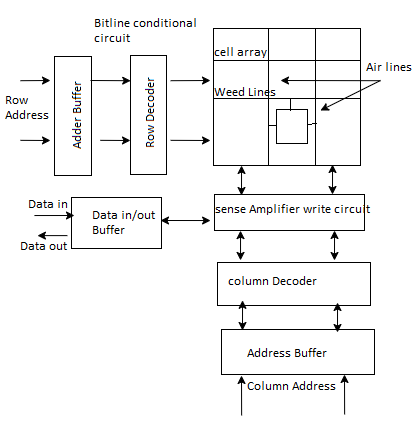
The typical SRAM design is shown in figure the memory array contains the memory cells which are readable and writable. The Row decoder selects from 1 out of n = 2k rows, while the column decoder selects l = 2i out of m = 2j columns. The addresses are not multiplexed as it in the DRAM. Sense amplifier detects small voltage variations on the memory complimentary bitline which reduces the reading time. The conditioning circuit is used to pre-charge the bitlines.
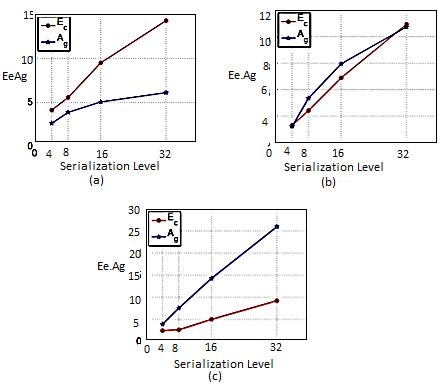
Fig 14 SRAM Architecture
In a read operation, the bitlines are precharged to some reference voltage usually close to the supply voltage. When word line turns high, the access transistor connected to the node storing „0‟ starts discharging the bitline while the complementary bitline remains in its precharged state, resulting in a differential voltage between the bitline pair. Since the SRAM has an optimized area results in a small cell current and slow bitline discharge rate. In order to speed up the RAM access, sense amplifiers are used which amplify the small bitline signal and eventually drive it to the external world.
The word “static” means that the memory retains its contents as long as the power is turned on. Random access means that locations in the memory can be written to or read from in any order, regardless of the memory location that was last accessed. Each bit in an SRAM is stored on four transistors that form two cross-coupled inverters. This storage cell has two stable states which are used to denote „0‟ and „1‟.
The access transistors are used to access the stored bits in the SRAM during read or write mode. It thus typically takes six MOSFETs to store one memory bit. Access to the cell is enabled by the word line WL which controls the two access transistors N1 and N2 which, in turn, control whether the cell should be connected to the bitlines BL and /BL. They are used to transfer data for both read and write operations.
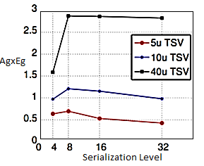
Fig 15 A logic diagram of a CMOS static memory cell
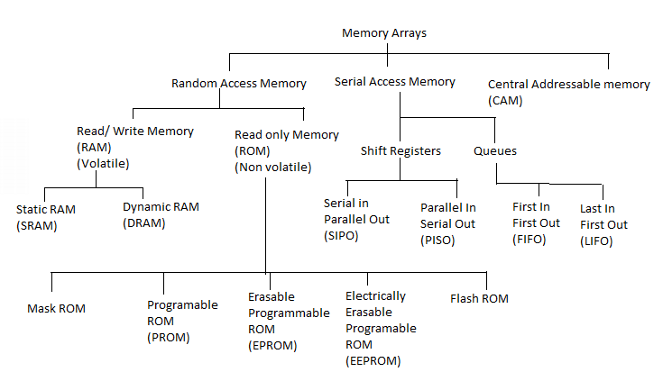
Fig 16 A schematic of a CMOS static memory cell
Principles of operations
In order to consider operation of the static read/write memory we have to take into account: Relatively large parasitic column capacitances, CC and Cc
Column pull-up pMOS transistors, as shown in Figure
A CMOS static memory cell with column pull-up transistors and parasitic column capacitances
When none of the word lines is selected, that is, all S signals are ‘0’, the pass transistors n3, n4 are turned off and the data is retained in all memory cells. The column capacitances are charged by the drain currents of the pull-up pMOS transistors, p3, p4. The column voltages VC and V c¯ both reach the level just below VDD − VT p, say 3.5V for VDD = 5V and the threshold voltage VT p = 1V.
For the read or write operations we select the cell asserting the word line signal S= ‘1’. For the write operation we apply a low voltage to one of the bit line, holding the other one high. To write ‘0’ in the cell, the column voltage VC is forced to low (C = 0). This low voltage acts through a related pass transistor (n3) on the gates of the corresponding inverter (n2, p2) so that its input goes high. This sets the signal at the other inverter Q = 0. Similarly, to write ‘1’ in the cell, the opposite column voltage VC¯ is forced to low (C¯ = 0) which sets the signal Q = 1.
During the read ‘1’ operation, when the stored bit is Q = 1, transistors n3, p1 and n4, n2 are turned on. This maintains the column voltage VC at its steady state high level (say 3.5V) while the opposite column voltage VC¯ is being pulled down discharging the column capacitance CC¯ through transistors n4, n2 so that VC > VC¯. Similarly, during the read ‘0’ operation we have VC < VC¯. The difference between the column voltages is small, say 0.5V, and must be detected by the sense amplifiers from data-read circuitry.
Key takeaway
Random access memory is a type of computer data storage. It is made of integrated circuits that allow the stored data to be accessed in any order i.e., at random and without the physical movement of storage medium or a physical reading head.
EEPROM The main advantage of this programming approach is that it is reversible; that is, erasing is simply achieved by reversing the voltage applied during the writing process. The electrons injection on floating-gate raises the threshold, while the reverse operation lowers the VT.
SRAM Read Circuitry
The structure of the read circuitry is shown in Figure
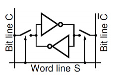
Fig 17 The structure of the write circuitry associated with one column of the memory cells. During the read operation the voltage level on one of the bit lines drops slightly after the pass transistors in the memory cell are turned on.
The read circuitry consists of two-level sense amplifiers:
• One simple cross-coupled sense amplifier per column of memory cells,
• One current-mirror differential sense amplifier per the memory chip.
The cross-coupled sense amplifier works as a latch. Assume that the voltage on the bit line C start to drop slightly when the memory access pass transistors are activated by the word line signal S, and that the clk signal is high so that the transistor M3 is turned on. Now, higher voltage on the gate of M1 transistor than on the gate of M2 starts the latching operation which pulls the VC voltage further down switching the transistor M2 off.
As a result, the parasitic capacitance, CC is discharged through M1 and M3. In this way a small difference between column voltages is amplified. The amplified (discriminated) column voltages are passed through transistors M4 and M5 to the main sense amplifier. The schematic of a typical differential current-mirror sense amplifier is shown in Figure
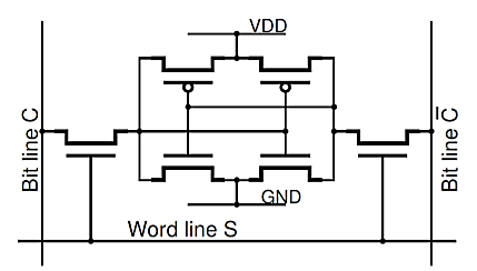
Fig 18 A CMOS differential current-mirror sense amplifier
Dynamic Read-Write Memory (DRAM)
In the static CMOS read-write memory data is stored in six-transistor cells. Such a memory is fast and consumed small amount of static power. The only problem is that a SRAM cell occupies a significant amount of silicon space. This problem is addressed in the dynamic read-write memory (DRAM). In a dynamic RAM binary data is stored as charge in a capacitor. The memory cell consists of a storage capacitor and an access transistor as shown in Figure
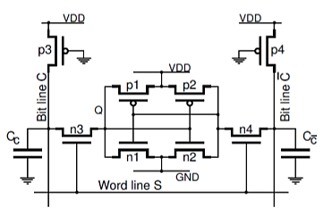
Fig 19 A one-transistor DRAM memory cell
Data stored as charge in a capacitor can be retained only for a limited time due to the leakage current which eventually removes or modifies the charge. Therefore, all dynamic memory cells require a periodic refreshing of the stored data before unwanted stored charge modifications occur. Typical storage capacitance has a value of 20 to 50 Ff. Assuming that the voltage on the fully charged storage capacitor is V = 2.5V, and that the leakage current is I = 40pA
The DRAM cell occupies much smaller silicon area than the SRAM cell. The size of a DRAM cell is in the order of 8F2, where F is the smallest feature size in a given technology. For F = 0.2μm the size is 0.32μm2
• No static power is dissipated for storing charge in a capacitance. The storage capacitance CS, which is connected between the drain of the access transistor (the storage node) and the ground, is formed as a trench or stacked Capacitor. The stacked capacitor is created between a second polysilicon layer and a metal plate covering the whole array area. The plate is effectively connected to the ground terminal. To consider read/write operations we have to take into account a significant parasitic capacitance CC associated with each column, as shown in Figure
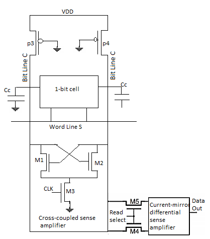
Fig 19 A single SRAM cells with a column capacitance shown
Typically, before any operation is performed each column capacitance b is precharged high. The cell is selected for a read/write operation by asserting its word line high (S = 1). This connects the storage capacitance to the bit line. The write operation is performed by applying either high or low voltage to the bit line thus charging (write ‘1’) or discharging (write ‘0’) the storage capacitance through the access transistor. During read operation there is a flow of charges between the storage capacitance C1 and the column capacitance, CC.
As a result, the column voltage either increases (read ‘1’) or decreases (read ‘0’) slightly. This difference can then be amplified by the sense amplifier. Note that the read operation destroys the charge stored on the storage capacitance C1 (“destructive readout”). Therefore, the data must be restored (refreshed) each time the read operation is performed.
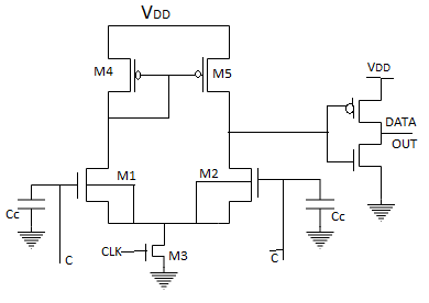
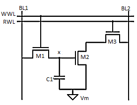
Fig 20 Three Transistor Dynamic RAM
The write operation performed is shown for three transistor Dynamic RAM (Figure 1.2) as the appropriate data value is written on BL1 and asserting the write-wordline (WWL). The data is retained as charge on capacitance Cs once WWL is lowered. When reading the cell, the readwordline (RWL) is raised. The storage transistor M2 is either on or off depending upon the stored value. The bitline BL2 is precharged to VDD before performing read operation. The series connection of M2 and M3 pulls BL2 low when a “1” is stored. BL2 remains high in the opposite case. The cell is inverting; that is, the inverse value of the stored signal is sensed on the bitline.
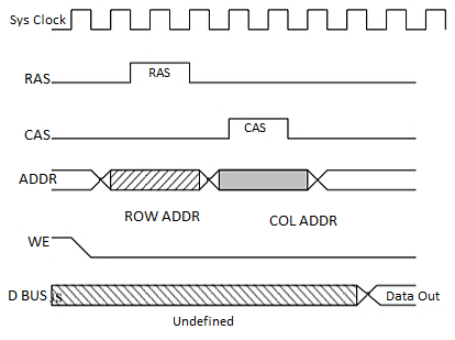
DRAM Timing:
DRAM module is asynchronous, Timing depends on how long it takes to respond to each operation.
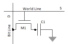
Fig 21 Timing Diagram
DRAM cannot be read as fast (or as easy) as SRAM.
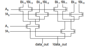
The peripheral memory circuitry consists of
Row Decoders
Collection of 2M complex logic gates organized in a regular, dense fashion
(N)AND decoder for 8 address bits
WL (0) =! A7 &! A6 &! A5 &! A4 &! A3 &! A2 &! A1 &! A0
WL (255) = A7 & A6 & A5 & A4 & A3 & A2 & A1 & A0
NOR decoder for 8 address bits
WL (0) =! (A7 | A6 | A5 | A4 | A3 | A2 | A1 | A0)
WL (255) =! (! A7 |! A6 |! A5 |! A4 |! A3 |! A2 |! A1 |! A0)
Implementing a Wide NOR Function
Single stage 8x256 bit decode
One 8 input NOR gate per row x 256 rows = 256 x (8+8) = 4,096
Pitch match and speed/power issues
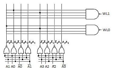
Decompose logic into multiple levels
! WL (0) =! (! (A 7 | A 6) &! (A 5 | A 4) &! (A 3 | A 2) &! (A1 | A 0))
First level is the predecoder (for each pair of address bits, form Ai|Ai-1, Ai|! Ai-1, Ai|Ai-1, and! Ai|! Ai-1) Sp11 CMPEN 411 L24 S.8 i i-1 i i-1 i i-1 i i-1
Second level is the word line driver
Predecoders reduce the number of transistors required Four sets of four 2-bit NOR predecoders = 4 x 4 x (2+2) = 64
256-word line drivers, each a four input NAND – 256 x (4+4) = 2,048 - 4,096 vs 2,112 = almost a 50% savings
Number of inputs to the gates driving the WLs is halved, so the propagation delay is reduced by a factor of ~4
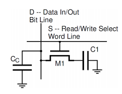
Fig NAND decoder using 2-input pre input pre-decoders
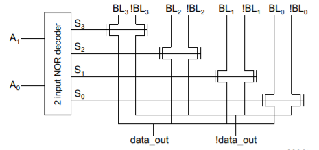
Pass Transistor Based Column Decoder
Tree Based Column Decoder
Bit Line Precharge Logic
Sense Amplifiers
Amplification – resolves data with small bit line swings (in some DRAMs required for proper functionality)
Delay reduction – compensates for the limited drive capability of the memory cell to accelerate BL transition
Power reduction – eliminates a large part of the power dissipation due to charging and discharging bit lines
Signal restoration – for DRAMs, need to drive the bit lines full swing after sensing (read) to do data refresh
Approaches to Memory Timing
Key takeaway
Decoder complexity comparison
Conf. | Data/Row | Row Decoder | Column Decoder |
1D | 8b | 10b = a 10x210 decoder single stage = 20,480 Two stage = 10.320 |
|
2D | 32b (32x256 core) | 8b=8x28 decoder Single stage = 4,096 T Two stage = 2,112T | 2b = 2x22 decoder PT=76 T Tree=96 T |
2D | 64b (64x128 core) | 7b=7x27 decoder Single stage=1,792 T Two Stage = 1,072 T | 3b = 3x23 decoder PT = 160 T Tree = 224 T |
2D | 128b (128x64 core) | 6b = 6x26 decoder Single Stage = 768T Two stage = 432 T | 4b = 4x24 decoder PT = 336 T Tree = 480 T |
References:
1. D.A. Pucknell, K. Eshraghian, ‘Basic VLSI Design’, 3rd Edition, Prentice Hall of India, New Delhi,
2003.
2. Debprasad Das, VLSI Design, Oxford University Press, 2010.
3. Eugene D. Fabricius, ‘Introduction to VLSI Design’, Tata McGraw Hill, 1990.