MODULE 8
INTRODUCTION TO SOLIDS AND SEMICONDUCTORS
Metals form a unique type of bond known as a metal bond and form the lattice structure.
The uniqueness of this type of bonding mode lies in the fact that, unlike the ionic bond and the covalent bond in which the electron distribution is between two atoms and the electrons remain localized, in the metallic bond the bond is formed among all the atoms in the network and the free electrons of each atom are shared by the entire network.
These free electrons move freely through the network and are therefore called electron gas.
Neglecting the electron-electron interaction and the electron-ion interaction, the electrons seem to move in a box confined to a periodic collision with ions in the network.
Drude gave this idea and used it to successfully explain many properties of metal, such as electrical conductivity, thermal conductivity, etc.
Drude applied simple mechanical equations to electrons to derive different expressions and also to arrive at Ohm's law.
Normally, the electrons have random movement throughout the network, mainly due to thermal energy, and the average net effect is zero.
However, when the electric field is applied to the metal, another component of velocity is superimposed on each electron due to the force acting on it by virtue of its charge.
According to Newtonian mechanics we can write

Where, e= charge on electron,
E = applied electric field in V/m
m = mass of electron
x = distance in the direction of motion.
Integrating equation (i)

Where, A and C are constants.
Equation (ii) is the calculation of velocity of electrons, henceforth C has measurement of velocity, and can simply be arbitrary velocity of electron which it had at the early stage when no field was applied.
Henceforth,
Though, as we discussed prior this random velocity medians out to zero, thus the average velocity of the electrons can be transcribed as-

The equation above indicates that the speed continues to increase indefinitely with time until E is turned on, however this is not possible.
The explanation is given by saying that the electrons do not move freely in the network, but they collide with the ions present in the network structure, lose their speed and again accelerate and collide again, etc.
So, considering the average effect, we believe that, on average, the time between two collisions is T, known as the relaxation time or collision time, and the average speed reached by the electrons in the time period T is known as the velocity of drift.

- Now, for number of electrons per unit volume as n, the quantity of charge passing done a cross section A in time dt will be assumed by

Henceforth the current curving will be given by,

And hereafter the current density determination be,

Placing the value of drift velocity after equations (iv) in (v),

Which is nothing but the Ohm’s Lawhimself, wherever,

Now here we describe a new term recognized as mobility, definite as drift velocity per unit electric field,

Its unit is
We also detect from the appearance of conductivity that

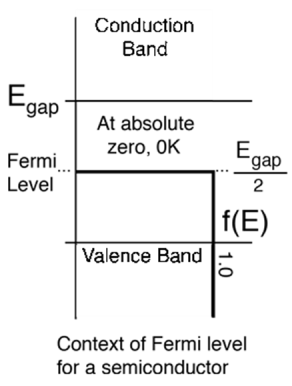
Fermi level "is the term used to describe the top of the collection of electronic energy levels at absolute zero temperature.
- This concept is derived from Fermi-Dirac statistics. Electrons are fermions and according to the principle of exclusion of Pauli cannot exist in identical energy states. So absolute zero accumulates in the lowest available energy states and builds a "Fermi sea" of electron energy states.
- The Fermi level is the surface of that sea in absolute zero where no electron will have enough energy to rise above the surface.
- Fermi energy is a concept of fundamental importance for understanding the electrical and thermal properties of solids.
- Both electrical and normal thermal processes involve energies of a small fraction of volts of electrons.
- But the energies of the Fermi metals are in the order of the electron volt
- This implies that the vast day mag of the electrons cannot receive energy from those processes because there was no energy available for them to enter w within a fraction of electron volts of their current energy.
- Limited to a small depth of energy, these interactions are limited to "waves in the Fermi Sea."
- At higher temperatures, there will be a certain fraction, characterized by the Fermi function, above the Fermi level.
- The Fermi level plays an important role in solid band theory. In p-type and n-type doped semiconductors, the Fermi level is displaced by impurities, illustrated by their band gaps.
- The Fermi level is indicated as an electronic chemical potential in other contexts.
- In metals, the Fermi energy provides us with information about the speeds of the electrons that participate in normal electrical conduction.
- The amount of energy that can be given to an electron in these conduction processes is of the order of volts of microelectrons (see example of copper wire), therefore, only those electrons very close to Fermi energy can participate.
- The Fermi velocity of these conduction electrons can be calculated from the Fermi energy.

This speed is a portion of the microscopic Ohm's Law for electrical conduction.
For a metal, the density of conduction electrons can be implicit from the Fermi energy
Fermi energy also shows a significant role in kind the unidentified of why electrons do not contribute meaningfully to the specific heat of solids at normal temperatures, while dominatingly contribute to thermal conductivity and electrical conductivity.
Since only a small fraction of the electrons in a metal are within the thermal energy kT of the Fermi energy, they are "frozen" by the heat capacity of the Pauli principle. At very low temperatures, the specific heat of the electron becomes significant.
The density of states (DOS) is fundamentally the number of dissimilar states at a specific energy level that electrons are allowable to occupy, i.e. the amount of electron states for each unit volume for each unit energy.
Majoritythings such as specific heat, paramagnetic susceptibility and additional transport singularities of conductive solids depend on this meaning.
DOS calculations agree one to regulate the general supply of states as a function of energy and can also govern the spacing amid energy bands in semi-conductors.
Density of States for Waves
Before we get involved in the derivation of the DOS of electrons in a material, it may be easier to first consider just an elastic wave propagating through a solid.
Elastic waves are in orientation to the lattice vibrations of a solid included of distinct atoms. However, when the wavelength is very long, the atomic nature of the solid can be unnoticed and we can treat the material as a constant medium.
We startby the 1-D wave calculation:
With which we then have a answer for a propagating plane wave: (1)
(1)
q= wave number ,
,
A=amplitude,
ω = frequency,
Vs = velocity of sound
Dispersion Relation:

In equation (1), the activist factor,  can be absent because it is not relevant to the derivation of the DOS [2].
So now we will use the answer: (2)
(2)
To start, we must apply some type of boundary circumstances to the organization.
The easiest way to do this is to reflect a periodic boundary circumstance.
Through a periodic limitcondition, we can visualize our system requiring two ends, one being the origin 0 and the other L.
We now say that the origin end is unnatural in a way that it is always at the similar state of oscillation as end L [2].
This boundary state is signified as:
Now we relate the boundary state to equation (2) to acquire:
Now, spending Euler’s individuality;  we can see that there are firm values of qL which fulfil the above equation.
Those standards are  for any integer, n. Leaving the relation:
If you choose integer standards for n and design them along an axis q you get a 1-D line of points, known as modes, with a spacing of  amid each mode.
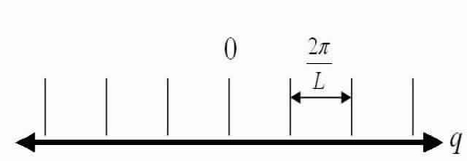

We now have that the number of modes in an interval dq in q-space equals:

By means of the dispersion relation we can find the number of modes inside a frequency range dω that lies inside .
.
This number of modes in that range is signified byg(ω)dω , where gω is demarcated as the density of states.
So now we get that g(ω)dω = which
which
We go into:
We do so in order to practice the relation:
And
Get:
we grow by a factor of two since there are modes in positive and negative q-space, and we acquire the density of states for a phonon in 1-D:

2-D:
We can now originate the density of states for two dimensions.
Equation (2) becomes: now apply the same boundary circumstances as in the 1-D case:

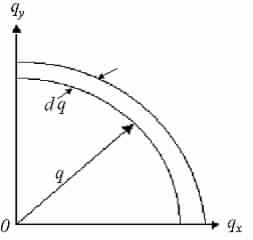
We now study an area for each point in q-space =(2π/L)2 and discovery the number of modes that lie inside a flat ring with thickness dq, a radius q and area:
Number of modes inside intermission:
Now explanation for transverse and longitudinal modes (multiply by a factor of 2) and set equivalent to g(ω)dω
We get  and
and
Apply dispersal
Relation to get  which make
Simpler to the 2-D result:

3-D:
We can now derive the density of states for three dimensions.
Equation(2) develops:
Now apply the same boundary conditions as in the 1-D case to become:

We now study a volume for to each point in q-space =(2π/L)3 and discovery the number of modes that lie within a spherical shell, thickness dq, with a radius q and volume:4/3πq3
Number of modes inside shell:
Supposing a common velocity for transverse and longitudinal waves we can explanation for one longitudinal and two transverse modes for each value of q (multiply by a factor of 3) and set equal to g(ω)dω:
Apply dispersalrelative and let L3=V to get  and shorten for the 3-D result:

Bloch's Theorem
Until now, approaches to quantum mechanics to solve the problem of many bodies have been discussed.
However, the correlated nature of the electrons within a solid is not the only obstacle to solving the Schrödinger equation for a condensed matter system: for solids, the really infinite number of electrons within the solid must also be taken into account
Bloch's theorem can be used to advance in solving the last problem. Instead of having to consider an infinite number of electrons, it is necessary to consider only the number of electrons within the unit cell (or half of this number if the electrons are spin degenerate).
Bloch's theorem states that the wave function of an electron within a perfectly periodic potential can be written as

Where  is a function that keeps the periodicity of the
Potential, i.e.  , where
  is the length of the unit cell. In i is the band index, and
  is a wavevector kept to the first Brillouin Region. Meanwhile
  is a periodic function, we may enlarge it in terms of a Fourier sequence:

Where they  are mutual lattice vectors defined through
  , where m is an integer,
  is a real space lattice vector and the
  are plane wave development coefficients.
The electron wavefunctions may so be written as a linear mixture of plane waves:

Since each electron occupies a defined state, the infinite number of electrons within the solid generates an infinite number of k points. At each point k, only a finite number of available energy levels will be occupied.
Therefore, it is sufficient to consider a finite number of electrons at an infinite number of points k.
This may appear to replace one infinity (number of electrons) with another (number of k points) with a discrete advantage.
However, it is not necessary to consider all these k points; rather, since the wave functions of the electron will be almost identical for values close enough, one can represent the wave functions in a region of reciprocal space by considering the wave function at a single point k.
Therefore, it is sufficient to consider the electronic states at a finite number of points k to determine the solid-state density of the solid.
The net effect of Bloch's theorem was, therefore, to change the problem of an infinite number of electrons into one to consider only the number of electrons in the unit cell (or half of that number, depending on whether the states are degenerate by rotation or less) to a finite number of k points chosen to adequately sample the Brillouin area; This problem returns later.
The Kronig-Penney model is a shortened model for an electron in a one-dimensional periodic possible. The imaginable states that the electron can inhabit are firm by the Schrödinger equation,

In the case of the Kroning-Penney model, the potential V(x) is a periodic square wave.
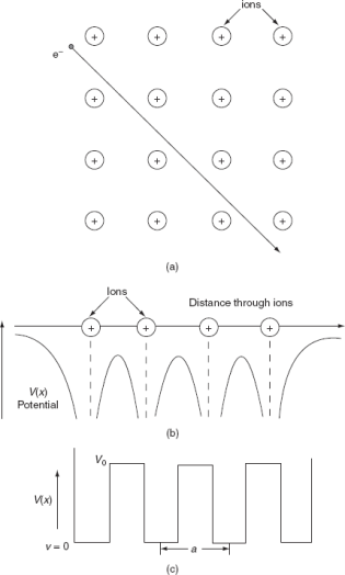
A feature of this model is that it is thinkable to systematically control the energy eigenvalues and eigenfunctions. It is also likely to discovery analytic terms for the diffusion relation (E vs. k) and the electron density of states.
The energies of the electrons can be known by solving the Schrödinger wave equation in this network. Schrödinger's time independent wave equation for the motion of an electron along the X direction is given by:
 ...............(1)
The electron energies and wave functions associated with this model can be calculated by solving the time-independent one-dimensional Schrödinger wave equations for the two regions I and II, as shown in Fig. Schrödinger's equations are: for 0<x<a.............(2)
 for -b<x<0.............(3)
We define two real quantities (say) α and β such that:

Hence, Equations (5.41) and (5.42) becomes:
 for 0<x<a
 for -b<x<0
According to Bloch's theorem, the solution of the wave function of the Schrödinger equation when the potential is periodic and to make sure that the function u (x) is also continuous and regular, can be written as:

Where u(x) is a periodic function which fulfills u(x + a) = u(x).
Using Bloch theorem and all the peripherycircumstances for the stability of the wave meaning the answer of Schrodinger wave equation got as

Where,

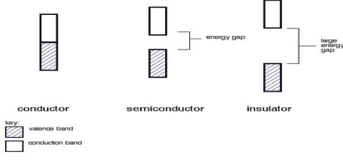
A. Conductors Metals are conductive. There is no gap between their value and the conduction bands as they overlap. There is a continuous availability of electrons in these nearby orbitals.
B. Insulators in insulators, the band gap between the valence band and the conduction band is so large that electrons cannot burst energy from the valence band to the conduction band.
C. Semiconductors have a minor energy gap amid the valence band and the conduction band. Electrons can jump into the conduction band, but not as easily as conductors do.
There are two different types of semiconductors: intrinsic and extrinsic. ME. Intrinsic Semiconductors An intrinsic semiconductor is a pure semiconductor.
For each electron that jumps into the conduction band, the missing electron will generate a hole that can move freely in the valence band. The number of holes will be equal to the number of electrons that have jumped. 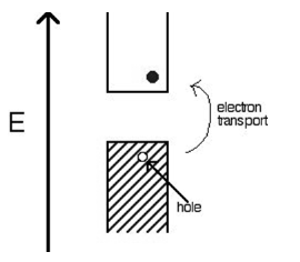
Extrinsic Semiconductors
In extrinsic semiconductors, the gap between bands is controlled by intentionally adding small impurities to the material. This process is called doping.
Doping or the addition of impurities to the network can change the electrical conductivity of the network and therefore vary the efficiency of the semiconductor.
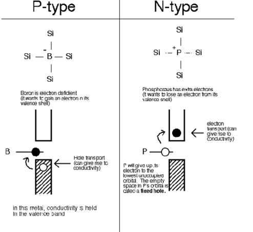
In extrinsic semiconductors, the number of holes will not be equal to the number of omitted electrons. There are two different types of extrinsic semiconductors, p-type (positively charged doping) and n-type (negativelycharged doping).
Semiconductors that are chemically pure, in other words, free of impurities are called intrinsic semiconductors. The number of holes and electrons is therefore determined by the properties of the material itself rather than impurities. In instrinsic semiconductors, the number of excited electrons is equivalent to the number of holes; n = p. They are also called non-doped semiconductors or type I semiconductors. Silicon and germanium are examples of type I semiconductors. These elements belong to the IV group of the periodic table and their atomic numbers are 14 and 32 respectively.
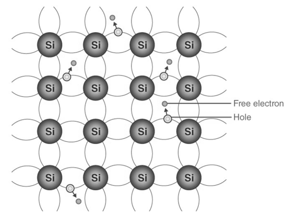
Electrons and Holes configuration in a Silicon atom
Working Mechanism of Intrinsic Semiconductors
Electronic Configuration of Silicon and Germanium
Silicon 1s2 2s22p6 3s2 3p2
Germanium 1s2 2s2 2p6 3s2 3p6 4s2 3d10 4p2
We note from the electronic configurations of both elements that have four electrons in their outermost shell or valence shell. As the temperature of the semiconductors increases, the electrons acquire more thermal energy and are released from its shell. The ionization process of the atoms in the crystal lattice creates a space in the bond between the atoms. The position from which the electron is detached has a hole equivalent to an effective positive charge. The hole is occupied by a free electron, as a result of which the last free position becomes a hole and the first free position becomes a neutral position. In this way, the hole or the actual positive charge is transferred from one position to another. In an intrinsic semiconductor, the number of free electrons is equal to the number of holes. Mathematically,
Here, ni gives the number of total concentration of intrinsic carriers which is equal to the total number of holes or the total number of electrons.
When the temperature of an intrinsic semiconductor is T = 0K, it acts alike an insulator. When the temperature increases , (T> 0), the electrons are excited and transfer from the valence band to the conduction band. These electrons partially occupy the conduction band, leaving a corresponding number of holes in the valence band.
Definition:When a semiconductor is in Thermal equilibrium, the supply function of the electrons at the energy level of E is presented by a Fermi –Dirac delivery function.
- In this case the Fermi level is defined as the level in which the probability of work of electron at that energy is ½.
- In thermal equipoise, there is no need to distinguish between conduction band quasi-Fermi level and valence band quasi-Fermi level as they are simply equivalent to the Fermi level.
- The electron in conduction band which is in equilibrium is given by
ne = Neffe · exp – | EC – EF kT |
- The holes in valance band which is in symmetry is given by
nh = Neffh · exp – | EF – EV kT |
- Balance means -holes and electron are equal in band this resources fermi energy is same or equal for both bands
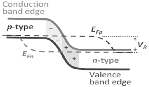
- Now for the equation of Fermi we must write down f(E, EFe, T) or f(E, EFh, T) instead of f(E,Ef,T) or E f
.
- The carrier concentration of electron or holes in conduction or valance band are as follow
ne = Neffe · [fe in C (E, EFe, T)]Neffe · exp - 
- The carrier concentration of electron or holes in conduction or valance band are as follow
ne = Neffn · [fn in C(E, EFn, T)]Neffn · exp - 
- This can be cured easily by simply setting 1 – f (E, EFh, T) =: fh in V(E, EFh, T) with fh in V existence the probability of finding holes on the available states in the valence band.
- Formally, the electron density in the valence band (EV) then contains 1 – fh in V and so on.
Diffusion
when there is a focus gradient, material will change in the direction of the highest rate of reduction of the gradient.
![\includegraphics[width=0.65\textwidth]{conc-grad.eps}](https://glossaread-contain.s3.ap-south-1.amazonaws.com/epub/1643209518_2599533.png)
Figure : Movement of material down a concentration gradient.
Drift
When an electric field is applied to a semiconductor, the carriers will move at a velocity that is relative to the magnitude of the field. This velocity is called the drift velocity vd.

Here  is called the mobility, with units
![\begin{displaymath}[\mu]= L^2V^{-1}T^{-1}.
\end{displaymath}](https://glossaread-contain.s3.ap-south-1.amazonaws.com/epub/1643209518_4236228.png)
And  is the electric field. This establishes a drift current

At symmetry, the drift and diffusion currents are equivalent.

So

![\includegraphics[width=0.65\textwidth]{drift.eps}](https://glossaread-contain.s3.ap-south-1.amazonaws.com/epub/1643209518_7411098.png)
Figure : Equilibrium condition for drift and diffusion currents.
We may write the electric field as the gradient of the potential

So

Thus

This differential equation has the solution

For the electron scattering per unit volume. But because this non-uniform electron scattering has to be kept against the potential using thermal energy, we have

We so find the Einstein relations


That is, we can express the diffusion coefficient as

a consequence which we will soon use.
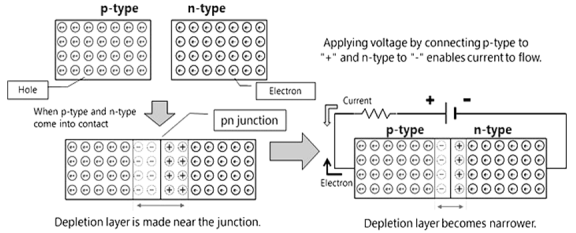
Definition: A p-n junction is an interface or a boundary between two semiconductor material types, namely the p-type and the n-type, inside a semiconductor.
- p type semiconductor have hole as majority carrier while minority carrier electron
- Similarly n type have majority electron and minority carrier hole
- When p-type and n-type come into contact depletion layer is made near the junction.
- Connecting battery positive terminal at p type and n type then we can get narrower depletion layer this kind of bias is know as forward bias while after changing terminal we can get reverse bias.
- Flow of electron and current are opposite to each other.
Reference:
1. G. MAIN, “VIBRATIONS AND WAVES IN PHYSICS”, CAMBRIDGE UNIVERSITY PRESS,1993.
2. H. J. PAIN, “THE PHYSICS OF VIBRATIONS AND WAVES”, WILEY, 2006.
3. E. HECHT, “OPTICS”, PEARSON EDUCATION, 2008.
4. A. GHATAK, “OPTICS”, MCGRAW HILL EDUCATION, 2012.
5. O. SVELTO, “PRINCIPLES OF LASERS”, SPRINGER SCIENCE & BUSINESS MEDIA, 2010.