Unit 4
Special ICs
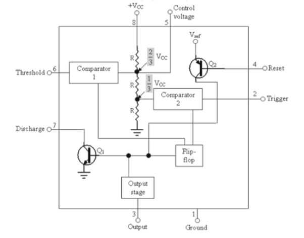
The above figure consists of three 5k internal resistors which act as voltage divider providing bias voltage of 2/3 Vcc to the upper comparator & 1/3 Vcc to the lower comparator.
It is possible to vary time electronically by applying a modulation voltage to the control voltage input terminal (5).
In the Stable state: The output of the control FF is high. This means that the output is low because of power amplifier which is basically an inverter.
Q = 1; Output = 0
At the Negative going trigger pulse: The trigger passes through (Vcc/3) the output of the lower comparator goes high & sets the FF. Q = 1; Q = 0
At the Positive going trigger pulse: It passes through 2/3Vcc, the output of the upper comparator goes high and resets the FF. Q = 0; Q = 1 The reset input (pin 4) provides a mechanism to reset the FF in a manner which overrides the effect of any instruction coming to FF from lower comparator.
Characteristics:
Monostable operation:
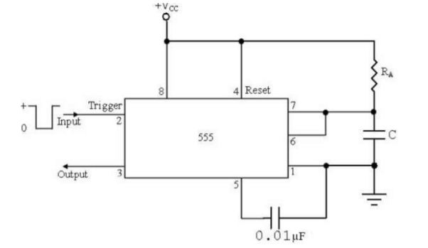
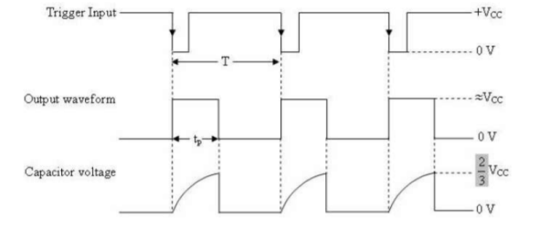
When the output is low the circuit is in a stable state, transistor Q1 is ON & capacitor C is shorted to ground. The output remains low.
During negative going trigger pulse, transistor Q1 is OFF, which releases the short circuit across the external capacitor C & drives the output high.
Now the capacitor C starts charging toward Vcc through RA. When the voltage across the capacitor equals 2/3 Vcc, upper comparator switches from low to high. That is Q = 0, the transistor Q1 = OFF and the output is high.
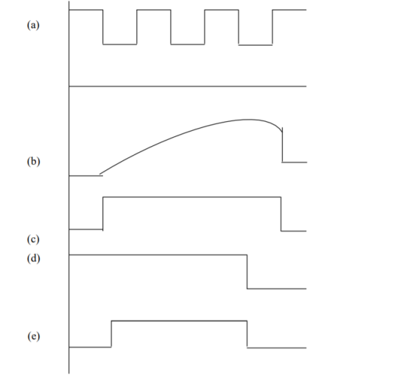
Since C is unclamped, voltage across it rises exponentially through R towards Vcc with a time constant RC (fig b) as shown in below.
After the time period, the upper comparator resets the FF, i.e. Q = 1, Q1 = ON; the output is low that is it discharges the capacitor C to ground potential (fig c)].
The voltage across the capacitor as in fig (b) is given by
Vc = Vcc (1-e -t/RC) ……………. (1)
Therefore, At t = T, Vc = 2/3 Vcc
2/3 Vcc = Vcc(1-e -T/RC)
Or T = RC ln (1/3)
Or T = 1.1RC seconds ……………. (2)
If the reset is applied Q2 = OFF, Q1 = ON, timing capacitor C immediately discharged. The output now will be as in figure (d & e). If the reset is released output will remain low until a negative going trigger pulse is again applied at pin
2. Applications:
Frequency Divider:
The 555 timer as a monostable mode. It can be used as a frequency divider by adjusting the length of the timing cycle tp with respect to the time period T of the trigger input.
To use the monostable multivibrator as a divide by 2 circuit, the timing interval tp must be a larger than the time period of the trigger input.
[Divide by 2 tp-> T of the trigger] By the same concept, to use the monostable multivibrator as a divide by 3 circuit, tp must be slightly larger than twice the period of the input trigger signal & so on, [ divide by 3 tp-> 2T of trigger].
Pulse Width Modulation
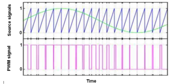
In Pulse Width Modulation the Output Waveform Pulse width of a carrier wave changes in accordance with the value of the incoming (modulating signal) is known as PWM.
It is basically monostable multivibrator. A modulating signal is fed into the control voltage (pin 5). Internally, the control voltage is adjusted to 2/3 Vcc externally applied modulating signal changes the control voltage level of upper comparator.
As a result, the required to change the capacitor up to threshold voltage level changes, giving PWM output.
The 555 timers as an Astable Multivibrator:
An Astable multivibrator, often called a free running multivibrator, is a rectangular wave generating circuit. Unlike the monostable multivibrator, this circuit does not require an external trigger to change the state of the output, hence the name free running. However, the time during which the output is either high or low is determined by 2 resistors and capacitors, which are externally connected to the 55 timers.
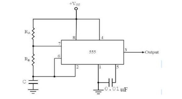
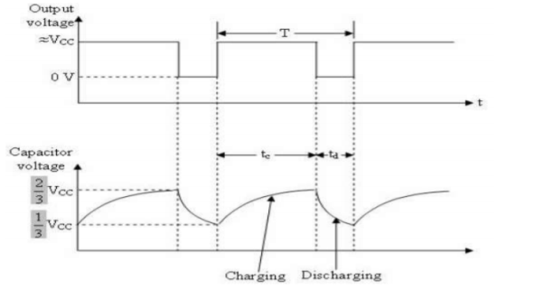
The above figures show the 555 timer connected as an astable multivibrator and its model graph.
Initially, when the output is high ,Capacitor C starts charging toward Vcc through RA & RB. However, as soon as voltage across the capacitor equals 2/3 Vcc. Upper comparator triggers the FF & output switches low.
When the output becomes Low: Capacitor C starts discharging through RB and transistor Q1, when the voltage across C equals 1/3 Vcc, lower comparator output triggers the FF & the output goes High. This cycle repeats. The capacitor is periodically charged & discharged between 2/3 Vcc& 1/3 Vcc respectively.
The time during which the capacitor charges from 1/3 Vcc to 2/3 Vcc equal to the time the output is high & is given by
Tc = (RA+RB)C ln 2……………(1)
Where [ln 2 = 0.69] = 0.69 (RA+RB)C Where RA & RB are in ohms. And C is in farads.
Similarly, the time during which the capacitors discharges from 2/3 Vcc to 1/3 Vcc is equal to the time, the output is low and is given by, tc = RB C ln 2 td = 0.69 RB C …………………..(2)
Where RB is in ohms and C is in farads.
Thus the total period of the output waveform is T = tc + td = 0.69 (RA+2RB)C …………….(3)
This, in turn, gives the frequency of oscillation as,f 0 = 1/T = 1.45/(RA+2RB)C ………(4)
Equation 4 indicates that the frequency f 0 is independent of the supply voltage Vcc. Often the term duty cycle is used in conjunction with the astable multivibrator.
The duty cycle is the ratio of the time tc during which the output is high to the total time period T.
It is generally expressed as a percentage. % duty cycle = (tc / T )* 100 %
DC = [(RA+RB)/ /(RA+2RB)] * 100
Applications:
Square wave oscillator:
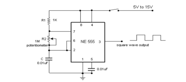
Without reducing RA = 0 ohm, the astable multivibrator can be used to produce square wave output. Simply by connecting diode D across Resistor RB. The capacitor C charges through RA & diode D to approximately 2/3 Vcc& discharges through RB & Q1 until the capacitor voltage equals approximately 1/3 Vcc, then the cycle repeats.
To obtain a square wave output, RA must be a combination of a fixed resistor & potentiometer so that the potentiometer can be adjusted for the exact square wave.
Free – running Ramp generator:
The astable multivibrator can be used as a free – running ramp generator when resistor RA & RB are replaced by a current mirror.
The current mirror starts charging capacitor C toward Vcc at a constant rate.
When voltage across C equals to 2/3 Vcc, upper comparator turns transistor Q1 ON & C rapidly discharges through transistor Q1.
When voltage across C equals to 1/3 Vcc, lower comparator switches transistor OFF & then capacitor C starts charging up again.
Thus, the charge – discharge cycle keeps repeating.
The discharging time of the capacitor is relatively negligible compared to its charging time.
The time period of the ramp waveform is equal to the charging time & is approximately is given by, T = VccC/3IC ………………………… (1)
IC = (Vcc - VBE)/R = constant current
Therefore the free – running frequency of ramp generator is f 0 = 3IC/ Vcc C ……………………….(2)
The third section of the PLL is the voltage-controlled oscillator. The VCO generates an output frequency that is directly proportional to its input voltage.
Typical example of VCO is Signetics NE/SE 566 VCO, which provides simultaneous square wave and triangular wave outputs as a function of input voltage.
The block diagram of the VCO is shown in Figure.

The frequency of oscillations is determined by three external R1 and capacitor C1 and the voltage VC applied to the control terminal 5.
The triangular wave is generated by alternatively charging the external capacitor C1 by one current source and then linearly discharging it by another.
The charging and discharging levels are determined by Schmitt trigger action. The Schmitt trigger also provides square wave output. Both the wave forms are buffered so that the output impedance of each is 50 ohms.
In this arrangement the R1C1 combination determines the free running frequency and the control voltage VC at pin 5 is set by voltage divider formed with R2 and R3.
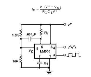
The initial voltage VC at pin 5 must be in the range Where +V is the total supply voltage.The modulating signal is ac coupled with the capacitor C and must be < R1< 20KΩ. For afixed VC and constant C1, the frequency fo can be varied over a 10:1 frequency range by the choice of R1 between 2KΩ< R1< 20KΩ.
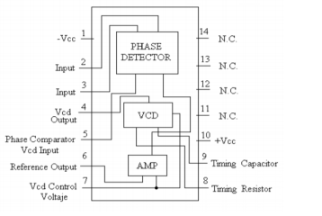
(a)Pin Configuration of IC 565
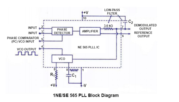
Fig (a) and (b) shows the pin diagram and block diagram of IC 565 PLL. PLL consists of phase detector, amplifier, low pass filter and VCO.
As shown in the block diagram the phase locked feedback loop is not internally connected. Therefore, it is necessary to connect output of VCO to the phase comparator input, externally.
In frequency multiplication applications a digital frequency divider is inserted into the loop that is between pin 4 and pin 5.
The centre frequency of the PLL is determined by the free-running frequency of the VCO and it is given by
f o = 1.2 / 4 R1 C1
R1 and C1 – external resistor and capacitors connected to pin 8 and 9.
The values of R1 and C1 are adjusted in such a way that the free running frequency will be at the centre of the input frequency range.
The values of R1 are restricted from 2 kΩ to 20 kΩ,but a capacitor can have any value. A capacitor C2 connected between pin 7 and the positive supply forms a first order low pass filter with an internal resistance of 3.6 kΩ.
The value of filter capacitor C2 should be large enough to eliminate possible demodulated output voltage at pin 7 to stabilize the VCO frequency.
The PLL can lock to and track an input signal over typically ±60% bandwidth w.r.t fo as the centre frequency. The lock range fL and the capture range fc of the PLL are given by the following equations.
FL = ± 8 fo/V
Where fo = free running frequency
V = (+V) – (-V) volts
And
Fc = ± fL / 2π (3.6) 10 3 C2
From the above equation the lock range increases in input voltage but decreases with increase in supply voltage.
The two inputs to phase detector allows direct coupling of an input signal provided that there is there is no dc voltage difference between the pins and dc resistances seen from pins 2 and 3 are equal.
Analog multiplier is an electronic circuit where the output voltage at any instant is proportional to the product of instantaneous value of two individual input voltages.
Some of the important applications of these multipliers are multiplication, division, squaring and square – rooting of signals, modulation, and demodulation.
These analog multipliers are available as integrated circuits consisting of op-amps and other circuit elements.
The Schematic of a typical analog multiplier, namely, AD633 is shown in figure.
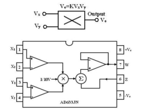
Multiplier IC and its symbol
The AD633 multiplier is a four – quadrant analog multiplier.
It possesses high input impedanceand this characteristic makes the loading effect on the signal source negligible.
It can operate with supply voltages ranging from ±18V.
IC does not require external components.
The typical range of the two input signals is ±10V.
Schematic representation of a multiplier:
The schematic representation of an analog multiplier is shown in figure above.
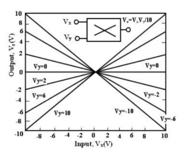
The output V0 is the product of the two inputs Vx and Vy is divided by a reference voltage Vref.
Normally, the reference voltage Vref is internally set to 10V. Therefore,
V0 =VxVy/10.
In other words, the basic input – output relationship can be defined by KVx Vy when K = 1/10, a constant.
Thus, for peak input voltages of 10V, the peak magnitude of output voltage is 1/10 *10 *10 =10V.
Thus, it can be noted that, as long as Vx < 10V and Vy < 10V, the multiplier output will not saturate.
Multiplier quadrants:
The transfer characteristics of a typical four-quadrant multiplier are shown in figure. Both the inputs can be positive or negative to obtain the corresponding output as shown in the transfer characteristics.
Applications of Multiplier ICs:
The multiplier ICs are used for the following purposes:
1. Voltage Squarer
2. Frequency doublers
3. Voltage divider
4. Square rooter
5. Phase angle detector
6. Rectifier
References:
Basic Electronics (VTU) by Professor D Chattopadhyay , Professor P C Rakshit, New Age International (P) Ltd., Publishers
Basic Electronics ByTheraja B.L.
CIRCUIT FUNDAMENTALS and BASIC ELECTRONICS Ashish Chaudhury and R. K. Verma.
Basic Electronics by D P Kothari, I J Nagrath