Unit 5
Application ICs
LM 78XX

LM 78XX series is a three terminal positive regulator available in TO-220 package.
Here each type uses internal current limiting, thermal shut down and safe area protection for making it indestructible.
If enough heat sinking is given, they deliver more than 1A output current.
They can be used with external components to obtain adjustable voltages and currents.
The available voltages are: 5,6,8,9,10,12,15,18 and 24V.
LM 79XX
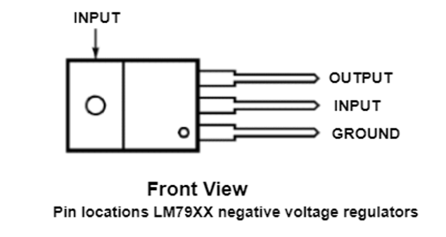
LM79XX series of 3-terminal regulators is available with fixed output voltages of -5V, -12V, and -15V.
These devices require compensation capacitor 1uF solid tantalum or 25uF aluminium electrolytic at the output.
It is a series packaged in the TO-220 power package which is capable of supplying 1.5A of output current with proper heat sinking.
As in LM78XX series they use internal current limiting safe area protection and thermal shutdown for protection against virtually all overload conditions.
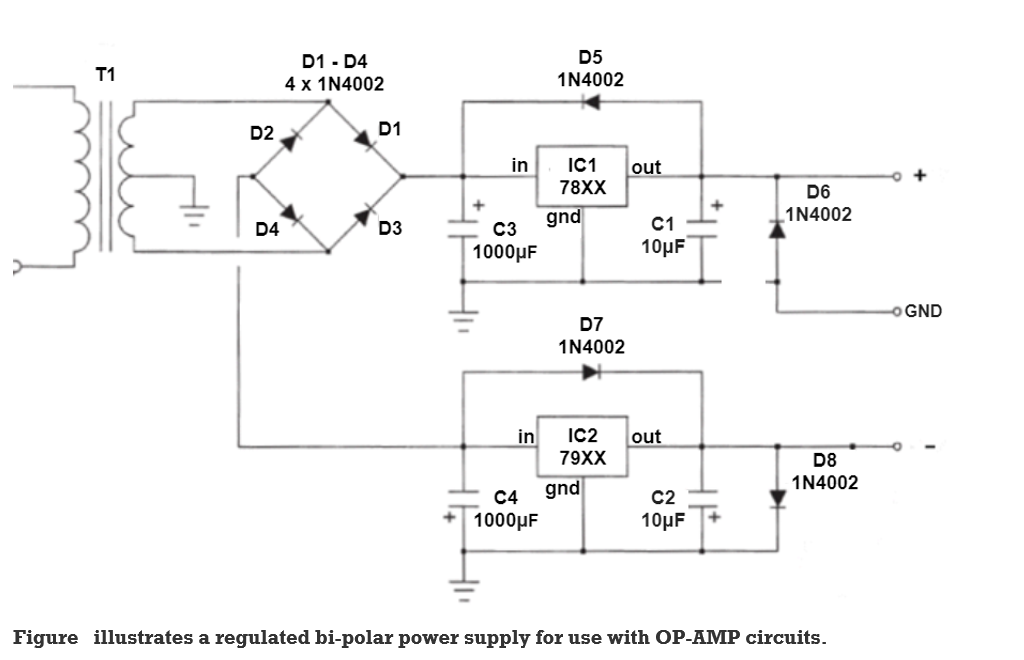
Figure shows the electrical connections on the LM79XX series
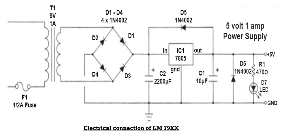
The figure shows 5 volt general purpose power supply .
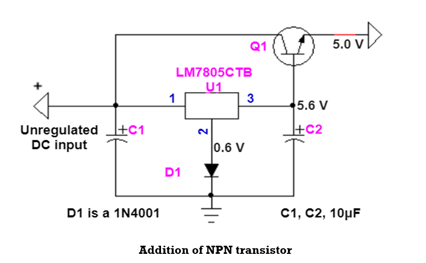
In the figure a NPN pass transistor is added such that 2N3055 is used to boost output current to several amps.
Diode D1 is added to compensate for the voltage drop across the base-emitter junction of Q1.
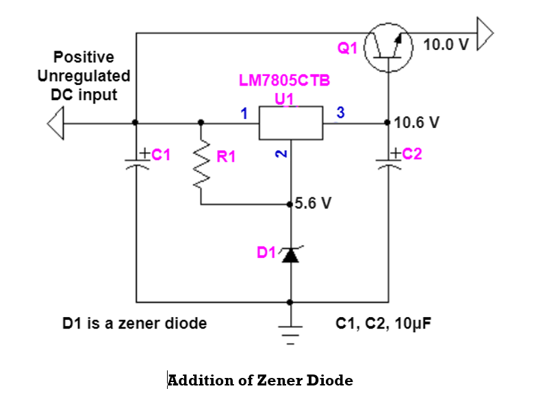
In the figure below 5.6 voltzener diode is added for D1. By using zener any number of odd voltage requirements can be produced.
Q1 works the same as in figure or could be left out and a 5 volt Zener is used if current requirement is under 1 amp.
LM317 Voltage Regulator
Features:
LM 317 is a 3 terminal adjustable voltage regulator that can supply an output voltage which can be adjusted from 1.2 V to 37 V.
It supplies more than 1.5 of load current to load.
LM 317 has 3 pins as shown in the figure below:
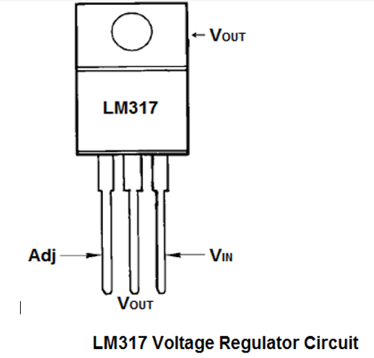
The first pin is the Adjustable pin which allows for adjustable voltage output. To adjust output the R2 resistance is swapped for a different resistance value. This creates adjustable voltages.
The middle is Vout– This pin outputs the regulated voltage. For example, it receives 12V as input and produce 10V as constant output voltage.
The right pin is VIN– It receives the incoming voltage which must be regulated to a specified voltage.
In order to obtain the required output voltage the value of the resistor has to be changed in the Adj pin of the voltage regulator.
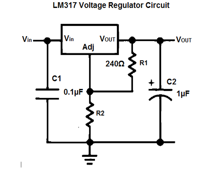
In the above diagram two resistors of the voltage regulators are connected. These resistors determine the voltage that the voltage regulator adjusts to the outputs.
The voltage that the adjustable regulator outputs is given by
Vout = 1.25 V ( 1 + R2 / R1)
Form the above equation the greater R2 increases greater the output voltage.
For example, suppose we put 12 volts into the voltage regulator and regulate it down to 5V then based on the formula to obtain 5V in LM 317 the value of R2 should be 720 Ω.
Using the above circuit use multimeter to check the output voltage across 1μF or across the resistors. The voltage will be approximately 5V. Now if we swap out the R2 resistor and place 1.5 K resistor in place then the output voltage will be approximately 10V.
This is the advantage of voltage regulators. You can adjust to any voltage within the range the voltage regulator supports.
LM 317 Working
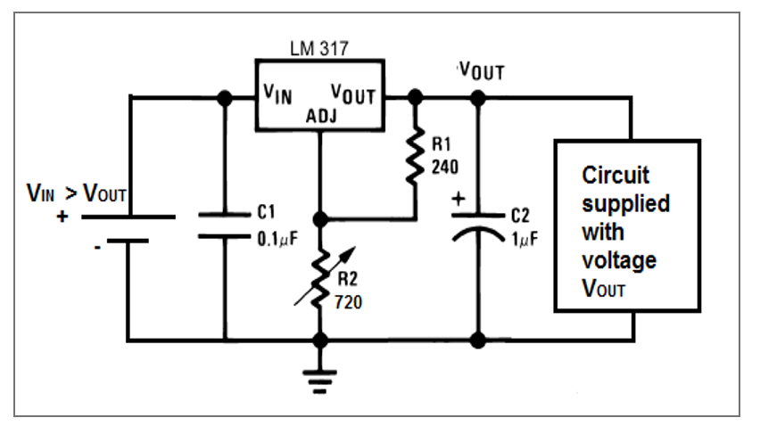
In this circuit when we add DC voltage supply to VIN pin of the regulator, Vin receives the incoming voltage which the chip will regulate down. The voltage which enters this pin must be greater than the incoming voltage. In order to get Vout voltage Vin >Vout .In this circuit, we want a regulated 5VDC as output.
Therefore, VIN must be greater than 5 volts.
Consider the adjustable pin (Adj). This is the pin which allows us to adjust the voltage to the level we want. Since we want 5 volts to be output, we must calculate which value of R2 will yield an output of 5 volts.
Using the formula for the output voltage,
VOUT= 1.25V (1 + R2/R1).
Consider R1=240Ω,
Therefore 5V= 1.25V (1 + R2/240Ω),
Hence, R2=720Ω.
So, with R2 being a value of 720Ω, the LM317 will output 5V if fed an input voltage greater than 5 volts.
LM 723
LM 723 is a changeable voltage regulator used in the series regulator application with 150 mA current output without the exterior pass transistor.
If we use external transistor then it supplies 10A current to drive the load. The maximum voltage for input is 40V and the o/p is 3V – 40 V
LM723 Pin Configuration
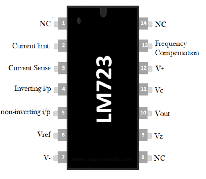
LM723 Pin Diagram
- Pin1 (NC): Not connected
- Pin2 (Current Limit): This pin is used to limit the current
- Pin3 (Current Sense): This pin is used in foldback application as well as to limit the current
- Pin4 (Inverting Input): This pin provides stable o/p voltage
- Pin5 (Non-inverting Input): This pin is used to supply a reference voltage to the inside of the operational amplifier.
- Pin6 (Vref): This pin provides an almost 7v reference voltage
- Pin7 (-Vcc): GND (Ground) Pin
- Pin8 (NC): Not connected
- Pin9 (Vz): This pin is generally used to make negative regulators
- Pin10 (Vout): This is the o/p pin
- Pin11 (Vc): This is the series pass transistor’s collector input. Generally, it is connected directly to the +ve voltage supply if an exterior transistor is not used.
- Pin 12 (V+): This is the input of the positive supply
- Pin13 (Frequency Compensation): This pin assists in decreasing noise with a 100pf capacitor
- Pin 14 (NC): Not connected.
Features:
The maximum input supply voltage will be 40V.
Offers modifiable o/p from 3volts to 37volts.
ICs used for making switching & linear regulator.
Supplies 10A o/p current with the help of an external pass transistor.
These ICs are used for different operations such as positive, negative, series, floating, and shunt.
Specifications
- The maximum i/p voltage is 40v
- The reference voltage is always 7 volts
- Ripple rejection is 74 dB
- The current supply from Vz pin is 25mA
- The output voltage ranges from 3volts to 37 volts
- The range of operating temperature will be from -55°C to +150°C
- The current supply from Vref pin is 15mA
- The line and load regulation of 0.01%Vout & 0.03% Vout
LM723 Internal Block Diagram
The figure shows the internal block diagram of the LM723 IC. There are two blocks namely the error amplifier and the reference voltage generator.
In the reference block , Zener diode is forced to work at set point so the output of Zen which is more has stable current supply which produces stable voltage (7.15V) along with the amplifier on Vref pin of IC.
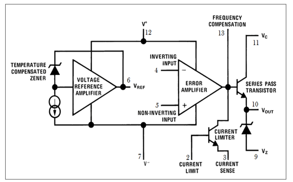 LM723 Internal Block Diagram
In the error amplifier block, it consists of series pass Q1 transistor, an error amplifier, & a transistor which limits the current.
This amplifier is used to contrast the o/p voltage which is given at inverting i/p terminal throughout feedback toward the Vref-reference voltage given at the non-inverting terminal.
The two connections are not offered internally and have to be externally offered in accordance with required output voltage. The conduction of the transistor Q1 is controlled by the error signal. It is this transistor that controls the output voltage.
Advantages of LM723 Voltage Regulator
The advantages of LM723 voltage regulator include proven, low noise, the voltage range is wide, support for external pass transistors, recompense by the user, extremely flexible, complete temperature range accessible, and economical
LM 317 is a 3 terminal positive voltage regulator with 1.25 to 37 volts output voltage range.
LM117 / LM217 / LM317 are variable voltage regulator characteristics
To obtain this voltage variation 2 external resistor are required in which one of them is variable resistor. The two main characteristics of voltage regulator are current limitation and thermal protection against overloads
The voltage between ADJ and OUT terminals is always 1.25 volts and therefore current flowing through the resistor R1 is:
I R1 = V / R1 = 1.25 / R1 ---------------------------(1)
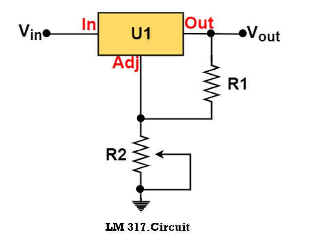
The current through resistor R1 is IR1 which is the same current that circulates through resistor R2.
Then the voltage on resistor R2 is: VR2 = IR1 x R2---------------------- (2)
If IR1 (1) is substituted into the formula (2), the following equation is obtained: VR2 = 1.25 x R2/R1.
Since the output voltage is:
Vout = VR1 + VR2, then …
Vout = 1.25 V + (1.25 x R2/R1) V.
Vout = 1.25 V (1 + R2/R1) V.
R2 is the variable resistor . Let R1 = 240 ohms Then by substituting we get R2 = 5K or 3K (potentiometer)
The IADJ current was neglected, since it has a maximum value of 100uA and it remains constant with load and input voltage variations.
To improve the regulation, resistor R1 must be placed as close as possible to the regulator, while the R2 resistor ground terminal must be connected as close as possible to the ground connection of the load.
Circuit operation
To optimize the LM317 variable voltage regulator circuit operation, some additional elements are incorporated into the design.
See the diagram below.
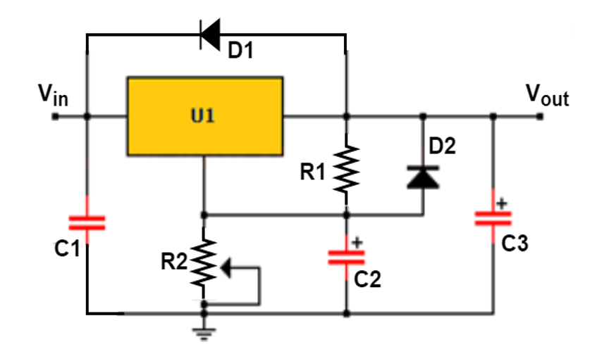
A 0.1uF capacitor (C1) is placed at the input terminal if the voltage regulator is away from the rectification components.
A 1uF tantalum capacitor or a 25uF electrolytic capacitor (C3) is placed at the output terminal (OUT) to improve the transient’s response.
A 10uF electrolytic capacitor (C2) is placed in parallel with resistor R2, to improve rejection of the ripple voltage.
A 1N4001 diode (D1) is placed to protect the regulator against possible short circuits at the regulator input.
A 1N4001 diode (D2) is placed to protect the regulator against possible short circuits in its output when capacitors are discharged.

A basic switching regulator consists of 4 major components,
1. Voltage source Vin
2. Switch S1
3. Pulse generator Vpulse
4. Filter F1 1.
Voltage Source Vin:
- It may be any dc supply – a battery or an unregulated or a regulated voltage.
- The voltage source must satisfy the following requirements:
- It must supply the required output power & the losses associated with the switching regulator.
- It must be large enough to supply sufficient dynamic range for line & load regulations.
- It must be sufficiently high to meet the minimum requirement of the regulator system to be designed.
- It may be required to store energy for a specified amount of time during power failures.
Switch S1:
It is typically a transistor or thyristor connected as a power switch & is operated in the saturated mode.
The pulse generator output alternately turns the switch ON & OFF
Pulse generator Vpulse:
- It provides an asymmetrical square wave varying in either frequency or pulse width called frequency modulation or pulse width modulation, respectively.
- The most effective frequency range for the pulse generator for optimum efficiency is 20 KHz.
- This frequency is inaudible to the human ear & also well within the switching speeds of most inexpensive transistors & diodes.
- The duty cycle of the pulse wave form determines the relationship between the input & output voltages.
- The duty cycle is the ratio of the on- time ton, to the period T of the pulse waveform.
T =ton toff
Where ton = On-time of the pulse waveform
Toff=off-time of the pulse wave form
T = time- period = ton + toff = 1/frequency or T = 1/f
Typical operating frequencies of switching regulator range from 10 to 50khz.
Lower operating frequency improve efficiency & reduce electrical noise, but require large filter components (inductors & capacitors).
Filter F1:
It converts the pulse waveform from the output of the switch into a dc voltage. Since this switching mechanism allows a conversion like transformers, the switching regulator is often referred to as dc transformer.
The output voltage Vo of the switching regulator is a function of duty cycle & the input voltage Vin.
Vo is expressed as follows, Vo = ton/ Vin x T
This equation indicates thatif time- period T is constant, Vo is directly proportional to the ON-time, ton for a given value of Vin. This method of changing the output voltage by varying ton is referred to as pulse width modulation.
Similarly, if ton is held constant, the output voltage Vo is inversely proportional to the period T or directly proportional to the frequency of the pulse waveform.
This method of varying the output voltage is referred to as frequency modulation (FM).
Features of LM380:
1. Internally fixed gain of 50 (34dB)
2. Output is automatically self- centring to one half of the supply voltage.
3. Output is short circuit proof with internal thermal limiting.
4. Input stage allows the input to be ground referenced or ac coupled.
5. Wide supply voltage range (5 to 22V).
6. High peak current capability.
7. High impedance.
8. Low total harmonic distortion
9. Bandwidth of 100KHz at Pout = 2W & RL = 8Ω
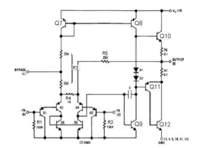
LM380 circuit description:
It is connected of 4 stages:
- PNP emitter follower
- Different amplifier
- Common emitter
- Emitter follower
PNP Emitter follower:
The input stage is emitter follower composed of PNP transistors Q1 & Q2 which drives the PNP Q3-Q4 differential pair.
The choice of PNP input transistors Q1 & Q2 allows the input to be referenced to ground that the input can be direct coupled to either the inverting & non-inverting terminals of the amplifier.
Differential Amplifier:
The current in the PNP differential pair Q3-Q4 is established by Q7, R3 & +V.
The current mirror formed by transistor Q7, Q8 & associated resistors then establishes the collector current of Q9.
Transistor Q5 & Q6 constitute of collector loads for the PNP differential pair.
The output of the differential amplifier is taken at the junction of Q4 & Q6 transistors & is applied as an input to the common emitter voltage gain.
Common Emitter:
Common Emitter amplifier stage is formed by transistor Q9 with D1, D2 & Q8 as a current source load.
The capacitor C between the base & collector of Q9 provides internal compensation & helps to establish the upper cut-off frequency of 100 KHz.
Since Q7 & Q8 form a current mirror, the current through D1 & D2 is approximately the same as the current through R3.
D1 & D2 are temperature compensating diodes for transistors Q10 & Q11 in that D1 & D2 have the same characteristics as the base-emitter junctions of Q11. Therefore, the current through Q10 & (Q11-Q12) is approximately equal to the current through diodes D1 & D2.
(Output stage) - Emitter follower:
Emitter follower formed by NPN transistor Q10 & Q11.
The combination of PNP transistor Q11 & NPN transistor Q12 has the power capability of an NPN transistors but the characteristics of a PNP transistor.
The negative dc feedback applied through R5 balances the differential amplifier so that the dc output voltage is stabilized at +V/2;
To decouple the input stage from the supply voltage +V, by- pass capacitor in order of micro farad should be connected between the by- pass terminal (pin 1) & ground (pin 7).
The overall internal gain of the amplifier is fixed at 50. However, gain can be increased by using positive feedback.
The ICL8038 is a function generator chip, capable of generating triangular, square, sine, pulse and sawtooth waveforms.
The sine, square and triangular waveforms can be made simultaneously. To control parameters like frequency, duty cycle and distortion there is an option provided.
- This is the best function generator. It must be operated from a dual power supply.
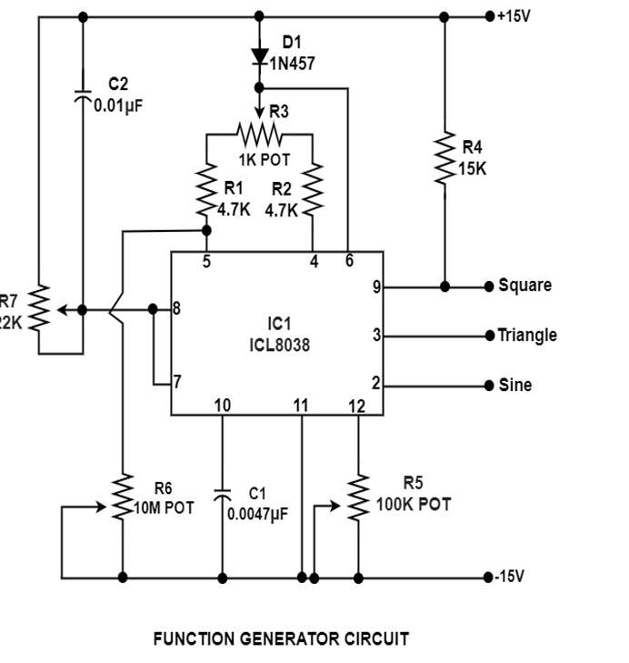
- The circuit needs a dual power supply +15 -15V power supply as shown in the circuit
- The frequency of the output wave form can be adjusted through R7 which is 100K POT.
- The duty cycle can be adjusted using R3, a 1K POT.
- The distortion of the wave form can be adjusted using R5, a 100K POT.
- Square,triangle & sine waveforms can be obtained simultaneously at pins 9,3,2 respectively.
References:
Basic Electronics (VTU) by Professor D Chattopadhyay , Professor P C Rakshit, New Age International (P) Ltd., Publishers
Basic Electronics ByTheraja B.L.
CIRCUIT FUNDAMENTALS and BASIC ELECTRONICS Ashish Chaudhury and R. K. Verma.
Basic Electronics by D P Kothari, I J Nagrath