Module 2
8051 Architecture
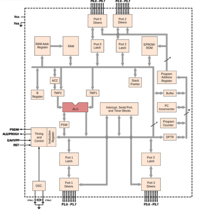
8051 microcontrollers were designed by Intel in 1981. It is an 8-bit microcontroller. It is built with 40 pins DIP (dual inline package), 4kb of ROM storage and 128 bytes of RAM storage, 2 16-bit timers. It consists of four parallel 8-bit ports, which are programmable as well as addressable as per the requirement.
The reasons for the popularity of 8051 Microcontroller are –
● Simple to integrate in any electronic device.
● Affordable.
● Simple architecture.
● Easy instruction set.
● Low computing power.
The CPU acts as a mind of any processing machine. It synchronizes and manages all processes that are carried out in microcontrollers. The user has no power to control the functioning of the CPU. It interprets the program stored in ROM and carries out from storage and then performs it projected duty. CPUs manage the different types of registers available in 8051 microcontrollers.
It is the heart of the Microcontroller that mainly comprises an Arithmetic Logic Unit (ALU) and a Control Unit (CU) and other important components. The CPU is the primary device in communicating with peripheral devices like Memory, Input and Output.
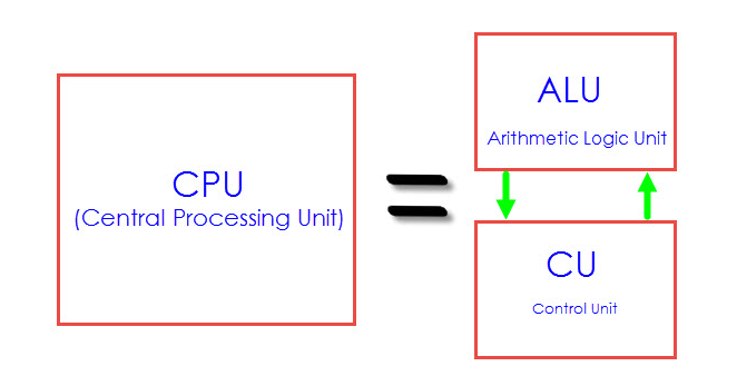
ALU performs all arithmetic and logical functions.
Addition, subtraction with carry, and multiplication are categorized as arithmetic operations.
Logical AND, OR and exclusive OR (XOR) as logical operations.
A bus consists of a group of wires to transfer data from one location to another within the system. Buses reduce the number of paths or cables needed to set up connection between components.
There are two kinds of buses - Data Bus and Address Bus
Data Bus: The purpose of a data bus is to transfer data. It acts as a channel for data to travel.
Address Bus: The purpose of address bus is to transfer information but not data. The information tells from where within the components, the data should be sent to or received from.
Control bus - carries control signals from the processor to other components. The control bus also carries the clock's pulses. The control bus is unidirectional
Registers are known as data storage devices. There are two registers namely Register A and Register B. Register A is used as an accumulator and Register B as general -purpose register. The output of mathematical and logical instructions are stored in these registers.
The operations of addition, subtraction, multiplication and division are performed by Register A. Register B is for multiplication and division which are carried by Register A. For data transfers between microcontroller and external memory Register A is involved.
8051 has four Register banks.
When the 8051 is first booted up Register bank 0 (addresses 00h through 07h) is used by default.
The internal memory supports 4 register banks.
The first 8 bytes (00h – 07h) are “register bank 0”.
Followed by Bank1 (08 – 0F),
Bank2 (10 – 17),
Bank3 (18 – 1F).
Register banks reside in the first 32 bytes of Internal RAM.
PSW (PROGRAM STATUS WORD)
This is an 8-BIT register. The Program Status Word (PSW) contains status bits that reflect the current CPU state.
A (ACCUMULATOR)
Accumulator is an 8-bit register.It holds the result of most arithmetic and logic operations. This register is usually accessed by direct addressing. It is both byte and bit addressable.
B (EXTENSION REGISTER)
The major purpose of the B(Extension register) register is executing multiplication and division. This register is directly accessed when we are writing our code in assembly language. The 8051 microcontroller has a single instruction for multiplication (MUL) and division (DIV).
SP (STACK POINTER)
Stack pointer is an 8- bit register, the direct address of SP is 81H and it is only byte addressable that means individual bits of stack pointer cannot be accessed. The content of the stack pointer points to the last stored location of the system stack. T
To store something new in the system stack, the SP must be incremented by 1 first and then execute the “store” command.
Push increments the SP and writes data.
● POP reads data and then decrements the SP.
● Stack is kept in the internal RAM and is restricted to 128 bytes.
● Top most address of the stack is 7F.
DPTR (DATA POINTER REGISTER)
This is a 16 bit register. It is used to access external code or data memory
The Data Pointer (DPTR) is the 8051’s only user-accessible 16-bit (2-byte) register.
8051 microcontrollers also have 7 Special Function Registers (SFRs). They are:
1. Serial Port Data Buffer (SBUF)
2. Timer/Counter Control (TCON)
3. Timer/Counter Mode Control (TMOD)
4. Serial Port Control (SCON)
5. Power Control (PCON)
6. Interrupt Priority (IP)
7. Interrupt Enable Control (IE)
- SBUF(Serial Buffer Register)

This is a serial buffer register which is used to transmit or receive data through it.
For holding data SBUF (Serial Port Data Buffer) register;
Manage data communication SCON (Serial Control) register
Managing data transfer rate PCON (Power Control) register
RXD and TXD establish serial networks.
SBUF register has 2 parts
For storing the data to be transmitted use TXD pin
For receiving data from other sources use an RXD pin.
Serial data communication operates in four modes. They are serial data
1. Mode 0 (shift register mode)
2. Mode 1 (standard UART)
3. Mode 2 (multiprocessor mode)
4. Mode 3
2. TCON Register
TCON is another register used to control operations of counters and timers in microcontrollers. It is an 8-bit register wherein four upper bits are responsible for timers and counters and lower bits are responsible for interrupts.

Bit | Symbol | TCON Bit Function |
7 | TF1l | Timer 1 Overflow flag. Set when the timer rolls from all 1's to 0. Cleared when processor vectors to execute interrupt service routine located at program address 001Bh. |
6 | TR1l | Timer 1 run control bit. Set to 1 by program to enable timer to count; cleared to 0 by program to halt timer. |
5 | TF0 l | Timer 0 Overflow flag. Set when the timer rolls from all 1's to 0. Cleared when processor vectors to execute interrupt service routine located at program address 000Bh. |
4 | TR0l | Timer 0 run control bit. Set to 1 by program to enable timer to count; cleared to 0 by program to halt timer. |
3 | IE1 l | External interrupt 1 Edge flag. Set to 1 when a high-to-low edge signal is received on port 3.3 . Cleared when processor vectors to interrupt service routine at program address 0013h. Not related to timer operations. |
2 | IT1 l | External interrupt 1 signal type control bit. Set to 1 by program to enable external interrupt 1 to be triggered by a falling edge signal. Set to 0 by program to enable a low-level signal on external interrupt 1 to generate an interrupt. |
1 | IE0 l | External interrupt 0 Edge flag. Set to 1 when a high-to-low edge signal is received on port 3.2 (INT0). Cleared when processor vectors to interrupt service routine at program address 0003h. Not related to timer operations. |
0 | IT0 l | External interrupt 0 signal type control bit. Set to 1 by program to enable external interrupt 1 to be triggered by a falling edge signal. Set to 0 by program to enable a low-level signal on external interrupt 0 to generate an interrupt. |
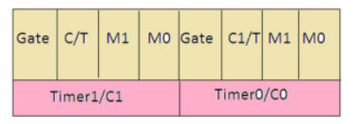
3.Timer/Counter Mode Control (TMOD)
| |
7 | Gate -- OR gate enable bit which controls RUN/STOP of timer 1. Set to 1 by program to enable the timer to run if bit TR1 in TCON is set and signal on external interrupt INT1 is high. Cleared to 0 by program to enable time to run if bit TR1 is set. |
6 | C/T -- Set to 1 by program to make timer 1 act as a counter by counting pulses from external input pins 3.5. Cleared to zero by program to make the timer act as a timer by counting internal frequency. |
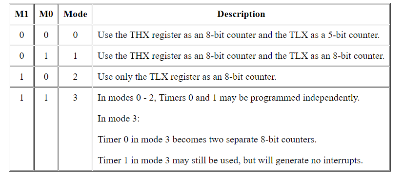
5 | M1 -- Timer/counter operating mode select bit 1. Set/cleared by program to select mode. |
4 | M0 -- Timer/counter operating mode select bit 0. Set/cleared by program to select mode. |
3 | Gate -- OR gate enable bit which controls RUN/STOP of timer 0. Set to 1 by program to enable the timer to run if bit TR0 in TCON is set and signal on external interrupt INT0 is high. Cleared to 0 by program to enable time to run if bit TR0 is set. |
2 | C/T -- Set to 1 by program to make timer 0 act as a counter by counting pulses from external input pin 3.4. Cleared to zero by program to make the timer act as a timer by counting internal frequency. |
1 | M1 -- Timer/counter operating mode select bit 1. Set/cleared by program to select mode. |
0 | M0 -- Timer/counter operating mode select bit 0. Set/cleared by program to select mode. |
4. Serial Port Control (SCON)
● Serial port control and status register is the special function register SCON.
● This register not only contains the mode selection bits but also the 9th data bit for transmit and receive (TB8 and RB8) and the serial part interrupt bits (TI and RI)

SM0 | SM1 | Mode | Description | Baud Rate |
0 | 0 | 0 | 8-Bit Synchronous Shift Register Mode | Fixed Baud Rate ( Frequency of oscillator / 12) |
0 | 1 | 1 | 8-bit Standard UART Mode | Variable Baud Rate (Can be set by Timer 1) |
1 | 0 | 2 | 9-bit Multiprocessor Comm. Mode | Fixed Baud Rate ( Frequency of oscillator / 32 or Frequency of oscillator / 64 |
1 | 1 | 3 | 9-bit Multiprocessor Comm. Mode | Variable Baud Rate (Can be set by Timer 1) |
5. Power Control (PCON)
PCON Register: Power control register
PCON (Power Control) register is used to force the 8051 microcontrollers into power-saving mode. The power control register of 8051 contains two power-saving mode bits and one serial baud rate control bit.

Bit 7 – SMOD
1 = Baud rate is doubled in UART mode 1, 2 and 3.
0 = No effect on Baud rate.
Bit 3:2 – GF1 & GF0:
These are general purpose bits for users.
Bit 1 – PD: Power Down
1 = Enable Power-Down mode. In this mode, the Oscillator clock turned OFF and both CPU and peripherals stopped. Hardware reset can cancel this mode.
0 = Disable Power-down mode.
Bit 0 – IDL: Idle
1 = Enable Idle mode. CPU clock turned off whereas internal peripheral modules such as a timer, serial port, interrupts worked normally. Interrupt and H/W reset can cancel this mode.
0 = Disable Idle mode.
6. Interrupt Priority (IP)
We can change the priority levels of the interrupts by changing the corresponding bit in the Interrupt Priority (IP) register as shown in the following figure.
● A low priority interrupt can only be interrupted by the high priority interrupt, but not interrupted by another low priority interrupt.
● If two interrupts of different priority levels are received simultaneously, the request of higher priority level is served.
● If the requests of the same priority levels are received simultaneously, then the internal polling sequence determines which request is to be serviced.

- | IP.6 | Reserved for future use. |
- | IP.5 | Reserved for future use. |
PS | IP.4 | It defines the serial port interrupt priority level. |
PT1 | IP.3 | It defines the timer interrupt of 1 priority. |
PX1 | IP.2 | It defines the external interrupt priority level. |
PT0 | IP.1 | It defines the timer0 interrupt priority level. |
PX0 | IP.0 | It defines the external interrupt of 0 priority level. |
7. Interrupt Enable Control (IE)
This register is responsible for enabling and disabling the interrupt. EA register is set to one for enabling interrupts and set to 0 for disabling the interrupts. Its bit sequence and their meanings are shown in the following figure.

EA IE.7 It disables all interrupts. When EA = 0 no interrupt will be acknowledged and EA = 1 enables the interrupt individually.
- IE.6 Reserved for future use.
- IE.5 Reserved for future use.
ES IE.4 Enables/disables serial port interrupt.
ET1 IE.3 Enables/disables timer1 overflow interrupt.
EX1 IE.2 Enables/disables external interrupt1.
ET0 IE.1 Enables/disables timer0 overflow interrupt.
EX0 IE.0 Enables/disables external interrupt0.
RESET is an active High input. When RESET is set to High, 8051 goes back to the power on state. The 8051 is reset by holding RST high for at least two machine cycles and then returning it low.
There are two method of reset circuit:
1.Power On Reset.
● Initially charging of capacitor makes RST High
● When the capacitor charges fully it blocks DC.
2.Manual Reset
● closing the switch momentarily will make RST High.
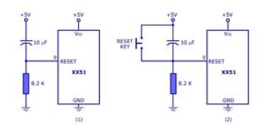
(1) – Power on Reset
(2) Manual Reset
Clock Circuit:
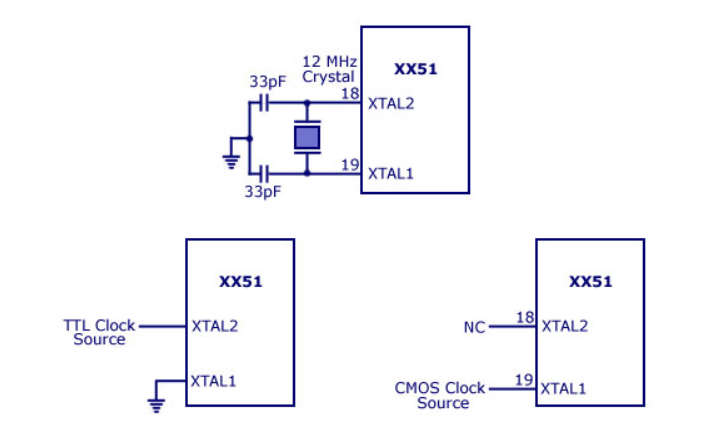
In general cases, a quartz crystal is used to make the clock circuit. The connection is shown in figure (a). In cases of external clock sources the clock frequency limits (maximum and minimum) may change from device to device.
Standard practice is to use 12MHz frequency. If serial communications are involved then its best to use 11.0592 MHz frequency.
The stack is a section of RAM used by the CPU to store information such as data or memory address on a temporary basis. The CPU needs this storage area considering the limited number of registers.
As the stack is a section of a RAM, there are registers inside the CPU to point to it. The register used to access the stack is known as the stack pointer register.
The stack pointer in the 8051 is 8-bits wide, and it can take a value of 00 to FFH. When the 8051 is initialized, the SP register contains the value 07H. This means that the RAM location 08 is the first location used for the stack.
The storing operation of a CPU register in the stack is known as a PUSH, and getting the contents from the stack back into a CPU register is called a POP.
Pushing into the Stack
In the 8051, the stack pointer (SP) points to the last used location of the stack. When data is pushed onto the stack, the stack pointer (SP) is incremented by 1. When PUSH is executed, the contents of the register are saved on the stack and SP is incremented by 1. To push the registers onto the stack, we must use their RAM addresses.
For example, the instruction "PUSH 1" pushes register R1 onto the stack.
Popping from the Stack
Popping the contents of the stack back into a given register is the opposite to the process of pushing. With every pop operation, the top byte of the stack is copied to the register specified by the instruction and the stack pointer is decremented once.
The program counter points to the address of the next instruction to be executed. As the central processing unit [CPU] fetches the opcode from the program ROM, the program counter is incremented to point to the next instruction.
The program counter in the 8051 is 16-bits wide. This means that the 8051 can access program addresses 0000 to FFFFH, a total of 64K bytes of code.
Consider the action of the program counter as fetching and executing a program. First, we examine the list file of the sample program taken from the previous section-IIIa and see how the code is placed in the ROM of an 8051 chip.
1 0000 ORG 0H ;Start at origin 0 2 0000 7D25 MOV R5,#24H ;Load 25H into R5 3 0002 7F34 MOV R7,#34H ;Load 34H into R7 4 0004 7400 MOV A,#0 ;Load 0 into A 5 0006 2D ADD A,R5 ;Add contents of R5 to A,A=A+R5 6 0007 2F ADD A,R7 ;Add contents of R7 to A,A=A+R7 7 0008 2412 ADD A,#12H ;Add to accumulator value 12H 8 000A 80FE HERE:SJMP HERE ;Stay in this loop 9 000C END ;End of asm source file |
8051 microcontrollers have 4 I/O ports each of 8-bits configured as input or output. Hence, total 32 input/output pins allow the microcontroller to be connected with the peripheral devices.
● Pin configuration, that is the pin is configured as 1 for input and 0 for output as per the logic state.
- Input/Output (I/O) pin − All the circuits within the microcontroller must be connected to one of its pins except P0 port because it does not have pull-up resistors built-in.
- Input pin − Logic 1 is applied to a bit of the P register. The output FE transistor is turned off and the other pin remains connected to the power supply voltage over a pull-up resistor of high resistance.
● Port 0 − The P0 (zero) port is characterized by two functions −
- When the external memory is used then the lower address byte (addresses A0A7) is applied on it, else all bits of this port are configured as input/output.
- When P0 port is configured as an output then other ports consisting of pins with built-in pull-up resistor connected by its end to 5V power supply, the pins of this port have this resistor left out.
Input Configuration
If any pin of this port is configured as an input, then it acts as “floats” , that is the input has unlimited input resistance and in-determined potential.
Output Configuration
When the pin is configured as an output, then it acts as an “open drain”. By applying logic 0 to a port bit then appropriate pin will be connected to ground (0V), and applying logic 1, the external output will keep on “floating”.
To apply logic 1 (5V) on this output pin, it is necessary to build an external pullup resistor.
Port 1
P1 is a true I/O port as it does not have any alternative functions as in P0, but this port can be configured as general I/O only. It has a built-in pull-up resistor and is completely compatible with TTL circuits.
Port 2
P2 similar to P0 when the external memory is used. Pins of this port occupy addresses intended for the external memory chip. This port can be used for higher address byte with addresses A8-A15. When no memory is added then this port can be used as a general input/output port similar to Port 1.
Port 3
In this port, functions are similar to other ports except that the logic 1 must be applied to the appropriate bit of the P3 register.
8051 Memory Organization
The 8051 Microcontroller Memory is separated into Program Memory (ROM) and Data Memory (RAM). The Program Memory of the 8051 Microcontroller is used for storing the program to be executed, which means instructions. The Data Memory is used for storing temporary variable data and intermediate results.
Program Memory (ROM) of 8051
The code or instructions which are to be executed are stored in the Program Memory, also called as the ROM of the Microcontroller.
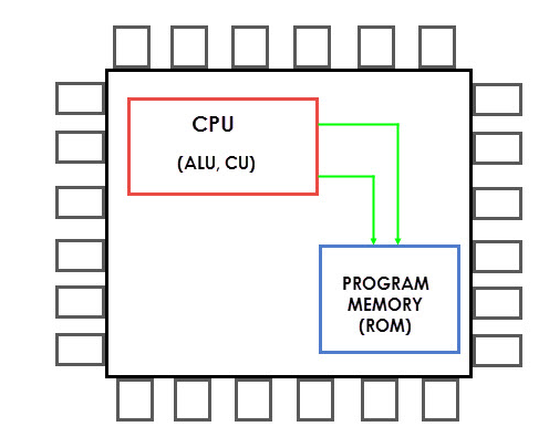
Program Memory
In 4KB Internal ROM, the address space is 0000H to 0FFFH. If the program addresses exceed this value,the CPU will automatically fetch the code from the external Program Memory.
For External Access (EA Pin) must be pulled HIGH at this condition the CPU first fetches instructions from the Internal Program Memory in the address range of 0000H to 0FFFFH .If it exceeds the memory addresses limit, instructions are fetched from external ROM in address range of 1000H to FFFFH.
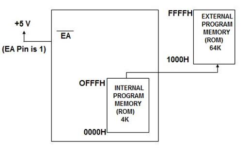
External access
There is also an alternative method to fetch the instructions where the Internal ROM is ignored and instructions are fetched only from External Program Memory(External ROM).
For this purpose, the EA pin must be connected to GND. The memory addresses of external ROM will be from 0000H to FFFFH.
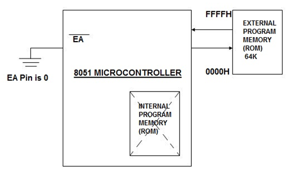
External Program Memory
Data Memory (RAM)
▪ Data Memory or RAM stores temporary data and intermediate results generated during the normal operation of the microcontroller.
▪ Currently, 8051 Microcontroller has 256B of RAM. The first 128B memory addresses from 00H to 7FH are divided into Working Registers. They are organized as Register Banks, Bit – Addressable Area and General Purpose RAM known as Scratchpad area.
▪ The first 128B of RAM (from 00H to 7FH), the first 32B of memory from addresses 00H to 1FH consists of 32 Working Registers organized into four banks with 8 Registers in each Bank.
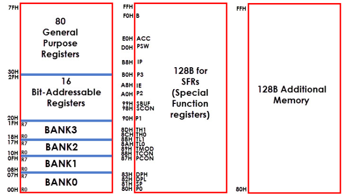
Lower 128B(00H to 07H) Upper 128B(80H-FFH)
(Direct and Indirect Addressing) (Direct Addressing) (Indirect Addressing)
▪ The 4 banks are named as Bank0, Bank1, Bank2 and Bank3. Each Bank consists of 8 registers R0 – R7. Each Register can be addressed either by name or by address.
▪ To address the register by name, first the corresponding bank is selected. In order to select the bank, RS0 and RS1 bits of the Program Status Word (PSW) and Register (RS0 and RS1 are 3rd and 4th bits in the PSW Register) are used.
▪ When addressing these Register for example 12H the corresponding bank may or may not be selected. (12H corresponds to R2 in Bank2).
▪ The next 16B of the RAM that is from 20H to 2FH are Bit – Addressable memory locations. A total of 128 bits can be addressed individually using 00H to 7FH or an entire byte can be addressed as 20H to 2FH.
▪ The final 80B of the internal RAM addresses are from 30H to 7FH which is the general-purpose RAM area that is byte addressable.
▪ These lower 128B of RAM can be addressed directly or indirectly.
The processor decodes the instruction in the instruction register and generates the necessary control signals to execute the instruction. Based on the instruction further operations such as fetching, writing into memory etc takes place.
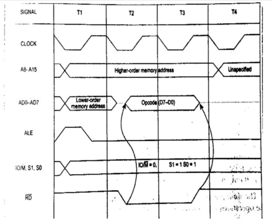
Timing diagram for op-code fetch cycle.
Memory Read Machine Cycle:
The memory read cycle is executed by the processor to read a data byte from memory.
The machine cycle is exactly same to opcode fetch except:
a) It has three T-states
b) The S0 signal is set to 0.
The timing diagram of this cycle is given in
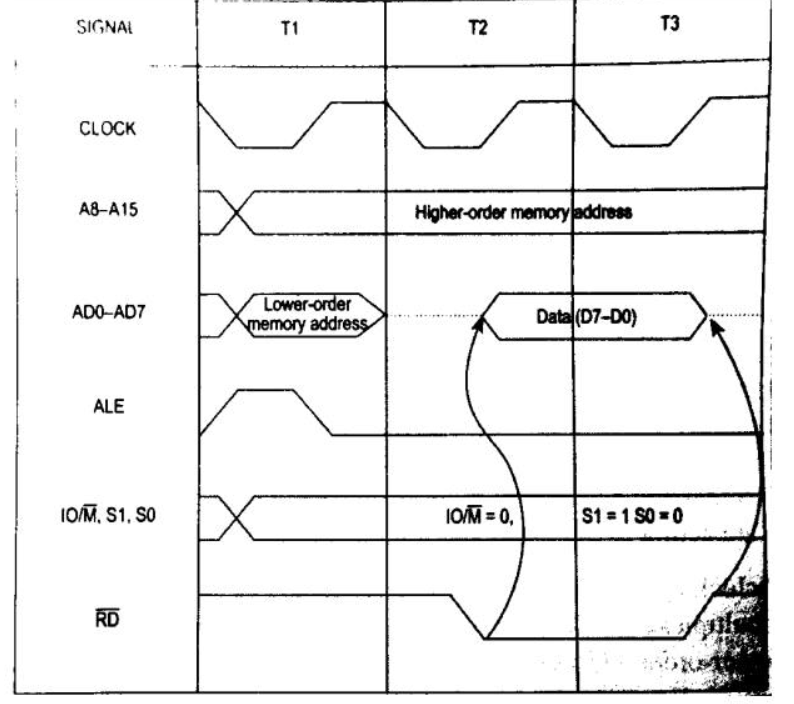
Timing diagram for memory read machine cycle.
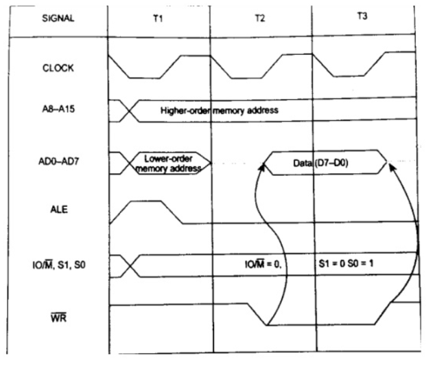
Memory Write Machine Cycle:
The memory write cycle is executed by the processor to write a data byte in a memory location. The processor takes three T-states and ^(WR) signal is made low. The timing diagram of this cycle is given in Figure.

I/O Read Cycle:
The I/O read cycle is executed by the processor to read a data byte from I/O port or from peripheral, which is I/O mapped in the system. The 8-bit port address is placed both in the lower and higher order address bus. The processor takes three T-states to execute this machine cycle. The timing diagram of this cycle is given in Figure
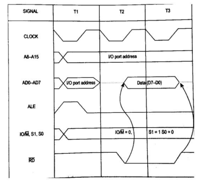
I/O read machine cycle
References:
❖ 8051 Microcontroller: An Applications Based Introduction Book by David Calcutt, Frederick J. Cowan, and Hassan Parchizadeh
❖ 8051 Microcontrollers: Internals, Instructions, Programming, and Interfacing Book by Subrata Ghoshal
❖ C and the 8051: Building efficient applications Book by Thomas W. Schultz
❖ MICROCONTROLLER Book by V. Udayashankara
❖ The 8051/8052 Microcontroller: Architecture, Assembly Language, and Hardware Interfacing Book by Craig Steiner