Module 6
Applications
Light Emitting Diodes are considered as semi- conductor light sources. The commonly used LEDs have a cut-off voltage of 1.7V and current of 10mA. When applied with its required voltage and current it glows with full intensity.
The Light Emitting Diode works similar to a normal PN- diode but it emits energy in the form of light. The color of the light depends on the semiconductors band gap.
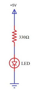
LED
The LED is connected to an AT89C51 microcontroller with the current limiting resistor. The value of this resistor is calculated using the following formula.
R= (V-1.7)/10mA, where V is the input voltage.
The maximum output voltage of microcontrollers is 5V. Hence the calculated value of resistor is 330 Ohms. The resistor can be connected to cathode or the anode of LED.
● Initially, burn the code into the microcontroller.
● Connect the LEDs to the Port0 of the microcontroller.
● Switch on the circuit.
● The LEDs start glowing.
● Switch off the circuit.
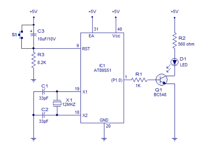
LED Interfacing
▪ In the circuit, push button switch S1, capacitor C3 and resistor R3 forms the reset circuitry.
▪ When S1 is pressed, voltage at the reset pin (pin9) goes high and this resets the chip. C1, C2 and X1 are related to the on -chip oscillator to produces the required clock frequency.
▪ P1.0 (pin1) acts as the output pin. When P1.0 turns high the transistor Q1 is forward biased and the LED gets ON. When P1.0 turns low, the transistor gets cut off and the LED extinguishes.
▪ The transistor driver circuit for the LED can be avoided and the LED can be connected directly to the P1.0 pin along with the series current limiting resistor(~1K).
▪ The time for which P1.0 turns high and low (time period of the LED) is determined by the program.
Program:
START: CPL P1.0
ACALL WAIT
SJMP START
WAIT: MOV R4,#05H
WAIT1: MOV R3,#00H
WAIT2: MOV R2,#00H
WAIT3: DJNZ R2,WAIT3
DJNZ R3,WAIT2
DJNZ R4,WAIT1
RET
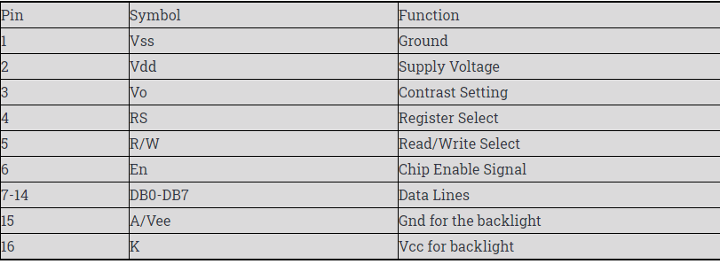
The most used ALPHANUMERIC displays are 1x16 (Single Line & 16 characters), 2x16 (Double Line & 16 character per line), 4x20 (four lines & Twenty characters per line).
The LCD requires 3 control lines that are RS, R/W & EN and 8 or 4 bit data lines. The number of data lines depends on the mode of operation. If operated in 8-bit mode then 8 data lines + 3 control lines that is 11 lines are required And if operated in 4-bit mode then 4 data lines + 3 control lines that is 7 lines are required.
 |
|
|
|
❖ When RS is low (0), the data is to be treated as a command.
❖ When RS is high (1), the data being sent is considered as text data which should be displayed on the screen.
❖ When R/W is low (0), the information on the data bus is being written to the LCD.
❖ When RW is high (1), the program is effectively reading from the LCD.
❖ The ENABLE pin is used to latch the data present on the data pins.
❖ A HIGH - LOW signal is required to latch the data.
❖ The LCD interprets and executes our command at the instant the EN line is brought low.
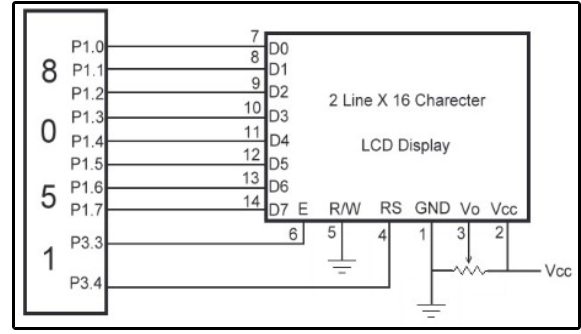
Figure 4. Interfacing of LCD with 8051.
To display a character on LCD we basically write into DDRAM. For a 2x16 LCD the DDRAM address for the first line is from 80h to 8fh & for the second line is 0c0h to 0cfh. So, to display 'H' on the 7th position of the first line then we can write at location 87h.
Data to be displayed

Command or Special Instruction

Write a program to display 'DNA TECHNOLOGY' on LCD.
ORG 0000h
CALL lcd_initialize
CALL lcd_clr
MOV A,#80h //Location from where Data is to be displayed
CALL lcd_command
MOV A,#'D'
CALL lcd_datadisplay
MOV A,#'N'
CALL lcd_datadisplay
MOV A,#'A'
CALL lcd_datadisplay
MOV A,#20h //Hex value for blank space to be displayed
CALL lcd_datadisplay
MOV A,#'T'
CALL lcd_datadisplay
MOV A,#'E'
CALL lcd_datadisplay
MOV A,#'C'
CALL lcd_datadisplay
MOV A,#'H'
CALL lcd_datadisplay
MOV A,#'N'
CALL lcd_datadisplay
MOV A,#'O'
CALL lcd_datadisplay
MOV A,#'L'
CALL lcd_datadisplay
MOV A,#'O'
CALL lcd_datadisplay
MOV A,#'G'
CALL lcd_datadisplay
MOV A,#'Y'
CALL lcd_datadisplay
Stop:
Ajmp stop.
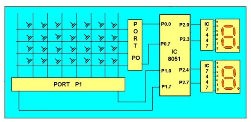
Keyboard Interfacing with 8051.
Working:
❖ The 8051 has 4 I/O ports P0 to P3 each with 8 I/O pins, P0.0 to P0.7, P1.0 to P1.7, P2.0 to P2.7, P3.0 to P3.7. Port P1 acts as an I/P port for microcontroller and port P0 as an O/P port , Port P2 is used for displaying the number of pressed keys.
❖ Make all rows of port P0 high so that it gives a high signal when key is pressed.
❖ Check if any key is pressed by scanning port P1 by checking all the columns for non- zero condition.
❖ If any key is pressed, identify which key is pressed and make one row high at a time.
❖ Initiate a counter to hold the count so that each key is counted.
❖ Check port P1 for nonzero condition. If any nonzero number is there in [accumulator], start column scanning by following step 9.
❖ Otherwise make the next row high in port P1.
❖ Add a count of 08h to the counter to move to the next row by repeating steps from step 6.
❖ If any key pressed is found, the [accumulator] content is rotated right through the carry until carry bit sets, while doing this increment count in the counter till carry is found.
❖ Move the content in the counter to display in data field or to memory location
❖ To repeat the procedures, go to step 2.
Program:
Start of main program:
To check that whether any key is pressed
Start: mov a,#00h
Mov p1,a ;making all rows of port p1 zero
Mov a,#0fh
Mov p1,a ;making all rows of port p1 high
Press: mov a,p2
Jz press ;check until any key is pressed
After making sure that any key is pressed
Mov a,#01h ;make one row high at a time
Mov r4,a
Mov r3,#00h ;initiating counter
Next: mov a,r4
Mov p1,a ;making one row high at a time
Mov a,p2 ;taking input from port A
Jnz colscan ;after getting the row jump to check
Column
Mov a,r4
Rl a ;rotate left to check next row
Mov r4,a
Mov a,r3
Add a,#08h ;increment counter by 08 count
Mov r3,a
Sjmp next ;jump to check next row
After identifying the row to check the colomn following steps are followed
Colscan: mov r5,#00h
In: rrc a ;rotate right with carry until get the carry
Jc out ;jump on getting carry
Inc r3 ;increment one count
Jmp in
Out: mov a,r3
Da a ;decimal adjust the contents of counter
Before display
Mov p2,a
Jmp start ;repeat for check next key.
Stepper Motor
▪ Stepper motors are mainly used to translate electrical pulses into mechanical movements.
▪ They are used in some disk drives, dot matrix printers. The key advantage of using a stepper motor is its position control.
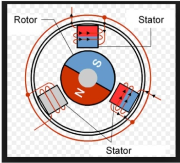
▪ Stepper motors generally have a permanent magnet shaft (rotor), and it is surrounded by a stator.
|  |
Parameters of stepper motors:
● Step Angle - The step angle is the angle at which the rotor moves when one pulse is applied as an input to the stator. This parameter determines the position of the stepper motor.
● Steps per Revolution - This is the number of step angles required for a complete revolution. The formula is 360° /Step Angle.
● Steps per Second - This parameter is used to measure the number of steps covered in each second.
● RPM - The RPM is the Revolution Per Minute. It measures the frequency of rotation. We can measure the number of rotations in one minute.
The relation between RPM steps per revolution and steps per second is
Steps per second = rpm x steps per revolution / 60
Interfacing
Port P0 of 8051 is used for connecting the stepper motor. HereULN2003 is used. This is basically a high voltage, high current Darlington transistor array. Each ULN2003 has seven NPN Darlington pairs. It can provide high voltage output with common cathode clamp diodes for switching inductive loads.
The Unipolar stepper motor works in three modes.
● Wave Drive Mode: In this mode, one coil is energized at a time. So all four coils are energized one after another. This mode produces less torque than full step drive mode.

Full Drive Mode: In this mode, two coils are energized at the same time. This mode produces more torque. Here the power consumption is also high.

Half Drive Mode: In this mode, one and two coils are energized alternately. At first, one coil is energized then two coils are energized. This is basically a combination of wave and full drive mode. It increases the angular rotation of the motor.
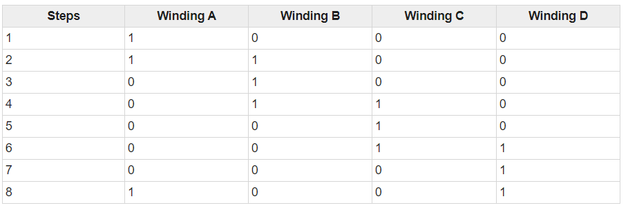
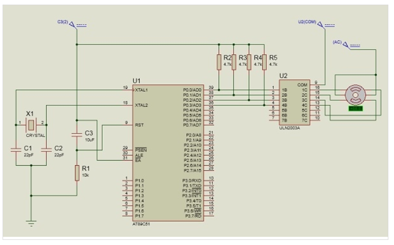
Interfacing Stepper Motor with 8051
Program:
Main : MOV A, # 0FF H ; Initialization of Port 1
MOV P1, A ;
MOV A, #77 H ; Code for the Phase 1
MOV P1, A ; ACALL DELAY ; Delay subroutine
MOV A, # BB H ; Code for the Phase II
MOV P1, A ;
ACALL DELAY ; Delay subroutine.
MOV A, # DD H ; Code for the Phase III
MOV P1, A ; ACALL DELAY ;
MOV A, # EE H ; Code for the Phase 1
MOV P1, A ;
ACALL DELAY ; Delay subroutine
SJMP MAIN; Keep the motor rotating continuously.
DELAY Subroutine
MOV R4, #0FF H ; Load R4 with FF
MOV R5, # 0FF ; Load R5 with FF
LOOP1: DJNZ R4, LOOP1 ; Decrement R4 until zero,wait
LOOP2: DJNZ R5, LOOP2 ; Decrement R5 until zero,wait
RET ; Return to main program .
This is a bidirectional DC motor that changes its direction automatically after a pre-set amount of time. AT89S51 is the microcontroller used here and L293 forms the motor driver.
The circuit diagram is shown below.
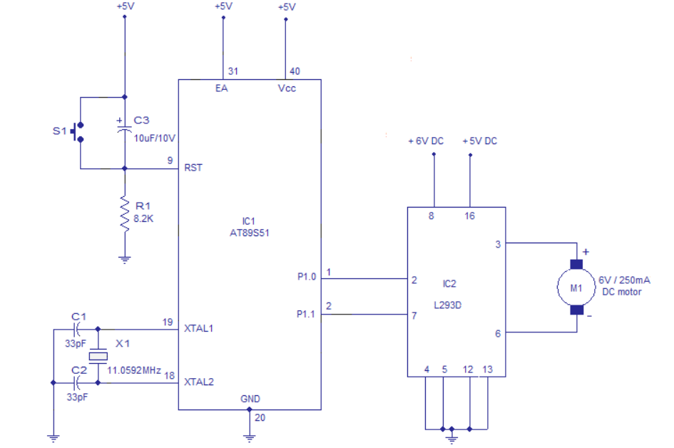
In the circuit components R1, S1 and C3 forms a debouncing reset circuitry. C1, C2 and X1 are related to the oscillator. Port pins P1.0 and P1.1 are connected to the corresponding input pins of the L293 motor driver.
The motor is connected across output pins 3 and 6 of the L293. The software is written that the logic combinations of P1.0 and P1.1 control the direction of the motor.
Initially when power is switched ON, P1.0 will be high and P1.1 will be low. This condition is maintained for a preset amount of time (around 1S) and for this time the motor will be running in the clockwise direction. Then logic of P1.0 and P1.1 are swapped and this condition is also maintained for the same duration. This makes the motor run in the anti- clockwise direction for the same duration and the entire cycle is repeated.
ORG 00H // initial starting address
MAIN: MOV P1,#00000001B // motor runs clockwise
ACALL DELAY // calls the 1S DELAY
MOV P1,#00000010B // motor runs anti clockwise
ACALL DELAY // calls the 1S DELAY
SJMP MAIN // jumps to label MAIN for repaeting the cycle
DELAY: MOV R4,#0FH
WAIT1: MOV R3,#00H
WAIT2: MOV R2,#00H
WAIT3: DJNZ R2,WAIT3
DJNZ R3,WAIT2
DJNZ R4,WAIT1
RET
END
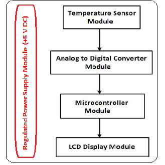
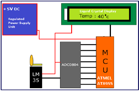
In case of temperature the Celsius and Fahrenheit scale thermometer displays the ambient temperature through a LCD display.
This consists of two sections:
▪ One senses the temperature. The temperature sensor is LM 35.
▪ The other converts the temperature value into a suitable number in Celsius scale by ADC0804.
The temperature is sensed in Celsius scale and converted into Fahrenheit scale temperature by using Celsius to Fahrenheit conversion formulae.
Process
Circuit Diagram
Interfacing of Temperature sensor with microcontroller
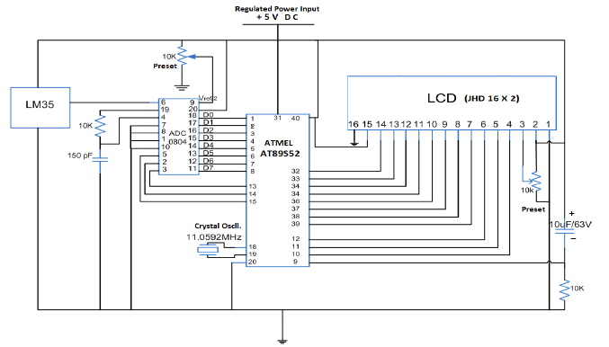
- The temperature sensor used is LM35. The LM 35 IC generates a 10mV variation in its output voltage for every degree Celsius change in temperature. The output of the temperature sensor is analog in nature.
- Hence, there is a need for an analog to digital converter to convert the analog input to its equivalent binary output.
- The ADC 0804 is the analog to digital converter IC. It is a single channel converter that converts the analog input up to a range of 5V into its equivalent 8-bit binary output.
- The step size is defined by the voltage applied at Vref/2 pin of the ADC IC.
For example, if the voltage at Vref/2 pin is set to 1.28V then ADC step size will be 10 mV. Similarly, if the input voltage is 1V the equivalent binary output of ADC will be 1000 or 0110, 0100 in binary.
- For every 10mV rise of input voltage the 8-bit binary output of ADC is incremented by one. Different step size can be selected by changing the voltage input to Vref/2 pin.
- The step size of ADC is calibrated by using a preset to match the actual temperature.
- Once ADC is calibrated it provides the correct output.
- The binary output of ADC is fed parallel to the port of the microcontroller. The microcontroller reads the input through ADC and displays its corresponding decimal value on the LCD which indicates temperature.
Program:
ORG 00H
MOV P1,#11111111B // initializes P1 as input port
MOV P0,#00000000B // initializes P0 as output port
MOV P3,#00000000B // initializes P3 as output port
MOV DPTR,#LABEL // loads the address of "LABEL" to DPTR
MAIN: MOV R4,#250D // loads register R4 with 250D
CLR P3.7 // makes Cs=0
SETB P3.6 // makes RD high
CLR P3.5 // makes WR low
SETB P3.5 // low to high pulse to WR for starting conversion
WAIT: JB P3.4,WAIT // polls until INTR=0
CLR P3.7 // ensures CS=0
CLR P3.6 // high to low pulse to RD for reading the data from ADC
MOV A,P1 // moves the digital output of ADC to accumulator A
MOV B,#10D // load B with 10D
DIV AB // divides the content of A with that in B
MOV R6,A // moves the quotient to R6
MOV R7,B // moves the remainder to R7
DLOOP:SETB P3.2 // sets P3.2 which activates LED segment 1
MOV A,R6 // moves the quotient to A
ACALL DISPLAY // calls DISPLAY subroutine
MOV P0,A // moves the content of A to P0
ACALL DELAY // calls the DELAY subroutine
CLR A // clears A
MOV A,R7 // moves the remainder to A
CLR P3.2 // deactivates LED segment 1
SETB P3.1 // activates LED segment 2
ACALL DISPLAY
MOV P0,A
ACALL DELAY
CLR A
CLR P3.1 // deactivates LED segment 2
DJNZ R4,DLOOP // repeats the loop "DLOOP" until R4=0
SJMP MAIN // jumps back to the main loop
DELAY: MOV R3,#255D // produces around 0.8mS delay
LABEL1: DJNZ R3,LABEL1
RET
DISPLAY: MOVC A,@A+DPTR // converts A's content to corresponding digit drive pattern
RET
LABEL: DB 3FH // LUT (look up table) starts here
DB 06H
DB 5BH
DB 4FH
DB 66H
DB 6DH
DB 7DH
DB 07H
DB 7FH
DB 6FH
END
References:
❖ 8051 Microcontroller: An Applications Based Introduction Book by David Calcutt, Frederick J. Cowan, and Hassan Parchizadeh
❖ 8051 Microcontrollers: Internals, Instructions, Programming, and Interfacing Book by Subrata Ghoshal
❖ C and the 8051: Building efficient applications Book by Thomas W. Schultz
❖ MICROCONTROLLER Book by V. Udayashankara
❖ The 8051/8052 Microcontroller: Architecture, Assembly Language, and Hardware Interfacing Book by Craig Steiner