Unit - 1
Introduction MOSFET
The MOSFET transistor is a semiconductor device which is widely used for switching and amplifying electronic signals in the electronic devices.
The MOSFET is a four-terminal device with source(S), gate (G), drain (D) and body (B) terminals. The body of the MOSFET is frequently connected to the source terminal making it a three- terminal device like field effect transistor.
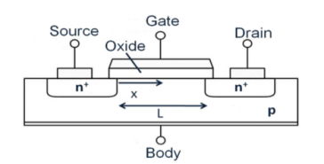
Figure 1. MOSFET
The MOSFET works by varying the width of a channel along which charge carriers flow (electrons or holes). The charge carriers enter the channel at source and exit via the drain.
The width of the channel is controlled by the voltage on an electrode is called gate which is located between source and drain. It is insulated from the channel near an extremely thin layer of metal oxide.
The MOS capacity present in the device is primary.
The MOSFET can function in two ways
- Depletion Mode
- Enhancement Mode
Depletion Mode:
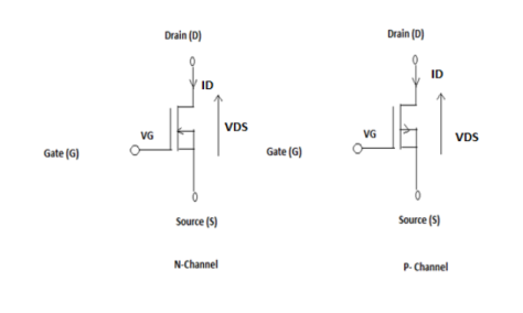
Figure 2. Depletion mode
When there is no voltage on the gate, the channel displays maximum conductance. As the voltage on the gate is either positive or negative, the channel conductivity decreases.
Enhancement Mode
When there is no voltage on the gate the device does not conduct. More is the voltage on the gate, the better the device can conduct.
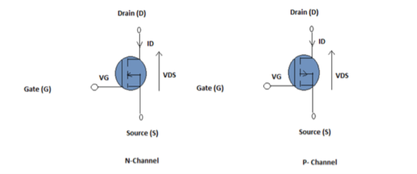
Figure 3. Enhancement mode
Working:
The working of MOSFET depends upon the MOS capacitor. The MOS capacitor forms main part of MOSFET. The semiconductor surface at the below oxide layer is located between the source and drain terminal
- It can be inverted from p-type to n-type by applying a positive or negative gate voltage respectively. When we apply the positive gate voltage the holes present under the oxide layer with a repulsive force and holes are pushed downward with the substrate.
- The depletion region populated by the bound negative charges which are associated with the acceptor atoms. The electrons reach channel is formed.
- The positive voltage also attracts electrons from the n+ source and drain regions into the channel.
- Now, if a voltage is applied between the drain and source, the current flows freely between the source and drain and the gate voltage controls the electrons in the channel. Instead of positive voltage if we apply negative voltage, a hole channel will be formed under the oxide layer.
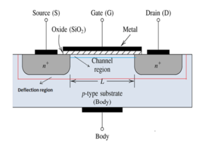
Figure 4. MOSFET construction
P-channel MOSFET
- The P- Channel MOSFET has a P- Channel region between source and drain. It is a four terminal device such as gate, drain, source, body. The drain and source are heavily doped p+ region and the body or substrate is n-type.
- The flow of current is positively charged holes. When we apply the negative gate voltage, the electrons present under the oxide layer are pushed downward into the substrate with a repulsive force.
- The depletion region populated by the bound positive charges which are associated with the donor atoms. The negative gate voltage also attracts holes from p+ source and drain region into the channel region.
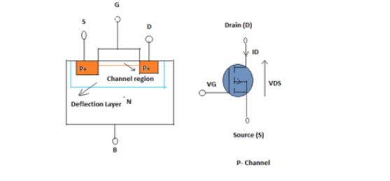
Enhanced mode
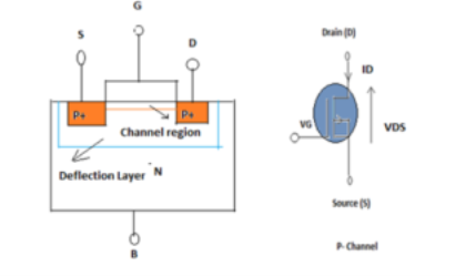
Depletion mode
Figure 5. P-channel MOSFET
N- Channel MOSFET:
- The N-Channel MOSFET has a N- channel region between source and drain It is a four terminal device such as gate, drain, source, body. This type of MOSFET the drain and source are heavily doped n+ region and the substrate or body is P- type. The current flows due to the negatively charged electrons.
- When we apply the positive gate voltage the holes present under the oxide layer pushed downward into the substrate with a repulsive force. The depletion region is populated by the bound negative charges which are associated with the acceptor atoms. The electrons reach channel is formed.
- The positive voltage also attracts electrons from the n+ source and drain regions into the channel. Now, if a voltage is applied between the drain and source the current flows freely between the source and drain and the gate voltage controls the electrons in the channel.
- Instead of positive voltage if we apply negative voltage a hole channel will be formed under the oxide layer.
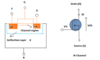
Enhancement mode
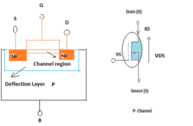
Depletion mode
Figure 6. N-channel MOSFET
Key takeaway
- The channel width of the MOSFET varies with the flow of the charge carriers and this is the phenomenon behind its working.
- Through the source terminal the carriers enter the channel and flow towards the drain.
- The gate terminal controls the channel width.
- It is insulated from the channel near an extremely thin layer of metal oxide.
The MOSFET threshold voltage, VGS(th) is the voltage between the gate and source which is required to turn on the MOSFET. In other words, if VGS is as high as the threshold voltage, the MOSFET turns on.
Electrical characteristics (Ta = 25oC)
Parameter | Symbol | Conditions | Values | Unit | ||
Min. | Typ. | Max. | ||||
Drain-Source breakdown voltage | V(BR)DSS | VGS = 0V, ID = 1mA | 600 | - | - | V |
Zero-gate voltage drain current | IDSS | VDS = 600 V, VGS = 0V Tj = 25oC Tj = 125oC |
- - |
- - |
100 1000 | μA |
Gate - Source leakage current | IGSS | VGS = ±20V, VDS = 0V | - | - | ±100 | NA |
Gate threshold voltage | VGS(th) | VDS = 10V, ID = 1 mA | 3 | - | 5 | V |
Static drain - source on - state resistance | RDS(on)*5 | VGS = 10V, ID = 1.5A Tj = 25oC Tj = 125oC |
- - |
0.90 1.36 |
0.98 - |
Ω |
Gate resistance | RG | f = 1MHz, open drain | - | 3.3 | - | Ω |
The blue box surrounds information on VGS(th), and the conditions column indicates that conditions are VDS = 10 V and ID = 1 mA. Under these conditions, and at Ta = 25℃, VGS(th) have minimum and maximum values of 3 V and 5 V.
In other words, as VGS is raised, the MOSFET begins to turn on and when ID = 1 mA, the value of VGS is between 3 V and 5 V inclusive; this value is VGS(th).
Temperature Characteristics of VGS(th) and ID-VGS
From the initial graph showing the ID-VGS characteristic, the VGS(th) for the MOSFET can be read off. The condition VDS = 10 V matches the stipulated condition. When ID is 1 mA, VGS is equal to VGS(th), and so the VGS when the curve for Ta = 25℃ intersects the 1 mA (0.001 A) line is approx. 3.8 V. The datasheet does not indicate a representative or typical value (indicated by "Typ"), and we see from the graph that the Typ value for VGS(th) is about 3.8 V. The graph value can in essence be regarded as the Typ value.
Next, we consider the ID-VGS characteristic. As the specification value for VGS(th), the value when ID = 1 mA is used, but in actual use, a 4 A MOSFET is unlikely to be used with ID at only 1 mA. For example, when an ID of 1 A at Ta = 25℃ is required, we see from the graph that the VGS is about 5.3 V.
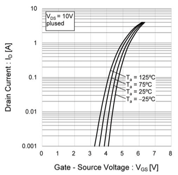
Fig 7: I-V curve
From the graph of the ID-VGS temperature characteristic, at high temperatures there is a tendency for ID to increase if VGS is constant. Taking as an example the previous condition that ID = 1 A at Ta = 25℃, at Ta = 75℃, an ID of about 1.5 A can be passed, and so the conditions of use must be considered carefully.
Returning to the gate threshold voltage, the temperature characteristic of VGS(th) is shown in a graph. As was seen from the ID-VGS graph, we see that at 25℃, VGS(th) is approx. 3.8 V. The temperature in this graph is Tj, but as indicated by the term "pulsed", the data was obtained in pulsed tests, and it is permissible to assume that Tj≈ Ta ≈ 25℃.
It is seen that the temperature characteristic is such that at high temperatures, VGS(th) tends to decline. This indicates that as the temperature rises, because VGS(th) declines, a larger ID can flow at a lower VGS. In other words, and as would be expected, this matches the ID-VGS temperature characteristic.
VGS(th) can be used to estimate Tj. The VGS(th) temperature characteristic is linear, and so a proportionality coefficient can be calculated, and the increase in temperature can be calculated from the amount of change in VGS(th).
The resistance of the channel is inversely proportional to its width-to-length ratio; reducing the length leads to decreased resistance and hence higher current flow. Thus, channel-length modulation means that the saturation-region drain current will increase slightly as the drain-to-source voltage increases.


Where

This is a first-order approximation that is reasonably accurate for FETs with channel length greater than, say, 2 µm. As the channel length decreases, so-called “short-channel effects” become more influential, and thus the above expression becomes less valid.
The short-channel effects are attributed to two physical phenomena:
1. The limitation imposed on electron drift characteristics in the channel,
2. The modification of the threshold voltage due to the shortening channel length.
In particular five different short-channel effects can be distinguished:
1. Drain-induced barrier lowering and punch through
2. Surface scattering
3. Velocity saturation
4. Impact ionization
5. Hot electrons
The drain terminal (D) of the MOSFET is connected to the supply voltage VS via the drain resistor RD while its source terminal (S) is grounded. It has an input voltage Vi applied at its gate terminal (G) while the output Vo is drawn from its drain.
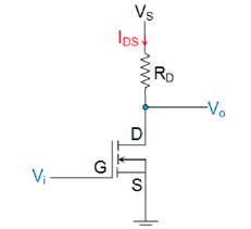
Figure 8. n-channel Enhancement MOSFET functioning as a switch
- When Vi = 0V, which means the gate terminal of the MOSFET is left unbiased. As a result, the MOSFET will be OFF and operates in its cut-off region wherein it offers a high impedance path to the flow of current which makes the IDS almost equivalent to zero.
- As a result, even the voltage drop across RD will become zero due to which the output voltage Vo will become almost equal to VS.
When Vi >VT under this condition, the MOSFET will start to conduct and if the VS provided is greater than the pinch-off voltage VP of the device then the MOSFET starts to operate in its saturation region. - The device will offer low resistance path for the flow of constant IDS, almost acting like a short circuit. As a result, the output voltage will be pulled towards low voltage level, which will be ideally zero.
Thus, the output voltage alters between VS and zero depending on whether the input provided is less than or greater than VT, respectively. Thus, it can be concluded that MOSFET can be made to function as electronic switches when made to operate between cut-off and saturation operating regions.
Due to their structure, MOSFETs have a parasitic capacitance, as indicated in the diagram below. The diagram below is for an example of an N-channel MOSFET, but the situation is much the same for P-channel devices. In the power MOSFETs we are here considering that handle large amounts of power, the parasitic capacitance must be regarded as a parameter that limits the usage frequency and switching speed.
The drain and source of a MOSFET are insulated from the gate by the gate oxide film. A PN junction is formed between the drain and source with substrate intervening, and a parasitic ("body") diode is present.
The gate-source capacitance Cgs and gate-drain capacitance Cgd in the diagram below are determined by the capacitance of the gate oxide film. The drain-source capacitance Cds is the junction capacitance of the parasitic diode.

Fig 9: gate-source capacitance
The three parameters Ciss, Coss, Crss appearing on MOSFET data sheets in general relate to these parasitic capacitances. On data sheets which provide separate descriptions of static characteristics and dynamic characteristics, these are classified as dynamic characteristics. These are important parameters affecting switching performance.
Ciss is the input capacitance, and is the capacitance obtained by totaling the gate-source capacitance Cgs and the gate-drain capacitance Cgd; it is the capacitance of the MOSFET as a whole, as seen from the input. This capacitance must be driven (charged) in order to cause the MOSFET to operate, and so is a parameter of importance when studying the drivability of an input device or input losses. Qg is the amount of charge necessary to drive (charge) Ciss.
Coss is the output capacitance, obtained by adding the drain-source capacitance Cds and the gate-drain capacitance Cgs, and is the total capacitance on the output side. If Coss is large, a current arising due to Coss flows at the output even when the gate is turned off, and time is required for the output to turn off completely.
Crss is the gate-drain capacitance Cgd itself, and is called the feedback capacitance or the reverse transfer capacitance. If Crss is large, the rise in drain current is delayed even after the gate is turned on, and the fall in current is delayed after the gate is turned off. In other words, this parameter greatly affects switching speed. Qgd is the charge amount necessary to drive (charge) Crss.
These capacitances exhibit a dependence on the drain-source voltage VDS. As indicated in the graph, there is a tendency for capacitance values to be reduced as VDS is increased.
- SPICE (Simulation Program with Integrated Circuit Emphasis) is a general-purpose circuit simulator which is used very widely both in the microelectronics industry and in educational institutions as an essential computer-aided design (CAD) tool for circuit design.
- SPICE has four built-in MOSFET models: LEVEL 1 (MOS1) is described by a square-law current-voltage characteristic, LEVEL 2 (MOS2) is a detailed analytical MOSFET model, LEVEL 3 (MOS3) is a semi-empirical model, and BSIM is the Berkley Short Channel model for IGFET.
- The level (type) of the MOSFET model to be used in a particular simulation task is declared on the MODEL statement.
- Both MOS2 and MOS3 include second-order effects such as the short-channel threshold voltage, sub-threshold conduction, scattering-limited velocity saturation, and charge-controlled capacitances.
LEVEL 1
- The equivalent circuit structure of the NMOS LEVEL 1 model, which is the default MOSFET model in SPICE, is shown in figure below
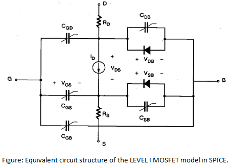
Fig1 0: MOSFET model
- The LEVEL 1 model is the simplest current-voltage description of the MOSFET
- The equations used for the LEVEL 1 n-channel MOSFET model in SPICE are as follows.


Five electrical parameters completely characterize this model: k’, VT0, λ, γ and |2ФF|
- LEVEL 1 model is not very precise due to gradual channel approximation.
- It is used in the derivation of model equation is too approximate and the number of fitting parameters is too small.
- It is useful for quick and rough estimate of circuit performance without much accuracy.
LEVEL 2
- To obtain a more accurate model for the drain current, it is necessary to eliminate some of the simplifying assumptions made in the original GCA analysis. Specifically, the bulk depletion charge must be calculated by taking into account its dependence on the channel voltage.
- Solving the drain current equation using the voltage-dependent bulk charge term, the following current-voltage characteristics can be obtained:

- Here, VFB denotes the flat-band voltage of the MOSFET. The saturation condition is reached when the channel (inversion) charge at the drain end becomes equal to zero. From this definition, the saturation voltage VDSAT can be calculated as


- The zero-bias threshold voltage VTO corresponding to the LEVEL 2 model can be calculated as follows:

- LEVEL 2 supports additional effects as listed above
- If all model parameters in model 2 are specified by the user then greatest level of complexity will be obtained.
- In such cases it requires large amount of CPU time for calculations.
LEVEL 3
- In this level we are getting the same approximate as level 2 but CPU time is significantly less and number of iterations are also fewer.
- However disadvantage is that it leads to complexity while calculating sum of its model parameters.
LEVEL 4 – BSIM
- This level is analytically simple.
- It is based on small number of parameters which are normally extracted from experimental data.
- One of the most popular models used in micro electronic industry due to its accuracy & efficiency.
- It is widely used to accurately model the electrical behavior of sub-micron MOSFETs that are manufactured with various sub-micron CMOS fabrication processes.
Here we divide all of the models in to three categories:
Professional physical models Professional table-based models Simple physical models
Professional Physical Models These models have been developed based on the accurate study of the related physical phenomena. In nanometer scale MOS technologies, these phenomena’s, especially short channel and quantum effects, are very complicated and hence such models are very complicated.
Table-Based Models As the MOS technology goes to nanometer regime, capturing the new physical phenomena’s makes the professional physical based models more and more complicated. Such complicated models are computationally expensive and a greatly influence the simulation run time, so that up to 80% of the run time is consumed to model evaluations. On the other hand simple physical models have not enough accuracy for final design evaluation and optimization
Simple Physical Models Due to their complexity, professional MOS models cannot be used in the simple individual design tools. Simple Physical Models Due to their complexity, professional MOS models cannot be used in the simple individual design tools.
Layout Design Rules
The design rules primary address two issues:
1. The geometrical reproduction of features that can be reproduced by the mask making and lithographical process, and
2. The interaction between different layers.
There are primarily two approaches in describing the design rules.
1. Linear scaling is possible only over a limited range of dimensions.
2. Scalable design rules are conservative. This, results in over dimensioned and less dense design.
3. This rule is not used in real life.
1. Scalable Design Rules (e.g., SCMOS, λ-based design rules):
In this approach, all rules are defined in terms of a single parameter λ. The rules are so chosen that a design can be easily ported over a cross section of industrial process, making the layout portable. Scaling can be easily done by simply changing the value of. The key disadvantages of this approach are:
2. Absolute Design Rules (e.g., μ-based design rules): In this approach, the design rules are expressed in absolute dimensions (e.g., 0.75μm) and therefore can exploit the features of a given process to a maximum degree. Here, scaling and porting is more demanding, and has to be performed either manually or using CAD tools. Also, these rules tend to be more complex especially for deep submicron.
The fundamental unity in the definition of a set of design rules is the minimum line width. It stands for the minimum mask dimension that can be safely transferred to the semiconductor material. Even, for the same minimum dimension, design rules tend to differ from company to company, and from process to process. Now, CAD tools allow designs to migrate between compatible processes.
Layer Representations
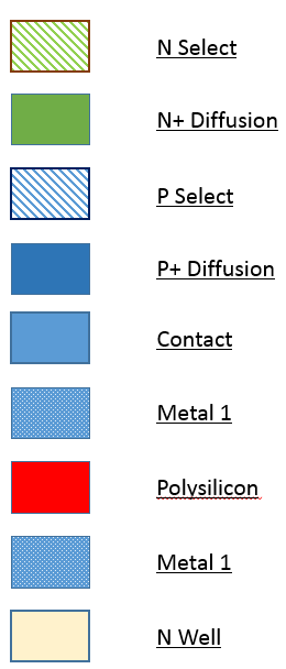
With increase of complexity in the CMOS processes, the visualization of all the mask levels that are used in the actual fabrication process becomes inhibited. The layer concept translates these masks to a set of conceptual layout levels that are easier to visualize by the circuit designer. From the designer's viewpoint, all CMOS designs have the following entities:
- Two different substrates and/or wells: which is p-type for NMOS and n-type for PMOS.
- Diffusion regions (p+ and n+): which defines the area where transistors can be formed. These regions are also called active areas. Diffusion of an inverse type is needed to implement contacts to the well or to substrate. These, are called select regions.
- Transistor gate electrodes: Polysilicon layer
- Metal interconnect layers
- Interlayer contacts and via layers. The layers for typical CMOS processes are represented in various figures in terms of:
- A colour scheme (Mead-Conway colours).
- Other colour schemes designed to differentiate CMOS structures.
- Varying stipple patterns
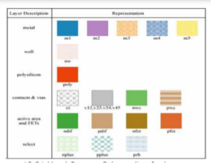
Fig 11 Mead Conway Colour coding for layers
Key takeaway
With increase of complexity in the CMOS processes, the visualization of all the mask levels that are used in the actual fabrication process becomes inhibited.
When two conductive elements on PCBA are close to each other and at different voltage levels they form an intrinsic and typically unwanted capacitor. This is known as the parasitic capacitive effect.
The two elements may be two-component pins, two traces, a pad and a trace, a pad, and a pin, or any other two conductive elements on the board. As the intrinsic capacitor plates have a charge differential there is an opportunity for current flow. Now, current does not flow through the capacitor instead an electrical charge differential is accumulated between the plates. As this charge differential increases, a corresponding decrease in electron flow is available for the desired signal path that negatively impacts signal integrity.
Effects Of Parasitic Capacitance
- Crosstalk
- Unintended feedback between output and input for components; such as amplifiers.
- Noise
- Formation of resonant circuits with stray inductance
Key takeaways:
Parasitic capacitance or stray capacitance is an unavoidable and usually unwanted capacitance that exists between the parts of an electronic component or circuit simply because of their proximity to each other.
References:
1. Fundamentals of Modern VLSI Devices Book by Tak H. Ning and Yuan Taur
2. Introduction to VLSI systems Book by Carver Mead
3. VLSI physical design automation Textbook by Sadiq Sait
4. CMOS Digital Integrated Circuits Book by Sung-Mo Kang and Yusuf Leblebici