UNIT 2
MICROWAVE ENGINEERING
Introduction
The most important microwave tubes are the linear - beam tubes or O - type tubes like the two cavity klystron and the reflex klystron.
In these tubes, electrons receive potential energy from the dc beam voltage before they arrive in the microwave interaction region and this energy is converted into their kinetic energy. In the microwave interaction region, the electrons are either accelerated or decelerated by the microwave field and then bunched as they drift down the tube. The bunched electrons induce current in the output structure. The electrons then give up their kinetic energy to the microwave fields and are collected by the collector. O - type tubes are suitable for amplification as well as oscillations.
A two cavity klystron amplifier consists of a cathode, focusing electrodes, two buncher grids separated by a very small distance forming a gap of two catcher grids with a small gap followed by a collector. The cavity close to the cathode is called the buncher cavity or input cavity, which velocity modulates the electron beam and the other cavity close to the collector is called the catcher cavity or the output cavity as it catches energy from the bunched electron beam.
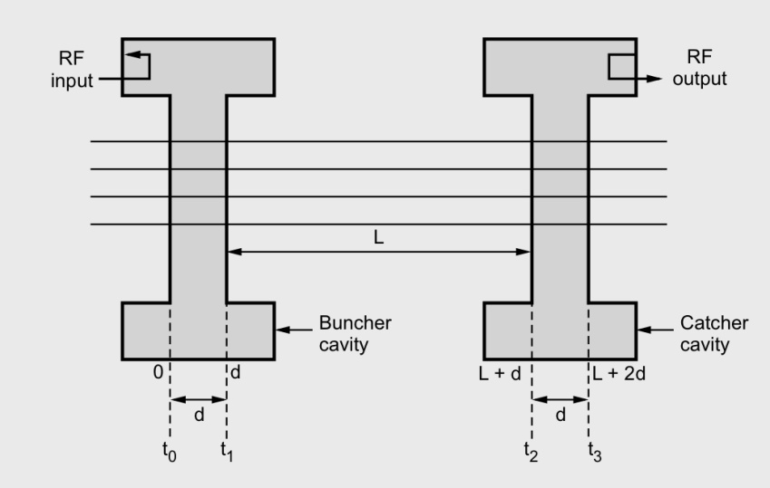
The bunching process in two cavity klystrons is not perfect since large number of electrons which are out of phase, arrive at the catcher cavity between bunches. So the maximum gain is about 20 dB. To obtain higher gain, more than two cavities are employed. This arrangement is called Multicavity Klystron.
The output of each tube is connected to the input of succeeding one. Such an arrangement is called cascading of cavity and maximum seven cavities can be used. The intermediate cavities act as a buncher, producing more complete bunching and hence including more RF voltage which improves efficiency and power gain.
By using multicavity, the bandwidth can be increased and the increase in bandwidth decreases the gain.
The broadband klystron amplifiers are used in UHF klystrons for television transmitter output tubes. In satellite earth station transmitters, the UHF klystrons are used as power amplifiers at 6 GHz.
Two and multicavity klystrons are power amplifiers and not oscillators. For use as an oscillator, reflex klystrons are used.
A reflex klystron requires a single resonant cavity and replaces the collector with a repeller electrode. The electrode is biased with negative potential to repel the electrons and the bunching of the electrons occur in the vicinity of the repeller electrode. Bunched electrons returning to the cavity form an internal positive feedback that excites the cavity into self oscillations.
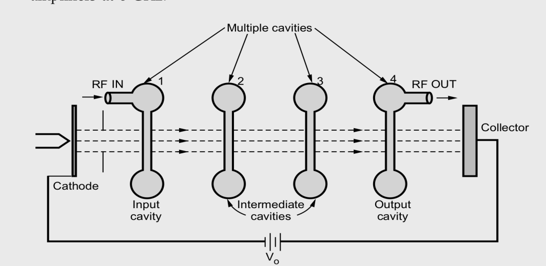
MULTICAVITY KLYSTRON AMPLIFIER
The Reflex Klystron is a single cavity velocity modulated tube in which single cavity does the functions of both the buncher and cavity resonators. It consists of an anode cavity resonator a filament surrounded by cathode, an electron gun and an electrode also called reflector electrode. Reflector electrode is placed at a short distance from resonator grid and is at negative potential with respect to the cathode. The electron beam is modulated when passed through the anode resonant cavity. The electrons travel towards the repeller electrode after passing through the gap in the cavity. Because of the high negative field, the electrons never reach the reflector elecrode and are returned back towards the gap and on their return journey, the electrons give more energy to the gap and oscillations are sustained.
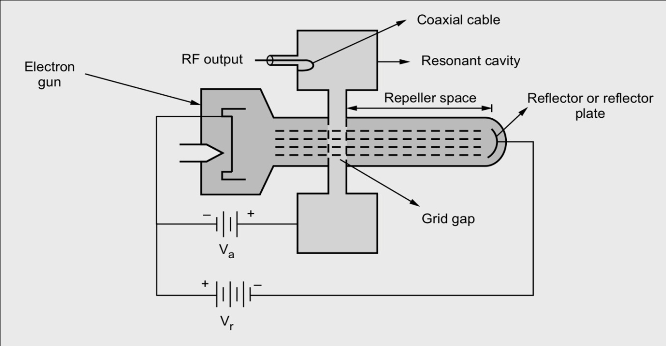
REFLEX KLYSTRON
In the operation of reflex Klystron three power sources are required:
- Filament power.
- Positive resonator voltage or beam voltage which is used to accelerate the electrodes through the grid gap of resonant cavity.
3. Negative repeller voltage used to push the electrons back to resonator
Grids.
The electrons are focused into a beam by electrostatic fields set up by the resonator potential . The resonator potential also causes the resonant cavity to begin oscillations at its natural frequency when the tube is energized. These oscillations causes the RF voltage across the grid gap of the cavity that changes the direction of electrostatic field and affect the electrons in the beam as they pass through the grid gap.
When gap voltage is zero, the electron passes through the gap and is known as reference electron i.e. . Reference electron , is unaffected by the gap voltage and moves towards the reflector electrode. This electron gets reflected by the negative potential of the reflector electrode. It returns back to the gap.
The electron which passes through the gap before the reference electron, , is known as early electron i.e.. This electron exhibits the maximum positive potential and accelerated moves with great velocity and it penetrates deep into repeller space. In return journey from reflector electrode to grid gap, the takes greater time than because of more penetration into repeller space. The electron which passes through the gap after the reference electron is known as the late electron . It exhibits maximum negative potential on it and moves with the retarding velocity. The return journey time of is much shorter than the andelectron because of the less penetration into the repeller space. The late electron 'catches up with the reference electron and early electron to form a bunch. The bunching of electrons occur once per cycle centred around the reference electron and these bunches transfer the maximum energy to grid gap. Due to this energy of grid gap, the oscillations are sustained in the cavity resonator.
The time taken by the electrons to travel towards the reflector electrode and return back to the grid gap is known as the transit time. In case of reflex Klystron the optimum transit time is most important factor for oscillation to be sustained.
The most optimum departure time is centered around the reference electron which is at 180º phase difference from the sine wave voltage across resonator gap. The cavity resonator gives up energy thus accelerating the electrons and gains energy thus retarding the electrons. When the positive gap voltage will be applied to the maximum retardation to the electrons then it is the best time for electrons to return towards the gap. This causes electrons to fall through a negative voltage between gap grids and giving up maximum amount of energy to the gap which is at the 90º phase difference from the sine wave of gap voltage. The reference electrons must remain in the reflecting field space for a minimum time of 3/4 cycle of grid field for maximum energy transfer. The reflex Klystron will continue to oscillate if the electrons remain in the repeller field longer than 3/4 cycle.
The optimum transit time should be T=n+ 3/4 where n is any integer. The difference in transit time (such as 3/4, 7/4, 11/4) causes the change in performance characteristics of the reflex Klystron. The reflex Klystron operates in different modes for different characteristics caused by transit time. The modes are, Mode1 : Reflex Klystrons operate in this mode when the repeller voltage produces an electron transmit time of 3/4 cycle.
Mode 2 : Reflex Klystron operates in this mode when repeller voltage produces an electron transit time of 7/4 cycle.
Mode 3 : This mode is obtained when the repeller voltage produces an electron transit time of 11/4 cycles. The choice of mode is determined by the difference of power available from each mode. The mode 1 gives the larger output power but voltage requirement is also higher which affects the efficiency of the reflex Klystron. So mode 2 and mode 3 are most widely used in practical.
Characteristics of Reflex Klystron :
The performance characteristics of reflex Klystron are as follows :
1) Operating frequency range: 4 GHz to 200 GHz.
2) Output power: 10 mW to 2.5 W.
3) Efficiency: 20%
4) Bandwidth: " 25 MHz
Applications of klystrons:
- Pump oscillator for parametric amplifiers.
2. Frequency-modulated oscillator in portable microwave links.
3. Local oscillator in microwave receivers.
4. Signal source in microwave generators.
The magnetron is a self contained microwave oscillator that operates differently from linear wave tubes, such as the TWT and Klystron. The magnetrons are cross field tubes in which electric and magnetic fields are perpendicular to each other, so these tubes are known as M-type microwave tubes.
Cylindrical magnetron consists of a cylindrical cathode of finite length and radius 'a' at the centre surrounded by a cylindrical anode of radius 'b'. The anode has several re-entrant cavities which are equi-spaced around the circumference. These cavities are 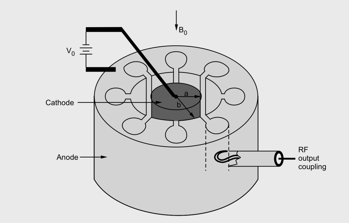
connected between anode and cathode by slots.
CYLINDRICAL MAGNETRO
The dc voltage is applied between anode and cathode. The magnetic flux density is
Maintained in positive-z direction by an electromagnet. If the dc voltage and the magnetic flux are adjusted properly then under the combined forces the electrons follow the cycloidal path between anode-cathode space. The figure below shows the cycloidal path of electrons under the balanced electric and magnetic field strength.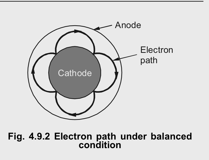
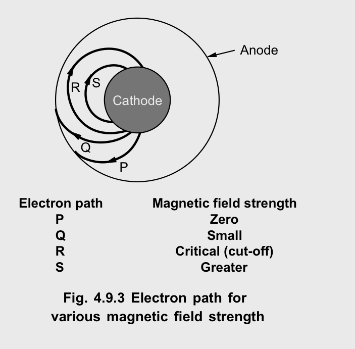
The path of electron for various magnetic field strength are shown :
The open space between cathode and anode is called the interaction space. In this space, the electric and magnetic fields interact to exert force upon the electrons. The magnetic field is usually provided by a strong permanent magnet mounted around the magnetron so that magnetic field is parallel with the axis of the cathode.
There are three types of Magnetrons 1) Negative resistance type 2) Cyclotron frequency type 3) Travelling wave or cavity type. 1. Negative Resistance Type These are useful only at the frequency less than 500 MHz. These magnetrons uses the negative resistance between two anode segments. The negative resistance magnetrons are capable of generating high power output. The length of the tube plate is limited to few centimetres. The small diameter tube is required to make the magnetron operate efficiently at microwave frequency. 2. Cyclotron Frequency Type These are useful only for frequencies greater than 100 MHz. The working of these magnetrons depends upon the synchronisation between an alternating component of electric field and periodic oscillations of electrons in the direction parallel to this field. 3. Travelling Wave or Cavity Type These magnetrons provides the oscillations of very high peak power. These are very useful in radar applications. The working of these magnetrons depend upon the interaction of electrons with a rotating electromagnetic field of constant angular velocity. We have already discussed the construction of these magnetrons. In next section we will discuss the operation of cavity magnetrons.
Working of Magnetron :
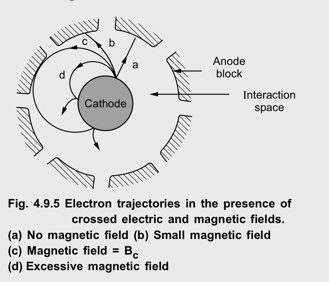
1) When there is no RF field in cavity magnetron (zero-mode): The strong electric field going from anode to cathode is created by applying the negative voltage pulse to cathode. The strong electric field causes the electrons to accelerate towards the anode after they have been accelerated by the cathode. The electron takes the energy from field when it is accelerated by electric field and moves against the electric field. An electron gives up energy to the field and slows down if it moves in the same direction as the electric field. Oscillations are sustained in the magnetron because of the acceleration and retardation of the electric and magnetic fields. In the diagram a, b c and d are four different electrons which exerts different electric and magnetic field (B = 0), the electron travels in a straight line from cathode to anode due to the radial electric field force action on it. If the magnetic field strength is increased slightly, it will exert lateral force on it and it travels from cathode to anode in a small current path (electron 'b'). As shown in the figure, the radius of the path varies directly with electron velocity and inversely proportional to the magnetic field strength. The radius is given by, R = mV/eB where ‘m’ is mass of the electron, ‘e’ is charge on the electron. When magnetic field is increased, then the electron donot reach the anode shown by path of electron 'C' in the figure and the anode current becomes zero. The magnetic field required to return electrons back to the cathode is called the critical magnetic field . If the magnetic field is made larger than the critical field the electron exerts a greater force on it and it returns back to cathode faster than the electron C, as shown by path of electron 'd' in thefigure. All such electrons may cause back heating of the cathode. This can be avoided by switching off the heater.
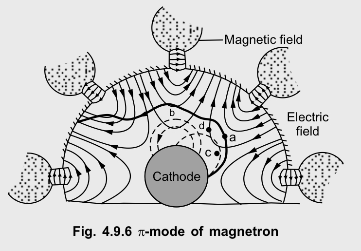
2) When the RF oscillations are present in cavity magnetron (-mode) the RF oscillations are initated due to some noise transient within the magnetron and oscillations are sustained by the device operation. When n = 4 then there is-mode of operation which is shown in Fig. 4.9.6. The anode poles are-radians apart in phase. The electron ‘a’ is seen to be slowed down in the presence of oscillations thus transferring energy from cathode to anode. The electrons which participate in transferring the energy to the RF field are called forward electrons and they are responsible for the bunching effect. The electron ' b' is accelerated by the RF field and it takes energy from the oscillations resulting in increased velocity. It bends more sharply, spends very little time in the interaction space and return
Back to the cathode, these electrons do not participate in the bunching process. The electron 'd' is slowed down and it falls back in step with electron ‘a’. This results in forward electrons like a, c, d to be confined to spokes or electron clouds. The spokes so formed in-mode rotate with an angular velocity corresponding to two poles per cycle. The process is called phase focussing effect, corresponding to a bunch of forward electrons around the reference electron ‘a’. The phase focussing effect of these forward electrons, imparts enough energy to the RF oscillations so that they are sustained.
Strapping
Due to mutual coupling, two or more identical cavities resonate at two different frequencies. The process of separating the - mode from other adjacent mode is known as strapping.
The strapping is also used to avoid the mode jumping in magnetrons. The resonant modes of magnetron are very close to each other. The weaker modes have slightly different frequency from dominant mode so there is always a possibility of mode jumping because the purity of oscillations is lost due to small difference of frequency of oscillations.
The disadvantage of strapping is that it may cause power loss in conducting rings, also at higher frequencies, it may cause power loss in conducting rings. At higher frequencies, it is very difficult to maintain the RF field within the interaction space and strapping causes the stray effects.
Frequency Pushing and Pulling
The process of change in resonant frequency of magnetron by changing the anode voltage is known as the frequency pushing. If there is a change in anode voltage, then orbital velocity of electrons will also change. Due to the change in velocity of electrons, the energy which is transferred to anode resonators is also changed and this factor results in the change of oscillation of frequency.
In magnetron, the change in load impedance causes the variations in frequency. This takes place whether these load variations are purely resistive or reactivevariations. The frequency variations due to the change in load impedances are known as the frequency pulling. To minimise the frequency variations a stabilized power supply is used.
To minimise the frequency pushing a circulator is placed before the waveguide connection at the output at the magnetron, this circulator does not allow the backward flow of energy.
Characteristics of Magnetron
The performance characteristics of magnetron is as follows :
- Efficiency : very high 40 to 70%
2. Power output : 800 kW (pulsed)
3. Operating frequency : upto 10 GHz.
Applications of Magnetron
- Magnetrons are widely used in radars with high output power.
2. In satellite and missiles for telemetry.
3. Industrial heating.
4. Microwave ovens
Basically, there are two types of BWO. The first type is known as O-type backward wave oscillator whereas the second type is the M-type or cross field type. The O-type is used as low power oscillator having a typical output of few hundred milliwatts over a frequency range of 1–15 GHz. This type of BWO is also known as Carcinotron. The M-type can produce an output of a few hundred watts in the frequency range of a few gigahertz.
It has the following major elements. Electron gun: to form and accelerate a beam of electrons.Helix, a slow wave structure: where electron beam interacts with the weak RF power to be amplified. Collector plate: to collect the electrons after release of microwave energy.
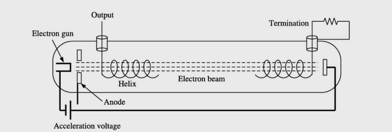
The working principle of O-type BWO is same as that of TWT. The process of oscillation in BWO is precisely same as in case of other oscillators. The electron beam is fired into the helix, whose phase velocity is equal to the beam velocity. The helix is a slow wave structure through which the electron beam passes very close to each turn of helix. Like TWT, the axial velocity of the field is reduced. The waves which travel backward on the tube, velocity modulate the beam and cause density modulation so that electrons tend to bunch. These bunches of electrons reinforce the input RF signal. The RF output obtained from BWO is a result of interaction between the electron beam and the electric field. The term backward wave is fully justified because the RF energy moves and builds up in the direction opposite to that of the electron beam and is collected from helix terminal at electron gun end of the tube. The feedback signal is due to imperfectly terminated collector end of helix. So, oscillations are maintained by the energy received from retarded electrons during their journey from input end to the collector end.
Performance Characteristics
The O-type power: 1 mW to 50 mW
Frequency range: 1–15 GHz
Achievable efficiency: 20 to 30%
Applications of BWO
The O-type backward wave oscillator is very useful as a low power active device. Frequently used as a local oscillator or as low power modulator.
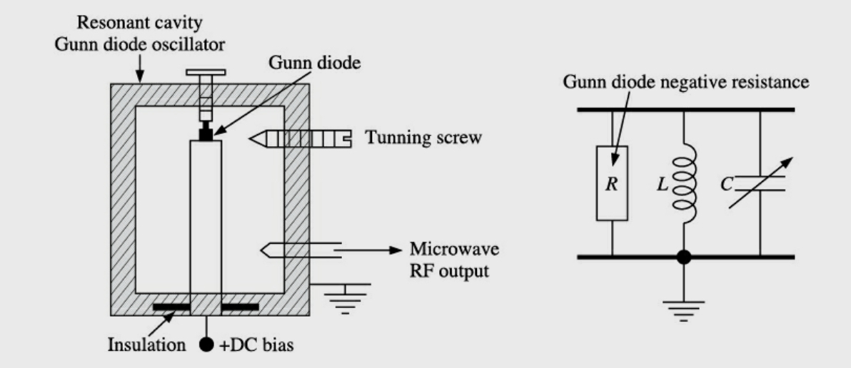
Gunn diode has a negative resistance property. To make this negative resistance diode act as an oscillator, it is required is to tune out the capacitance and a shunt load resistance not greater than negative resistance.The efficiency of Gunn diode is only a few percent. It has negative resistance of about 100 ohms in parallel with capacitance of 0.6 pF. A commercial Gunn diode will require a 9 V DC bias with an operating current of 950 mA.
Gunn diode is preferably placed in a resonant cavity which improves the efficiency and allows some variation in the operating frequency. If better electrical tuning is required, a Varactor diode is placed in the cavity at the opposite end to Gunn diode. If a sawtooth sweep voltage is applied to the Varactor diode, theGunn oscillator will be frequency modulated. The Gunn device can be very well operated as a pulsed oscillator by applying the DC bias voltage in the form of a pulse train of short rectangular pulses. If the duty cycle is low enough and very short bias pulses are applied, the peak power output will be limited only by peak current, since the thermal heating of the device will be negligible. Cavity Gunn diode oscillator can deliver power output of a few watts at 30 to 40 GHz for continuous operation and up to 200 W in pulsed operation. The heat removal from the small chip of Gunn diode is the most difficult part of its operation. Because of excessive heat, its power handling capability is limited. Commercially Gunn diodes are available for frequencies from 4 GHz to about 100 GHz.
Advantages of Gunn Oscillator
Gunn diodes have high frequency stability. They have high reliability and frequency bandwidth. Capable of broad band operation, 2: 1 VSWR for wide bandwidth range. Small size which can be very well located in any part of the circuit. Ruggedness in operation which makes this diode very stable and fit for operation in radars for long duration, deployed in field conditions. Low manufacturing cost. Low supply voltage.Noise performance of Gunn diode is on par with the klystron which is quite acceptable compared to other devices. Gunn diode has huge potential for applications in terahertz frequency band.
Disadvantages of Gunn Diode
Conventional GaAs Gunn Diodes can provide around 500 mW power at 20 GHz with 5.5% efficiency. The efficiency reduces to about 1.5% at 60 GHz and power to 50 mW. It has also been observed that at 77 GHz it gives about 0.8% efficiency. The conventional Gunn diodes have following major limitations: The device has a high turn on voltage. Low efficiency below 10 GHz. The device exhibits poor bias and poor temperature stability. Small tuning range. Spurious FM noise is very high but not bad for normal applications. The device operating current is high thus leading to more power dissipation. At millimeter frequency band, the device has lower efficiency and provides lower power.
Gunn Diode Applications
Because of high frequency capability, Gunn diodes are mainly used at microwave frequencies and above. Some of the important applications are as follows :
Used as low and medium power oscillators in microwave receivers and instruments. Majority of parametric amplifiers use Gunn diode as pump sources. The high power Gunn oscillators, ranging from 250 to 2000 mW are used as power output oscillators in low power transmitter applications such as police radars, CW Doppler radars etc.
Tunnel diode is based on the “tunneling effect” discovered by Nobel laureate Leo Esaki, hence also known as “Esaki diode”. Tunneling phenomenon is an effect that occurs when both p and n sides of the diode are heavily doped (typically 1020 atoms/ cu.cm) and the junction barrier is very small (almost of 100 Å). As per the classical physics, it is not possible for the majority charge carriers to cross the junction barrier without having kinetic energy equal to the forbidden energy gap. But Esaki with the help of quantum physics proved that probability of majority charge carriers crossing the thin barrier is quite high. For tunneling, it is required that there must be filled state
In the n-side and empty state at the p-side.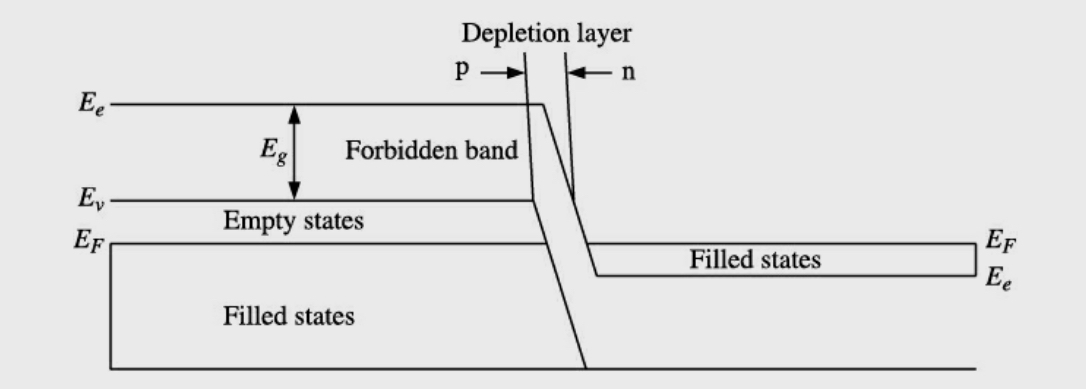
The operation of a tunnel diode can be explained in seven steps. Step 1: Due to high doping, the Fermi level goes above the conduction band in n-region and goes below the valence band in p-region of the diode. There is no current flow when the tunnel diode is zero biased.

Step 2: A small forward bias (potential barrier is still very high) creates a small forward current due to the tunneling of electrons from the conduction band in n-region to the empty states in valence band of p-region.
Step 3: With large forward bias, the diode current increases as the conduction band starts aligning with the valence band and more number of electrons start entering into the valence band.

Step 4: As the forward bias is increased, the number of electrons in the n-region that are directly opposite to the empty states in the valence bands (in terms of their energy) decreases. Therefore, decrease in the tunneling current will start.

Step 5: When more forward bias is applied, the tunnel current drops to zero but the injection current increases due to lower potential barrier.

Step 6: With further voltage increase, the tunnel diode I-V characteristic is similar to that of a regular p-n junction.

Step 7: Under reverse bias, electrons in the valence band of the p-region tunnel directly towards the empty states in the conduction side of the n-region creating large tunneling current which is directly proportional to the applied reverse voltage. Hence, I-V characteristic of a tunnel diode in reverse diode is similar to zener diode with almost zero breakdown voltage.
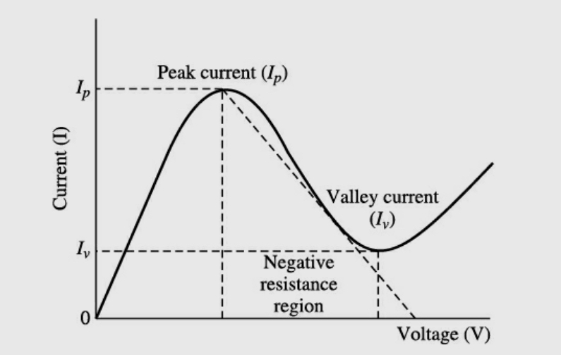
Tunnel diode is used as a microwave oscillator and an amplifier because it exhibits negative resistance region between the peak current (Ip) and valley current (minimum current) (Iv).I-V characteristic of tunnel diode with negative resistance region isshown in the figure. At point P, the negative slope of I-V curve is shown which represents the negative differential resistance. From the figure, it is clear that the current decreases (from peak to valley current) as the forward voltage increases, hence the differential negative resistance
( Rn ) can be written as:
-Rn = SV/SI
It is an acronym of IMPact ionisation Avalanche Transit Time and it is one of the improved versions of Read device. It is two terminal semiconductor negative conductance device. The principle of working of this diode is based on combination of two important phenomena. These phenomena are avalanche multiplication and transit time effects.
A schematic diagram of a basic version of IMPATT diode is shown in the figure. The structure of the device is a combination of p-n-n The diode shown in the figure has single (n ) drift region. It may have two drift regions. The junction between p and n is known as avalanche region and n region is known as drift space.
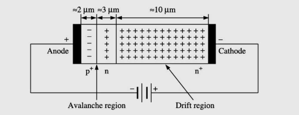
Operating Principle
The junction between p and n layers is applied with extremely high voltage gradient in the order of 400 kV/ cm. This results in very high current. Application of such high voltage across the junction of a normal diode is just not possible because it would very quickly breakdown. But IMPATT diodes are constructed in such a manner that they sustain under such conditions repeatedly. Such a high potential gradient initiates the flow of minority carriers across the junction. When RF voltage is super imposed on top of high DC voltage, electrons and holes move with very high velocity and these carriers form additional holes and electrons by knocking them out of the crystal structure. By knocking them out of crystal structure, electrons become absolutely free to move. This occurs due to the phenomenon called ‘impact ionisation’. With continuance of this process, additional carriers add up and finally snowball into an avalanche. It is to be understood well here that the original DC voltage applied to the diode was just sufficient to develop this situation however, with super imposed RF voltage on top of DC bias voltage makes the avalanche current multiplication possible in the entire period of RF cycle. It is evident from the figure that the current pulse is maximum when RF voltage across the diodegoes from zero to negative. Thus, a 90 ° phase difference between voltage and current is obtained at this point of time.
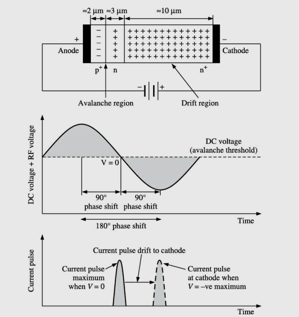
It is to be appreciated that the current pulse does not stay at the junction of the diode due to influence of reverse bias. The tendency of current pulse is always to move towards the cathode. The current flows at drift velocity across the drift space which is dependent on the presence of high DC voltage. The time taken by the current pulse to travel up to cathode depends on following two factors. (a) drift velocity and(b) thickness of drift region. By the time current pulse reaches cathode, it attains 180 ° phase difference with respect to DC and to RF voltage. 180 ° phase difference in diode is a combination of delay involved in generating avalanche current multiplication plus transit time through drift region. 90 ° phase difference is attained when the current pulse moves from maximum positive RF voltage to zero and it adds up further by 90 ° when it moves from zero voltage to maximum negative peak of RF voltage.
Advantages of IMPATT Diode
It has ability to operate at frequencies ranging from 3 to 100 GHz. This microwave diode has relatively high power capability than other diodes. Output is reliable compared to other diodes.
Disadvantages of IMPATT Diode
High noise figure due to avalanche process and high level of operating current. High level of operating current is responsible for generating shot noise in the circuit. IMPATT diode oscillators are not as good as klystron or Gunn diodes due to high level of spurious AM and FM noise.
Applications of IMPATT Diode
Pulse and CW IMPATT injection locked amplifiers. Voltage controlled IMPATT oscillators. Cavity stabilised IMPATT diode oscillators. Used extensively in low power radar systems. Used as alarms for domestic as well as industrial applications.
Reference Books
Microwave & Radar Engineering by M. Kulkarni, Umesh Publications.
Foundations of Microwave Engineering by R.F. Collins, McGraw Hill.
Microwave Principles by Reich et. Al. , Van Hestrand
Communication in Space by Jaffen, Halt Renetat Winston.