Unit-3
Field Effect Transistor
- An FET is a three-terminal amplifying device.
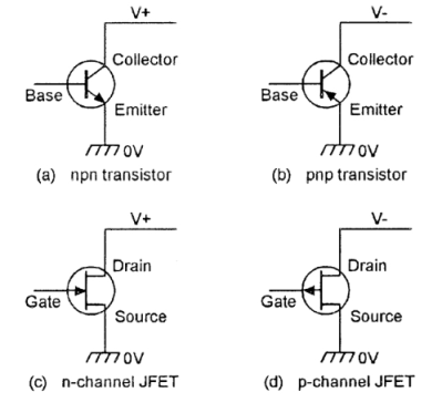
- Its terminals are source, gate, and drain, which acts respectively like emitter, base, and collector of a normal transistor.
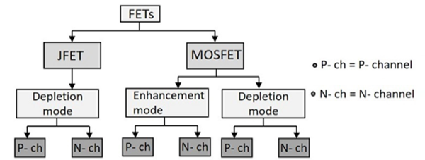
- There are two distinct families of FETs.
- The first is known as ‘junction-gate’ types of FETs or JUGFET or JFET.
- The second family is called ‘insulated-gate’ FETs or Metal Oxide Semiconductor FETs or MOSFET.
- ‘N-channel’ and ‘p-channel’ are the two versions of both types of FET.
|
Fig 1 Transistor anf JFET
Classification
|
Operation
- N-channel FET consists of n-type semiconductor material with a drain terminal and a source terminal at opposite ends.
- A p-type gate is joined in the middle section of the n-type bar, thus forming a p-n junction.
- The drain terminal is connected to a positive supply and the gate is biased at a value that is negative (or equal) to the source voltage, thus reverse-biasing the JFET’s internal p-n junction, and accounting for its very high input impedance.
- When gate = 0V, a current flow from drain to source via a conductive ‘channel’ and the n-type bar is formed.
- When gate = negative , a high resistance region is formed within the junction, thus reduces the magnitude of the drain-to-source current and width of the n-type conduction channel.
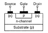
- Thus, the basic JFET passes maximum current when its gate bias is zero, and its current is reduced or ‘depleted’ when the gate bias is increased. It is thus known as a ‘depletion-type’ n-channel JFET.
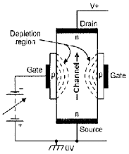
Fig 3 N-channel JFET
I-V characteristics
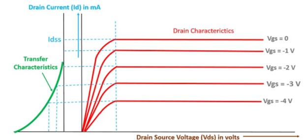
Output Characteristics or Drain Characteristics
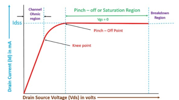
- In the absence of external bias: In this case, as there is no voltage between gate and source terminal, thus, the drain current will flow from drain terminal to source terminal. We have already discussed in the working of JFET that majority charge carriers flow from source to drain and as a consequence of which the current flows from drain to source.
|
Fig 4 Output characteristics in absence of external source
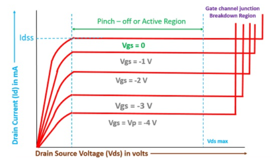
- With external bias: When the external bias is applied to the gate-source terminal, the gate-source terminal becomes reversed bias externally. Obviously, if we are supplying an external voltage, then we can achieve the pinch-off point quite early as compared to the circuit which is not biased.
|
Fig 5 Output characteristics with external source
The transfer characteristics can be determined by observing different values of drain current with variation in gate-source voltage provided that the drain-source voltage should be constant. The transfer characteristics are just opposite to drain characteristics.
|
Fig 6 Transfer characteristics of N-channel JFET
Key takeaway
- An FET is a three-terminal amplifying device.
- Its terminals are source, gate, and drain, which acts respectively like emitter, base, and collector of a normal transistor.
Operating point
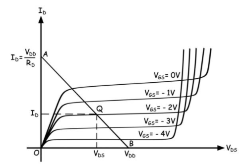
The output characteristics of N-channel JFET with external biased was discussed in above section. For getting the operating point we just connect the maximum value of VDS and ID in the characteristics by a straight line. This is called as dc load line. When this line is formed only the dc components are considered as shown in figure below.
|
Fig 7 Load – Line Characteristics
Biasing
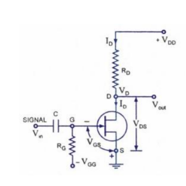
For Fixed Biased the value of VGS should be such that ID is obtained. In case if JFET the value of ID is limited by the saturation current IDS. Due to high input impedance, there is no gate current flowing and the dc voltage of gate is set by the voltage divider.
|
Fig 8 Fixed Biased FET
The dc bias is obtained by using battery which keeps the gate negative with respect to the source and no current flows through RG. The value of IG = 0. The battery provides voltage VGS to bias N-channel JFET and there is no current from battery VGG. If any ac signal is developed across RG, the dc voltage drop across RG = 0.
The value of VGS will be
VGS = -VG-VS = -VGG-0 = -VGG
The current ID causes voltage drop across RD
VRD = ID RD
Vout = VDD-IDRD
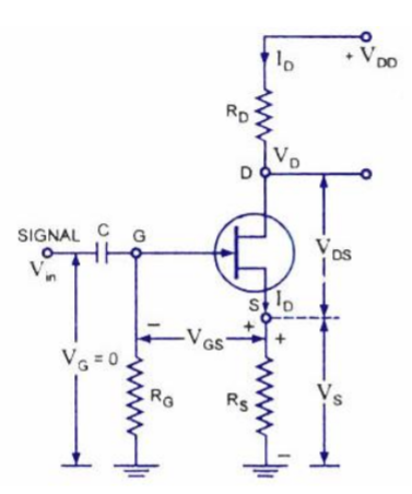
For Self-Biased the figure is shown below. It is the most common method of biasing used. The N-channel JFET is as there is no gate current through reverse biased gate source the gate current IG=0 and VG = IGRG=0. The value of voltage at source will be VS = IDRS
|
Fig 9 Self Biased FET
The equation for VGS is given as
VGS = VG-VS =0-IDRS = -IDRL
The self-biasing of a JFET stabilizes its Q-point against any change in its parameters like transconductance.
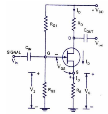
The Potential Divider Bias for JFET is shown below. The resistors RG1 and RG2 form potential divider across VDD. The voltage V2 across RG2 provides necessary bias. The gate is reverse bias and IG=0.
VG = V2= (VDD/RG1*RG2) *RG2
|
Fig 10 Potential Divider Bias Circuit
The operating point will be
ID = (V2-VGS)/RS
VDS = VDD-ID(RD+RS)
Key takeaway
For fixed bias Vout = VDD-IDRD
For Self-Biased the gate current IG=0 and VG = IGRG=0
For Potential Divider Biased
The operating point will be
ID = (V2-VGS)/RS
VDS = VDD-ID(RD+RS)
As we know FET provide high input impedance and is an excellent amplifier with voltage gain. The small signal low frequency model is shown below for n-channel JFET. From below figure we can understand that the input impedance is represented by open circuit and hence IG= 0. The resistance rd represents the output impedance.
The gate to source voltage only controls the drain to source current for JEFT. The transconductance factor gm is
 Id = gm
 VGS
VGS
The equation for output impedance rd is
rd =  |for VGS constant
MOSFETs are three terminal devices with a Gate, Drain and Source and both P-channel (PMOS) and N-channel (NMOS) MOSFETs are available. The main difference this time is that MOSFETs are available in two basic forms:
- Depletion Type – the transistor requires the Gate-Source voltage, ( VGS ) to switch the device “OFF”. The depletion mode MOSFET is equivalent to a “Normally Closed” switch.
- Enhancement Type – the transistor requires a Gate-Source voltage, ( VGS ) to switch the device “ON”. The enhancement mode MOSFET is equivalent to a “Normally Open” switch.
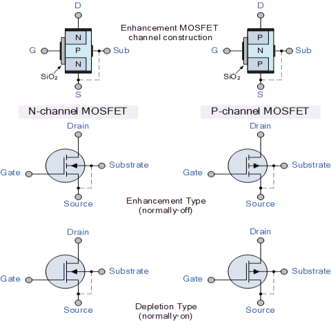
The symbols and basic construction for both configurations of MOSFETs are shown below.
|
Fig 11 Symbols of MOSFET
The four MOSFET symbols above show an additional terminal called the substrate and is not normally used as either an input or an output connection but instead it is used for grounding the substrate. It connects to the main semiconductive channel through a diode junction to the body or metal tab of the MOSFET.
The line in the MOSFET symbol between the drain (D) and source (S) connections represents the transistors semiconductive channel. If this channel line is a solid unbroken line then it represents a “Depletion” (normally-ON) type MOSFET as drain current can flow with zero gate biasing potential.
If the channel line is shown as a dotted or broken line, then it represents an “Enhancement” (normally-OFF) type MOSFET as zero drain current flows with zero gate potential. The direction of the arrow pointing to this channel line indicates whether the conductive channel is a P-type or an N-type semiconductor device.
|
Fig 12 N-channel MOSFET
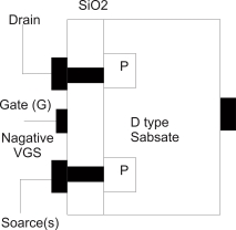
The construction of the Metal Oxide Semiconductor FET is different to that of the Junction FET.
Both the Depletion and Enhancement type MOSFETs use an electrical field produced by a gate voltage to alter the flow of charge carriers, electrons for n-channel or holes for P-channel, through the semi-conductive drain-source channel.
The gate electrode is placed on top of a very thin insulating layer and there are a pair of small n-type regions just under the drain and source electrodes.
With the insulated gate MOSFET device no such limitations apply so it is possible to bias the gate of a MOSFET in either polarity, positive (+ve) or negative (-ve).
This makes the MOSFET device especially valuable as electronic switches or to make logic gates because with no bias they are normally non-conducting and this high gate input resistance means that very little or no control current is needed as MOSFETs are voltage-controlled devices.
Both the p-channel and the n-channel MOSFETs are available in two basic forms, the Enhancement type and the Depletion type.
MOSFET Construction, Operation and Characteristics
MOSFET is another type of field effect transistor. The MOSFET has become one of the most important devices used in design and construction computers
MOSFET [metal oxide semiconductor field effect transistor]
Type of MOSFET
- Depletion type MOSFET
- Enhancement type MOSFET
- Power MOSFET
Enhancement type MOSFET: classified in to two type n. channel or p. channel E MOSFET
- N-channel E MOSFET
- P-channel E MOSFET
N-channel E MOSFET
|
Fig 13 N-Channel MOSFET
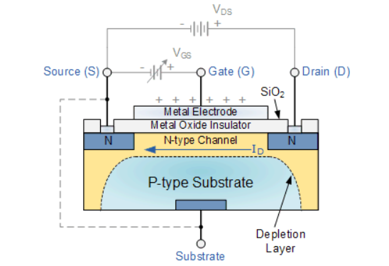
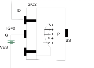
- A slab of P-type semiconductor is used as substrate. The substrate is sometimes connected to the source otherwise it is brought out as the fourth terminal.
- The drain and source terminal are connected to the n-type doped regions through the metallic contacts.
- The insulating sio2 layer is still present which isolates gate terminal from the substrate.
Effect of the insulting sio2 layer:
Due to the presence of the sio2 layer between gate terminal and n-type channel the i/p impedance of MOSFET is very high this is a desirable fracture of a MOSFET. Due to high i/p impedance the gate current IG= 0 for the d.c operating conditions.
Operation: the operation can be explained with two different operating
- Operation with VGS = 0
- Operation when VGS is +ve
Operating with VGS = 0 Volt
If VGS = 0 and a positive voltage is applied between its drain and source then due to the absence of the n-type channel a zero drain current will result.
Operation when Vgs Positive:
The positive potential at the gate terminal will repel the holes present in the p-type substrate.
|
Fig 13 Formation of induced channel in n-channel enhancement MOSFET
This creates a depletion region near the sio2 insulating layer. But the minority carriers i.e., the electrons in the p-type substrate will be attracted towards the gate terminal and gather near the surface of sio2 as shown above
As we increase the positive VGS the number of e- gathering near the sio2 layer increases to such an extent that it creates an induced n-channel which connects the n-type doped regions.
The drain current then starts flowing through this induced channel. The value of VGS at which this conduction begins is called as the threshold Voltage & is indicated
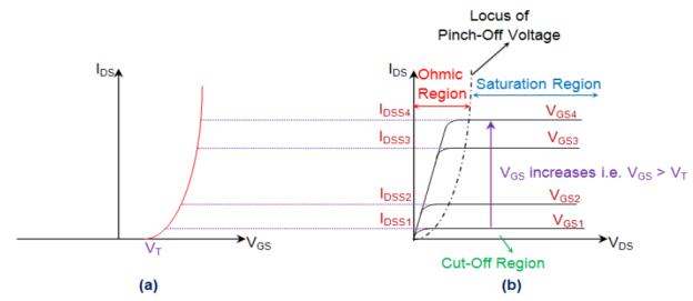
MOSFET is seen to exhibit three operating regions viz.,
- Cut-Off Region
Cut-off region is a region in which the MOSFET will be OFF as there will be no current flow through it. In this region, MOSFET behaves like an open switch and is thus used when they are required to function as electronic switches.
- Ohmic or Linear Region
Ohmic or linear region is a region where in the current IDS increases with an increase in the value of VDS. When MOSFETs are made to operate in this region, they can be used as amplifiers.
- Saturation Region
In saturation region, the MOSFETs have their IDS constant inspite of an increase in VDS and occurs once VDS exceeds the value of pinch-off voltage VP. Under this condition, the device will act like a closed switch through which a saturated value of IDS flows. As a result, this operating region is chosen whenever MOSFETs are required to perform switching operations.
|
Fig 14: (a) Transfer Characteristics (b) Output Characteristics of NMOs
Key takeaway
Due to the presence of the sio2 layer between gate terminal and n-type channel the i/p impedance of MOSFET is very high this is a desirable fracture of a MOSFET. Due to high i/p impedance the gate current IG= 0 for the d.c operating conditions.
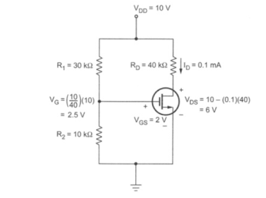
For the circuit shown in figure assume that R1 = 30KΩ and R2 = 10 KΩ. Rd = 40KΩ . Vdd = 10V and VT=1V , Vgs = 2V and K = 0.1mA /V2 . Find Id and VDS
|
VG = VGS = (R2/R1+R2) VDD = (10/10+30) (10) = 2.5V
Assuming that the MOSFET is biased in the saturation region the drain current is
VDS = VDD – ID RD = 10 – (0.1)(40) = 6V.
|
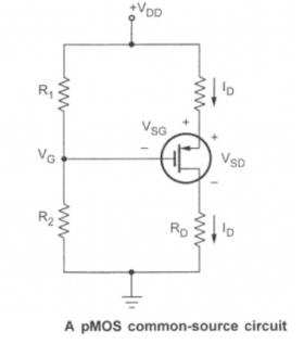
Here, the source is tied to +VDD, Which, become signal ground in the a.c. equivalent circuit. Thus, it is also a common-source circuit.
The d.c. analysis for this circuit is essentially the same as for the n-channel MOSFET circuit. The gate voltage is given by,
VG = (R2/R1 + R2) (VDD)
And the source to gate voltage is given by
VSG = VDD -VG
Assuming VGS <VT or VSG > |VT| the device in the saturation region and the drain current is given by
ID = K(VSG + VT) 2
And the source to drain voltage is given by
VSD = VDD – ID RD
If VSD > VSD (sat) then MOSFET is in saturation region.
IF VSD < VSD(sat) MOSFET is in non-saturation region.
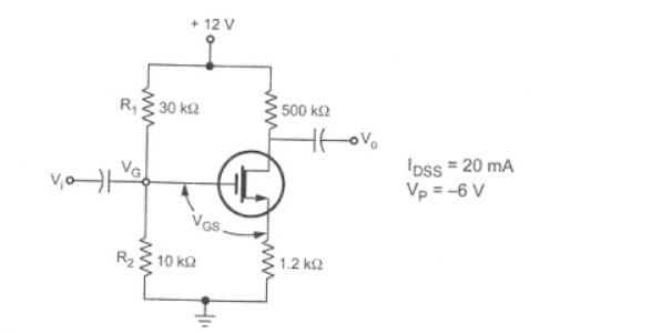
Q) For the circuit shown in figure calculate ID , VDS, VG and VS
|
Applying KVL to the input circuit.
VGS = VG – VS
= 3 – IS RS Since VS = IS RS
= 3 – ID RS Since ID = IS
We have
ID = IDSS ( 1 – VGS / VP ) 2
Substituting the value of VGS we get
ID = IDSS ( 1 – (3 – ID RS)/Vp) 2 = 20 x 10 -3 ( 1 – ( 3 – ID x 1.2 x 10 3 / -6)
= 20 x 10 -3 ( 1 – [ (-0.5) + 200 ID ]) 2 = 20 x 10 -3 ( 1.5 -2)
= 20 x 10 -3 (2.25 – 600ID + 40000ID 2)
I D = 0.045 – 12 I D + 800 I D 2
800 I D 2 – 13 I D + 0.045 =0
Solving for quadratic equation we get
= -(-13) ± [ (13) 2 – 4(800)(0.045)] ½ / 2(800)
= 13 ± [ 169 -144] ½ / 1600 = 13 ±  / 1600 = 13 ± 5 /1600 = 5mA or 11.25 mA
If we calculate the value of VDS taking ID = 11.25mA we get
VDS = VDD – ID ( RD + RS)
= 12 – 11.25 x 10 -3 ( 500 + 1.2 x 10 3)
= 12 – 19.125 = -7.125
Practically the value of VDS must be positive hence ID= 11.25 mA is invalid
Hence take ID = 5mA
VDS = VDD – ID (RD + RS) = 12 – 5 x 10 -3 (500 + 1.2 x 10 3) = 12 – 8.5 = 3.5 V
VGS = 3 – ID RS = 3- 5 x 10 -3 x 1.2 x 10 3 = 3 – 6 = -3 V
Vs = ID RS = 5 x 10 -3 x 1.2 x 10 3 = 6V
Common Source Amplifier
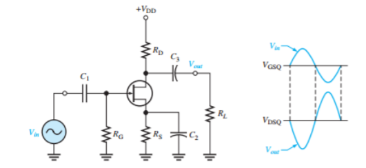
In CS amplifier the ac input is applied to gate and the output is taken across drain. This configuration has a bypass source resistor which connects the source to the ground. The below figure is shown of a self-biased common source n-channel JFET amplifier which is capacitively coupled. The resistor RG keeps gate at 0V and prevents loading of ac signal source.
The capacitor C2 keeps the source of JFET at ac ground. The gate source voltage swing between VGSQ above and below its Q-point and causing swig in drain current too. The voltage drop across RD increases as the drain current increases. The VDS is 1800 out of phase with VGS.
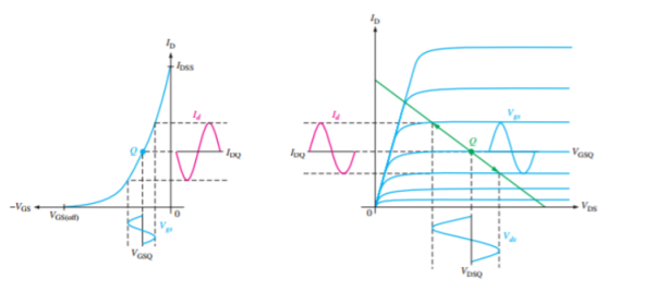
The figure below shows sinusoidal variation VGS produces corresponding sinusoidal variation in ID. The value of VGS swings to more negative value of Q-point ID decreases from its Q-point. The value of ID increases when VGS swings to a less negative value. The signal at the gate drives the drain current above and below the Q-point on the load line.
|
Fig 15 Self-Biased CS amplifier
Lines projected from the peaks of the gate voltage across to the ID axis and down to the VDS axis indicate the peak-to-peak variations of the drain current and drain-to-source voltage, as shown. Because the transfer characteristic curve is nonlinear, the output will have some distortion. This can be minimized if the signal swings over a limited portion of the load line.
|
Fig 16 Transfer characteristics for CS amplifier
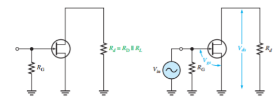
The ac equivalent circuit is shown below. The input resistance to JFET is very high so all of the input voltage from the signal source appears at the gate with small drop across internal source resistance.
|
Fig 17 AC equivalent Circuit
Vgs = Vin
The voltage gain will be Av = gmRd
The input which is actually seen by signal source is RG in parallel with FET input resistance VGS IGSS.
Rin = RG||(VGS/IGSS)
Common Drain Amplifier
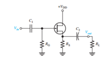
A common-drain JFET amplifier is one in which the input signal is applied to the gate and the output is taken from the source, making the drain common to both. Because it is common, there is no need for a drain resistor. A common-drain JFET amplifier is shown in Figure below. A common-drain amplifier is also called a source-follower. Self-biasing is used in this particular circuit. The input signal is applied to the gate through a coupling capacitor, C1, and the output signal is coupled to the load resistor through C2
|
Fig 18 Self Biased CD amplifier
The expression for voltage gain will be
AV = 
AV = 
The gain is always<1. The RG is in parallel with RIN at gate so, the total input resistance is
Rin = RG||RIN (gate)
Common Gate Amplifier
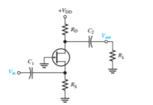
A self-biased common-gate amplifier is shown in figure. The gate is connected directly to ground. The input signal is applied at the source terminal through C1. The output is coupled through C2 from the drain terminal.
|
Fig 19 Common gate amplifier
The voltage gain is given by
Av =  =
=  =
=  = AV =
Rd = RD||RL
The input current is given by
Vin = Vgs
The input resistance at the source terminal is
Rin=  =
= 
Rin = 1/gm
Key takeaway
For Common source amplifier
Vgs = Vin
The voltage gain will be Av = gmRd
For Common gate amplifier
Rin = 1/gm
For common drain amplifier
AV = 
The gain is always<1
Reference:
1 “Electronic Devices and Circuit Theory”, Boylestad and Nashelsky, PEARSON
PUBLICATION.
2 “Electronic devices and circuits”, Salivahanan, Suresh Kumar, Vallavaraj,
TMH, 1999
3 “Integrated Electronics, Analog and Digital Circuits and Systems”, J. Millman
and Halkias, TMH, 2000
4 “Micro Electronic Circuits”, Sedra and Smith, Oxford University Press, 2000
5 “Electronic Devices and Circuits”, David A Bell, Oxford University Press, 2000
