UNIT-1
BASICS OF SEMICONDUCTOR PHYSICS
SEMICONDUCTOR CARRIER MODELLING
Semiconductors are materials that have conductivity between conductors and insulators.
Semiconductors can be pure elements, such as silicon or germanium, or compounds such as gallium arsenide or cadmium selenide.
They are not good conductors nor good insulators as their name “semi”-conductors.
These materials such as silicon (Si), germanium (Ge), and gallium arsenide (GaAs), have electrical properties somewhere in the middle, between those of a “conductor” and an “insulator”.
They have very few “free electrons” because their atoms are closely grouped in a crystalline pattern called a “crystal lattice” but electrons are still able to flow, but only under special conditions.
Carriers are the entities that transport charge from place to place inside a material and hence give rise to electrical currents. In everyday life the most commonly encountered type of carrier is the electron, the subatomic particle responsible for charge transport in metallic wires Within semiconductors one again encounters the familiar electron, but there is also a second equally important type of carrier—the hole. We will study the semiconductor carrier modelling to get a good knowledge of semiconductor.
1.1.1 Bonding Model
The isolated Si atom was found to contain four valence electrons. A Si atom is not interacting with other atoms; Si atoms exhibit a bonding that involves an attraction between each atom and its four nearest neighbours.
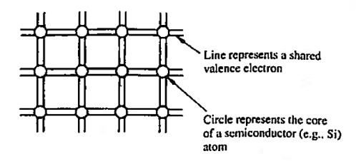
The implication here is that in going from isolated atoms to the collective crystalline state, Si atoms come to share one of their valence electrons with each of the four nearest neighbours. This covalent bonding, or equal sharing of valence electrons with nearest neighbours, and the mere fact that atoms in the diamond lattice have four nearest neighbours, give rise to the idealized semiconductor representation, the bonding model, shown in Figure 1. This is giving two dimensional representation of the model.
|
Figure 1: Bonding Model
Each circle in the bonding model represents the core of a semi-conductor atom, while each line represents a shared valence electron.
There are eight lines connected to each atom because any given atom not only contributes four shared electrons but must also accept four shared electrons from adjacent atoms.
|
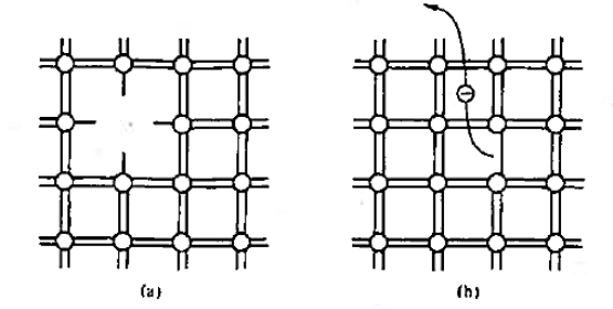
Figure 2: Bonding Model (a) Visualisation of misting atom or point defect (b) Breaking of an atom.to-atom bond and freeing of an electron.
With the help of bonding model we can visualise the following factor as shown in figure 2. The bonding model is used to picture a point defect, a missing atom, in the lattice structure. It helps to visualise the breaking of an atom-to-atom bond and the associated release or freeing of an electron.
We know that Bond breaking occurs at high temperature (at T> 0 K) and defects occur naturally in all semiconductors.
The basic model shown in figure 1 is strictly valid for an entire semiconductor only at T = 0 K when the semiconductor contains no defects and no impurity atoms.
If we want to describe the spatial aspect of semiconductor only bonding model is not sufficient, we need to know about the energy aspects too. So we will now see the energy band model.
1.1.2 Energy Band Model
Let us begin the conceptual path leading to the energy band model by recalling the situation inside an isolated Si atom. Ten of the 14 electrons inside an isolated Si atom are tightly bound to the nucleus and are unlikely to be significantly perturbed by normal atom—atom interactions. The remaining four electrons are rather weakly bound and, if unperturbed, occupy four of the eight allowed energy states immediately above the last core level. Moreover, it is implicitly understood that the electronic energy states within a group of Si atoms, say N Si atoms, are all identical -as long as the atoms are isolated, that is, far enough apart so that they are non-interacting.
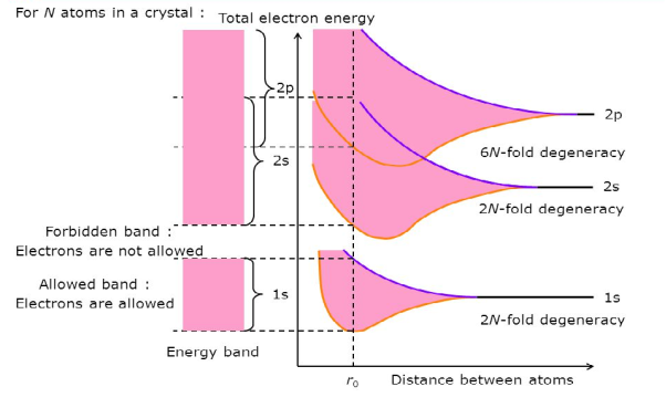
If N atoms are brought into close proximity it is quite reasonable to expect a modification in the energy states of the valence electrons. Starting with N-isolated Si atoms, and conceptually bringing the atoms closer and closer together, one finds the interatomic forces lead to a progressive spread in the allowed energies. The spread in energies gives rise to closely spaced sets of allowed-states is known as energy bands.
Consider an isolated silicon atom; its energy levels are quantized. When two identical atoms are brought closer together, the quantized energy levels hybridize and split into two different levels because of the mutual interaction of the two atoms. More generally, when N atoms are moved closer until they reach the equilibrium inter-atomic distance d, the energy levels split into N levels. These N levels are very close to each other if N is large (which is the case in a crystal) so that they eventually form a continuous energy band.
|
Figure 3: Formation of Energy band as a function of interatomic distance (distance between atoms)
Bands are formed by the closely spaced orbitals.
There are three types of bands:
1. Valance Bands: A valence band is a group of orbitals that contain electrons in the shell. Or we can say It is also defined as the energy band that comprises of valence electrons present in the outermost shell of an atomic structure.
These valence electrons, when provided with sufficient energy, get changed into free electrons and moves to the conduction band thereby causing conductivity. It is at a lower energy level than the conduction band in the energy level diagram.
2. Conduction Band: A conduction band is a group of empty orbitals of the shells that do not contain any electron due to their configuration making the orbitals of higher energy levels.
When the electrons pass from the valance band to the conduction band these solids conduct electricity with the flow of charges in the form of electrons.
3. Forbidden Energy Band: These two bands are separated by a certain amount of energy known as the forbidden energy gap. In this band not a single electron is available. Its diagram is named Band Gap.
Key Takeaways
- Semiconductors are materials that have conductivity between conductors and insulators.
- Bonding Model gives the knowledge of bonding between the atoms. The bonding model is used to picture a point defect, a missing atom, in the lattice structure. It helps to visualise the breaking of an atom-to-atom bond and the associated release or freeing of an electron.
- Energy Bond Model gives the energy aspect of atoms to get good knowledge of semiconductor.
- The spread in energies gives rise to closely spaced sets of allowed-states is known as energy bands.
- Bands are formed by the closely spaced orbitals.
- There are three types of bands: Valence band, conduction band, Forbidden Energy Band
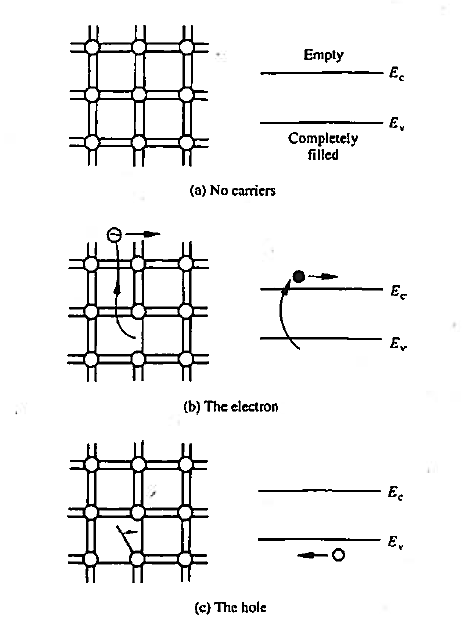
We already know that that there are no carriers or possible current flow if the bonding model has no broken bonds. Equivalently, in the energy band model, if the valence band is completely filled with electrons and the conduction band is devoid of electrons. There are no carriers or possible current flow. This lack of carriers and associated current flow is easy to understand in terms of the bonding model where the shared electrons are viewed as being tied to the atomic cores.
As accurately portrayed in the energy band model, however, the valence band electrons actually move about in the crystal. How is it then that no current can arise from this group of electrons? As it turns out, the momentum of the electrons is quantized in addition to their energy. Moreover, for each and every possible momentum state in a band, there is another state with an oppositely directed momentum of equal magnitude. Thus, if a band is completely filled with electrons, the net momentum of the electrons in the band is always identically zero. It follows that no current can arise from the electrons in a completely filled energy band.
|
Figure 4: Visualization of carriers using the bonding model (left) and the energy band model (left) (a) No-carrier situation (b) Visualization of electrons (c) Visualization of hole.
The electrons that do give rise to charge transport are visualized in Figure above. When a Si—Si bond is broken and the associated electron is free to wander about the lattice, the released electron is a carrier. Equivalently, in terms of the energy band model, excitation of valence band electrons into the conduction band creates carriers; that is, electrons in the conduction band are carriers.
Note that the energy required to break a bond in the bonding model and the band gap energy are one and the same thing. Likewise, free bonding-model electrons and conduction band electrons are just different names for the same electrons.
In addition to releasing an electron the breaking of a Si-Si bond also creates a missing bond or void in the bonding structure.
By bonding modelled one can visualize the movement of this missing bond from place to place in the lattice as a result of nearby bound electrons jumping into the void
By the energy band model one can visualize the removal of an electron from the valence band creates an empty state in vast sea of filled stales. the empty slate in the valence band is the second type of carnet found in semi-conductors—the hole. Both electrons and holes participate in the operation of most semiconductor devices.
Key Takeaways
- When a Si—Si bond is broken and the associated electron is free to wander about the lattice, the released electron is a carrier.
- Note that the energy required to break a bond in the bonding model and the band gap energy are one and the same thing.
- The empty slate in the valence band. is the second type of carnet found in semi-conductors—the hole.
- Both electrons and holes participate in the operation of most semiconductor devices.
The Valence band and conduction band are separated by a certain amount of energy known as the forbidden energy gap. In this band not a single electron is available. Its diagram is named Band Gap.
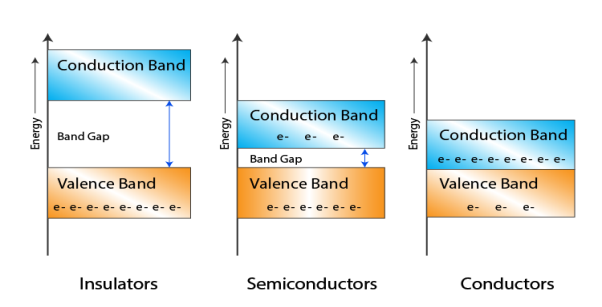
The major difference between materials lies not in the nature of the energy bands, but rather in the magnitude of the energy gap. Insulators are those having wide band gap.
The thermal energy available at room temperature excites very few electrons from the valence band into the conduction band; thus very few carriers exist inside the material
Metals: very small or no band gap exists at all due to an overlap of the valence and conduction bands. An abundance of carriers leads to excellent conductors. Whereas Semiconductors is an intermediate case
At 300K, EG=1.42 eV in GaAs, EG=1.12 eV in Si, EG=0.66 eV in Ge.Thermal energy, by exciting electrons from the valence band into the conduction band, creates a moderate number of carriers
Let us distinguish between conductors, semiconductors, and insulators based on these bands.
|
Figure 5: Conductors, Semiconductors, and Insulators based on these bands.
- In Conductors: The valance band and the conduction band overlap each other. This makes it easy for electricity to pass through them. In conductors, the valence band is either not fully occupied with electrons, or the filled valence band overlaps with the empty conduction band. In general, both states occur at the same time, the electrons can therefore move inside the partially filled valence band or inside the two overlapping bands. In conductors, there is no bandgap between the valence band and conduction band.
- In Semi-conductors: there is a slight gap between the conduction band and the valance band. This bandgap is less than or equal to 1.4 eV. The electrons from the valance shell take a little energy to excite from the valance band to the conduction band. Even in semiconductors, there is a bandgap, but compared to insulators it is so small that even at room temperature electrons from the valence band can be lifted into the conduction band. The electrons can move freely and act as charge carriers.
- In Insulators: In insulators, the valence band is fully occupied with electrons due to the covalent bonds. To achieve conductivity, electrons from the valence band have to move into the conduction band. the energy gap is considerably large and the electrons of the valance band cannot be excited to the conduction band before the melting or the dissociation of the solid. This means that under the practically ambient condition it cannot conduct electricity.
Key Takeaways
- The Valence band and conduction band are separated by a certain amount of energy known as the forbidden energy gap.
- Insulators are those having wide band gap.
- Metals: very small or no band gap exists at all due to an overlap of the valence and conduction bands
- Semiconductors is an intermediate case
- On the basis of band theory, we can classify the materials as conductors, semiconductors, and insulators based on these bands.
We will try to understand some important point related to the carriers i.e. electrons and holes in the Semiconductor.
1.4.1 EFFECTIVE MASS
Mass of the carrier is one of the basic but important property. However, the carrier mass is not a simple property and cannot be easily defined by quoting a number.
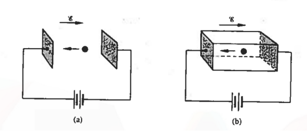
We however already know the fact that effective mass not simple mass. "Effective" mass of electrons within a crystal is a function of the semiconductor material (Si, Ge, etc.) and is different from the mass of electrons within a vacuum.
|
Figure 6: An electron moving in response to an applied electric field (a) within a vacuum, and (b) within a semiconductor crystal
Let us first consider the motion of electrons in a vacuum. An electron of rest mass m0 is moving in a vacuum between two parallel plates under the influence of an electric field , then, according to Newton's second law, the force F on the electron will be
 ……….. (1)
where v is the electron velocity and t is time.
Next consider electrons (conduction band electrons) moving between the two parallel end faces of a semiconductor crystal under the influence of an applied electric field, as envisioned in Figure 6(b).
Electrons moving inside a semiconductor crystal will collide with semiconductor atoms, thereby causing a periodic deceleration of the carriers. However, not Eq. (1) should not apply to the portion of the electronic motion occurring between collisions. Under the effect of applied electric field, electrons in a crystal are also subject to complex crystalline fields.
Thus the motion of carriers in a crystal can be described only by using Quantum Mechanics, the formalism appropriate for atomic-sized systems. Fortunately, if the dimensions of the crystal are large compared to atomic dimensions, the complex quantum mechanical formulation for the carrier motion between collisions simplifies to yield an equation of motion given below
 ………… (2)
Where m*n is the electron effective mass.
A similar equation can be written for holes with —q q and m*n
  m*p.
m*p.
This is a very significant result. It allows us to conceive of electrons and holes as quasi-classical particles and to employ classical particle relationships in most device analyses.
Although the effective mass formulation is a significant simplification, it should be mentioned that the carrier acceleration can vary with the direction of travel in a crystal; i.e. The effective masses can have multiple components. Moreover, depending on how a macroscopic observable is related to the carrier motion, a different grouping of mass components can lead to a different m* being utilized in a particular relationship.
There are, for example, cyclotron resonance effective masses, conductivity effective masses, density of states effective masses, among others. It is also probably not too surprising that the effective masses vary somewhat with temperature.
1.4.2 INTRINSIC CARRIER CONCENTRATION
Carrier Numbers in Intrinsic Material
The term intrinsic semiconductor in common usage refers to an extremely pure semiconductor sample containing an insignificant amount of impurity atoms. More precisely, an intrinsic semiconductor is a semiconductor whose properties are native to the material (that is, not caused by external additives). The number of carriers in an intrinsic semiconductor "fits into the scheme of things in that it is an identifiable intrinsic property of the material.
Defining, quite generally,
n = number of electrons/cm3
p - number of holes/cm3
existing inside a semiconductor, then, given an intrinsic semiconductor under equilibrium conditions, one finds
n =p= ni, ………..(1)
|
The electron and hole concentrations in an intrinsic semiconductor are equal because carriers within a very pure material can be created only in pairs.
If a semiconductor bond is broken, a free electron and a missing bond or hole are created simultaneously. Likewise, the excitation of an electron from the valence band into the conduction band automatically creates a valence band hole along with the conduction band electron.
Also note that the intrinsic carrier concentration, although large in an absolute sense, is relatively small compared with the number of bonds that could be broken.
For example, in Si there are 5 x 10²² atoms/cm3 and four bonds per atom, making a grand total of 2 x 10²³ bonds or valence band electrons per cm3. Since ni =1010/cm3, one finds less than one bond in 1013 broken in Si at room temperature.
1.4.3 DOPING
The process by which an impurity is added to a semiconductor is known as Doping. The amount and type of impurity which is to be added to a material has to be closely controlled during the preparation of extrinsic semiconductor. Generally, one impurity atom is added to a 108 atoms of a semiconductor.
Doping is basically manipulation of Carrier Numbers.
Doping is the addition of controlled amounts of specific impurity atoms with the express purpose of increasing either the electron or the hole concentration.
To increase the electron concentration, one can add either phosphorus, arsenic, or antimony atoms to the Si crystal, with phosphorus followed closely by arsenic being the most commonly employed donor (electron-increasing) dopants.
To increase the hole concentration, one adds either boron, gallium, indium, or aluminium atoms to the Si crystal, with boron being the most commonly employed acceptor (hole-increasing) dopant.
To understand how the addition of impurity atoms can lead to a manipulation of carrier numbers, it is important to note donors are all from Column V in the Periodic Table of Elements, while all of the acceptors are from Column III in the Periodic Table of Elements.
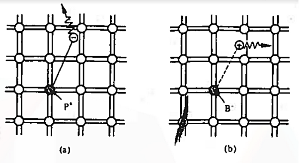
When a Column V element with five valence electrons is substituted for a Si atom in the semiconductor lattice, four of the five valence electrons fit snugly into the bonding structure. The fifth donor electron, however, does not fit into the bonding structure and is weakly bound to the donor site. At room temperature this electron is readily freed to wander about a lattice and hence becomes a carrier. Please note that this donation (hence the name "do-nor") of carrier electrons does not increase the hole concentration. The donor ion left behind when the fifth electron is released cannot move, and there is no broken atom—atom bonds associated with the release of the fifth electron.
The Column III acceptors have three valence electrons and cannot complete one of the semiconductor bonds when substituted for Si atoms in the semiconductor lattice. The Column III atom, however, readily accepts (hence the name "acceptor") an electron from a nearby Si—Si bond, thereby completing its own bonding scheme and in the process creating a hole that can wander about the lattice. Here again there is an increase in only one type of carrier. The negatively charged acceptor ion (acceptor atom plus accepted electron) cannot move, and no electrons are released in the hole-creation process.
|
Figure 7: Visualization of (a) donor and (b) acceptor action using the bonding model.
The dopant action is reasonably understandable with the help of bonding-model. We noted that the fifth donor electron was rather weakly bound and readily freed at room temperature. Here the term "weakly bound" simply means that it takes =1 eV to break Si—Si bonds and very few of the Si—Si bonds are broken at room temperature.
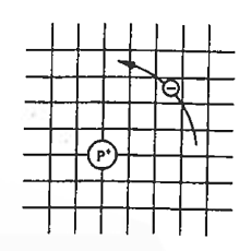
Now try to figure it out with te help of energy band. Let us concentrate first on the binding energy of the fifth donor electron. Crudely speaking, the positively charged donor-core-plus-fifth-electron may be likened to a hydrogen atom. Conceptually, the donor core replaces the hydrogen-atom nucleus and the fifth donor electron replaces the hydrogen-atom electron.
In the real hydrogen atom, the electron moves of course in a vacuum, can be characterized by the mass of a free electron and has a ground-state binding energy of — 13.6 eV.
In the pseudo-hydrogen atom, on the other hand, the orbiting electron moves through a sea of Si atoms and is characterized by an effective mass. Hence, in the donor or pseudo-atom case, the permittivity of free space must be replaced by the permittivity of Si and m0 must be replaced by m*n. We therefore conclude that the binding energy (EB) of the fifth donor electron is approximately
|
where Ks is the Si dielectric constant (Ks = 11.8).
|
Figure 8: Pseudo hydrogen atom model for the donor-site bond.
When an electron is released from a donor it becomes a conduction band electron. If the energy absorbed at the donor is precisely equal to the electron binding energy, the released electron will moreover have the lowest possible energy in the conducting band—namely, EC. Adding energy  to the bound electron, in other words, raises the electron's energy to EC.
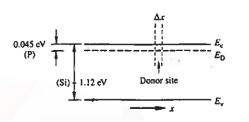
Hence, we are led to conclude that the bound electron occupies an allowed electronic level an energy  below the conduction band edge, or, as visualized in figure 9 donor sites can be incorporated into the energy band scheme by adding allowed electronic levels at an energy ED = EC -
  .
.
Note that the donor energy level is represented by a set of dashes instead of a continuous line, because an electron bound to a donor site is localized in space; i.e., a bound electron does not leave the general  vicinity of the donor. The relative closeness of ED to EC of course reflects the fact that EC - ED =
  .
.
|
Figure 9: Addition of the E =ED donor slevels in the energy band diagram. Dashes of width  emphasize the localized nature of the bound donor-sites states.
|
Figure 10: Visualization of (a) donor and (b) acceptor action using the energy baud model.
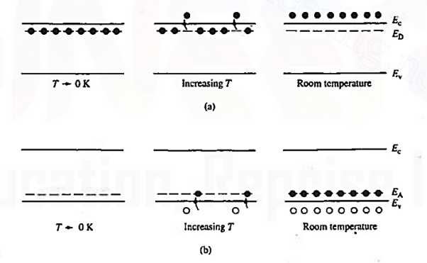
The actual visualization of dopant action using the energy band model is pictured in figure 10. Examining the left-hand side of Figure 10 (a), one finds all the donor sites filled with bound electrons at temperatures T 0K. This is true because very little thermal energy is available to excite electrons from the donor sites into the conduction band at these very low temperatures.
As the temperature is increased, the situation changes with more and more of the weakly bound electrons being donated to the conduction band. At room temperature the ionization of the donors is all but total, giving rise to the situation pictured at the extreme right of Figure 10(a).
The situation for acceptors is completely analogous. As visualized in Figure 10(b), acceptors introduce allowed electronic levels into the forbidden gap at an energy slightly above the valence band edge. At low temperatures, all of these sites will be empty—there is insuffient energy at temperatures T 0 K for a valence band electron to make the transition to an acceptor site.
Increasing temperature, implying an increased store of thermal energy, facilitates electrons jumping from the valence band onto the acceptor levels. The removal of electrons from the valence band of course creates holes. At room temperature, essentially all of the acceptor sites are filled with an excess electron and an increased hole concentration is affected in the material.
An impurity that can act as either a donor or an acceptor is referred to as an amphoteric dopant.
The purpose of adding impurity in the semiconductor crystal is to increase the number of free electrons or holes to make it conductive.
If a Pentavalent impurity, having five valence electrons is added to a pure semiconductor a large number of free electrons will exist. Which make a n-type extrinsic semiconductor?
If a trivalent impurity having three valence electrons is added, a large number of holes will exist in the semiconductor. Which make a p-type extrinsic semiconductor?
Key Takeaway
- "Effective" mass of electrons within a crystal is a function of the semiconductor material (Si, Ge, etc.) and is different from the mass of electrons within a vacuum.
- The complex quantum mechanical formulation for the carrier motion between collisions simplifies to yield an equation of motion given below
 Where m*n is the electron effective mass.
- It is also probably not too surprising that the effective masses vary somewhat with temperature.
- An intrinsic semiconductor under equilibrium conditions follows n =p= ni,
- The electron and hole concentrations in an intrinsic semiconductor are equal because carriers within a very pure material can be created only in pairs.
- The process by which an impurity is added to a semiconductor is known as Doping. Doping is basically manipulation of Carrier Numbers.
- If a Pentavalent impurity, having five valence electrons is added to a pure semiconductor a large number of free electrons will exist. Which make a n-type extrinsic semiconductor?
- If a trivalent impurity having three valence electrons is added, a large number of holes will exist in the semiconductor. Which make a p-type extrinsic semiconductor?
The energy band model indicated that the total number of allowed states in each band was four times the number of atoms in the crystal. But we don’t have idea about how the allowed states were distributed in energy; i.e., how many states were to be found at any given energy in the conduction and valence bands.
We are now interested in the energy distribution of states or density of states because the state distribution is an essential component in determining carrier distributions and concentrations.
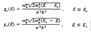
The formula of the desired density of states is calculated using quantum-mechanical considerations. It is given by
|
where gc(E) and gv(E) are the density of states at an energy E in the conduction and valence bands, respectively.
The density of states can be likened to the description of the seating in a football stadium, with the number of seats in the stadium a given distance from the playing field corresponding to the number of states specified energy interval froth Ec or Ev.
|
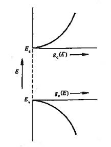
Figure 11: General energy dependence of gc(E) and gv(E) near band edges
gc(E) is zero at Ec and increases as the square root of energy when one proceeds upward into the conduction band.
Similarly, gv(E) is precisely zero at Ev, and increases with the square root of energy as one proceeds downward from Ev, into the valence band.
Also note that differences between gc(E) and gv(E) stem from differences in the carrier effective masses. If m*n were equal to m*p, the seating (states) on both sides of the football field (the band gap) would be mirror images of each other. Finally, considering closely spaced energies E and E+ dE in the respective bands, one can state
gc(E) dE represents the number of conduction band states/cm3 lying in the energy range between E and E + dE (if E  Ec),
Ec),
gv(E)dE represents the number of valence band states/cm3 lying in the energy range between E and E + dE (if E  Ev),
Ev),
It therefore follows that gc(E) and gv(E) themselves are numbers /unit volume-unit energy, or typically, numbers/cm3- eV.
Key Takeaways
- The energy distribution of states or density of states because the state distribution is an essential component in determining carrier distributions and concentrations.
- The formula of the desired density of states is calculated using quantum-mechanical considerations. It is given by
|
The Fermi function gives the probability of occupying an available energy state, but this must be factored by the number of available energy states to determine how many electrons would reach the conduction band. This density of states is the electron density of states, but there are differences in its implications for conductors and semiconductors. For the conductor, the density of states can be considered to start at the bottom of the valence band and fill up to the Fermi level, but since the conduction band and valence band overlap, the Fermi level is in the conduction band so there are plenty of electrons available for conduction. In the case of the semiconductor, the density of states is of the same form, but the density of states for conduction electrons begins at the top of the gap.
Fermi function F (E):
Fermi-Dirac distribution function represents the probability of an electron occupying a given energy level at absolute temperature. It is given by

Where KB Boltzmann Constant
T Temperature
If g(E) is the density of states and f(E) gives the probability of occupation of those states at a given temperature, the number of occupied states, n(E),is given by
n(E) =  (1)
(1)
If the number of occupied states in an energy band needs to be calculated the integration needs to be performed over the entire band. This will be a function of temperature, since the Fermi function is temperature dependent. Equation 1 can be used to calculate the concentration of electron and holes in semiconductors, which decides their conductivity.
Effect of temperature on Fermi Function:
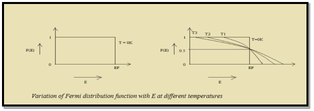
Case (i) Probability of occupation for E < EF at T = 0K

When T = 0K and E < EF, we have
F(E) =  =
=  = 1
= 1
Thus at T = 0K, there is 100 % chance for the electrons to occupy the energy levels below the Fermi level.
|
Figure 12: Fermi distribution
Case (ii) Probability of occupation for E>EF at T = 0K
When T = 0K and E > EF, we have
F(E) =  =
=  =
=  = 0
= 0
Thus, there is 0 % chance for the electrons to occupy energy levels above the Fermi energy level. From the above two cases, at T = 0K the variation of F(E) for different energy values becomes a step function.
Case (iii) Probability of occupation at ordinary temperature
At ordinary temperature, the value of probability starts reducing from 1 for values of E slightly less than EF. With the increase of temperature, i.e., T> 0K, Fermi function F (E) varies with E.
At any temperature other than 0K and E = EF
F(E) =  =
=  =
=  = 50%
= 50%
Hence, there is 50 % chance for the electrons to occupy Fermi level. Further, for E > EF the probability value falls off rapidly to zero.
Case (iv) At high temperature
When kT >> EF, the electrons lose their quantum mechanical character and Fermi distribution function reduces to classical Boltzmann distribution
Key Takeaways
- The Fermi function gives the probability of occupying an available energy state.
- Fermi-Dirac distribution function represents the probability of an electron occupying a given energy level at absolute temperature. It is given by

- At ordinary temperature, the value of probability starts reducing from 1 for values of E slightly less than EF. With the increase of temperature, i.e., T> 0K, Fermi function F (E) varies with E.
Intrinsic semiconductors—carrier concentration
Here we will calculate the number of electrons excited into conduction band at temperature T and also the hole concentration in the valence band. It is assumed that the electrons in the conduction band behave as if they are free particles with effective mass me* and the holes near the top of the valence band behave as if they are free particles with effective mass mh*.
Here we will calculate the electron concentration, hole concentration
Density of Electrons in Conduction Band
The number of free electrons per unit volume of semiconductor having energies in between E and E + dE is represented as N(E) dE
dE = width of Energy band
Therefore, we have:
N(E) dE = ge(E) dE fe(E) ……….(1)
ge(E) = The density of electron states per unit volume
fe(E) = Fermi-Dirac distribution function i.e. probability that an electron occupies an electron state
The number of electrons present in the conduction band per unit volume of material ‘n’ is obtained by integrating N(E) dE between the limits Ec and Ect
Where Ec = the bottom energy levels of conduction band
Ect = the bottom and top energy levels of conduction band
n =  ……….(2)
can be written as
n =  =
= 
n =  -
-  ……….(3)
we know that above Ect, there is no electrons.
Hence, Equation (3) becomes
n =  -
- 
n =  ……….(4)
The Fermi-Dirac distribution function fe(E) can be represented as:
 (E) =
(E) = ……….(5)
Compared to the exponential value, so the ‘1’ in the denominator can be neglected.
So  >>1
>>1
Hence,  (E) =
(E) = =
=  ……….(6)
The density of electron states ge(E) in the energy space from E = 0 to E can be written as:
 (E) =
(E) =  [
[ ]3/2 (E - 0) ½ ……….(7)
where me* is the effective mass of an electron and h is Planck’s constant.
 (E)dE =
  [
[ ]3/2 (E - 0) ½dE ……….(8)
To evaluate n, the density of states is counted from Ec, since the minimum energy state in conduction band is Ec. so eq (8) can become
 (E)dE =
  [
[ ]3/2 (E - Ec) ½dE ……….(9)
Substituting Equations (6) and (9) in (4) gives n = n = The above equation can be simplified by the following substitution: Put ɛ = E − Ec ………… (11) So, dɛ = dE In Equation (11), Ec is constant, as we change the variable E to ε in Equation (10), the integral limits also change. In Equation (11), as E → Ec then ε → 0 and E → ∞, then ε also → ∞. the exponential term in Equation (10) becomes:
Substituting Equations (11) and (12) in (10), we get: n = n = Above integral (I) can be simplified by substitution. Put ε = x2 so that dɛ = 2x dx I = = = Substituting Equation (14) in (13) gives: n = n = n = n = The term n =Nc
|
Density of Holes in Valence Band
The number of holes per unit volume of semiconductor in the energy range E and E + dE in valence band is represented as P(E) dE. Proceeding same way( as in case of electrons) we have
Therefore, we have:
P(E) dE = gh(E) dE fh(E) ……….(17)
dE = width of Energy band
gh(E) = The density of holes states per unit volume
fh(E) = Fermi-Dirac distribution function i.e. probability that an hole occupies an electron state
The number of electrons present in the conduction band per unit volume of material ‘n’ is obtained by integrating P(E) dE between the limits Evb and EV
where EV = the bottom energy levels of valence band
Evb = the bottom and top energy levels of valence band
The total number of holes present in the valence band per unit volume of material ‘p’ is obtained by integrating P(E) dE
Equation (18) can be represented as:
Now we know that below Evb no holes is present. Hence, Equation (19) becomes
|
We know hole can also be defined as absence of an electron.
presence of a hole = the absence of an electron
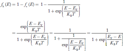
Hence, the Fermi-Dirac function of holes fh(E) in the valence band is:
Compared to exponential, the ‘1’ in the denominator is negligible, Hence,
The density of hole states between E and E + dE in valence band can be written similar to Equation (8.9) for electrons.
|
Where mh* is the effective mass of hole.
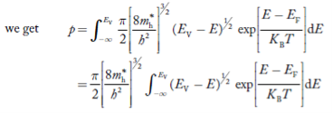
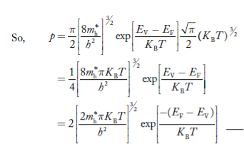
Substituting Equations (21) and (22) in (20),
|
The above equation can be simplified by the substitution:
Put ɛ = EV − E ............. (24)
so dɛ = − dE
In Equation (24), EV is constant, as we change the variable E to ε in Equation (23), the integral limits also change.
In Equation (24),
as E → EV then ε → 0
and E→ −∞, then ε → ∞
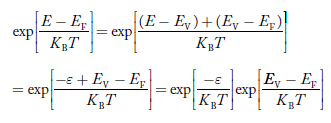
the exponential term in Equation (23) becomes:
Substituting Equations (24) and (25) in (23), we get:
From Equation (14), we know the integral value
….The term
|
Fermi Level
We know that in intrinsic semiconductor
Electron concentration ‘n’ = Hole concentration ‘p’
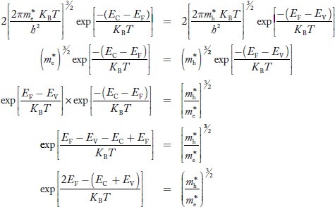
Equating Equations (15) and (27), we get
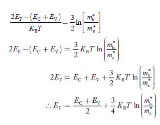
Taking logarithms on both sides, we get
|
Normally, mh* is greater than me*, since ln  is very small so that EF is just lie in the middle of energy gap
Temperature effect on Fermi level
Fermi level slightly rises with increase of temperature.
But in case of pure intrinsic semiconductor like Si and Ge,
mh* ≈ me*
So in these cases Fermi level lies at the middle of energy gap.
Law of Mass Action and Intrinsic Concentration (ni)
Law of Mass Action: the product of electron and hole concentration ia a constant at a given temperature and is equal to the square of Intrinsic Concentration (ni)2 . This is called Law of Mass Action. However, if impurity atoms are added to a semiconductor to increases n, there will be corresponding decrease in p such that the product np remains constant.
Thus we have np= (ni)2
- We know that electron-hole recombination take place inside a semiconductor, and also electron-hole pairs will be created due to thermal energies.
- The electron concentration and hole concentration remain constant as long as the temperature remains constant.
At temperature T K, in an intrinsic semiconductor n = p = ni,
Where ni is called intrinsic concentration.
Also the product np = ni2 ……………(30)
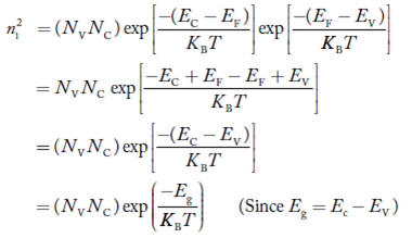
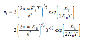
Substituting Equations (16) and (28) in (30) gives
Also substituting Equations (15) and (27) in (30) gives
If me* = mh* = m, where m is the rest mass of an electron, then Equation (32) becomes
Where
|
For pure Ge at 300 K, the intrinsic electron concentration is about 2.4 x 10¹⁹ m-3 when the concentration of germanium atoms is 4.4 x 1028 m-3. This shows that at ordinary temperature, only about two covalent bonds per 109 atoms of germanium are broken and contribute to intrinsic conductor. Whereas in metals such as copper, about 1028 electrons per cubic metre are available for conduction.
Key Takeaways
- The density of Electrons in Conduction Band
n =Nc
- The density of Holes in Valence Band

- Fermi level slightly rises with an increase of temperature. But in the case of a pure intrinsic semiconductor like Si and Ge, mh* ≈ me*, So in these cases, the Fermi level lies in the middle of the energy gap.
- The product of electron and hole concentration is a constant at a given temperature and is equal to the square of Intrinsic Concentration (ni)2 .
The relationships established an explicit dependence on the dopant concentrations introduced into a semiconductor. It is the charge neutrality relationship that provides the general tie between the carrier and dopant concentrations.
To establish the charge neutrality relationship. Let us consider a uniformly doped semiconductor. Systematically examining little sections of the semiconductor far from any surfaces, and assuming equilibrium conditions prevail, one must invariably find that each and every section is charge-neutral, it, contains no net charge. If this were not the case, electric fields would exist inside the semiconductor.
The electric fields in turn would give rise to carrier motion and associated currents—a situation totally inconsistent with the assumed equilibrium conditions.
There are, however, charged entities inside all semiconductors. Electrons, holes, ionized donors (donor atoms that have become positively charged by donating an electron to the conduction band) and negatively-charged ionized acceptors an all exist simultaneously inside any given semiconductor.
For the uniformly doped material to be everywhere charge-neutral require
or
|
Where, by definition.
 = Number of ionized (positively charged) donors/cm3.
 = Number of ionized (negatively charged) acceptors/ cm3.
There is sufficient thermal energy available in a semiconductor at room temperature to ionize almost all of the shallow-level donor and acceptor sites.
Defining
ND = total number of donors/ cm3.
NA = total number of acceptors/ cm3
and setting
 = ND
= ND
 = NA
= NA
We obtain
 …………. (3)
This assumes total ionization of dopant atoms. Equation (3) is the standard forms of the charge neutrality relationship.
Key Takeaways
- The charge neutrality relationship that provides the general tie between the carrier and dopant concentrations.
- Systematically examining little sections of the semiconductor far from any surfaces, and assuming equilibrium conditions prevail, one must invariably find that each and every section is charge-neutral, it, contains no net charge.
- The standard forms of the charge neutrality relationship is given by

Carrier Concentration in Extrinsic Semiconductors
The number of charge carriers present per unit volume of a semiconductor material is called carrier concentration.
Suppose donor and acceptor atoms are doped in a semiconductor.
At temperature T K,
n = number of conduction electrons
p = number of holes
N−A = number of acceptor ions
N+D = number of donor ions
We know that the below equation holds good in semiconductor. The total negative charge due to conduction electrons and acceptor ions is equal to holes and donor ions in unit volume of material.
So the material will be considered neutral if,
n + N−A = p + N+D ……….(34)
Equation (34) is called charge neutrality equation.
In the above equation
concentration of acceptor ions N−A = acceptor concentration x probability of finding an electron in acceptor level
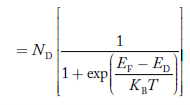
Similarly, the donor ions concentration is
|
In n-type material
Note
nn represents electrons in n-type material
pn represents holes concentration in n-type material.
there are no acceptor atoms so N−A = 0.
At 0 K, all the electron states in donor level are occupied by electrons.
As the temperature is increased from 0 K, some of the electrons jump from these donor states into the conduction band.
Also the concentration of holes is extremely less compared with the concentration of conduction electrons [p << n]
From Equation (34) we have
n = p N+D
(Or) n ≈ N+D …………(38) [since p << N+D]
At temperature T K,
As the temperature increase Almost all the donor atoms donate electrons to conduction band.
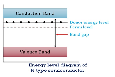
|
Figure 13: Energy Level diagram of N type Semiconductor
So, in n-type material, the free electron concentration is almost equal to the donor atoms.
So we can rewrite the above equation as
nn ≈ ND …………….(39)
where nn represents electrons in n-type material
also the hole concentration in n-type material can be obtained by applying law of mass action nn pn =ni2
 …………..(40)
where pn represents holes concentration in n-type material.
In n-type material at 0 K, the Fermi energy level lies in the middle of Ec and ED

At temperature> 0K
 ……….(41)
With increase in temperature the Fermi level shifts upwards according to Equation (61) slightly due to ionization of donor atoms.
With further increase of temperature, electron-hole pairs are generated due to the breaking of covalent bonds, hence Fermi level shifts downwards.
In p-type semiconductor
Note
pp represents holes in p-type material
np represents electrons in p-type material
There are no donor atoms so means no ions present  = 0.
= 0.
At 0 K, all the acceptor levels are not occupied by electrons.
As the temperature is increased from 0 K, some electrons jump from top valence band energy levels to the acceptor states, leaving holes in the valence band and acceptor ions  are formed.
At some room temperature T K, concentration of conduction electrons is extremely less compared with hole concentration.
∴ From Equation (34), we have
n + N−A = p ……………(42)
(or) N−A ≈ p ……………. (43) [since n << N−A]
At temperature T K, in p-type material,
the hole concentration is almost equal to the acceptor atoms in unit volume of the material.
So, Equation (43) can be written as
pp ≈ NA ……………….(44)
where pp represents holes in p-type material
The electron concentration in p-type material can be obtained by applying law of mass action as nppp = ni2
 …………….(45)
where np represent free electron concentration in p-type material.
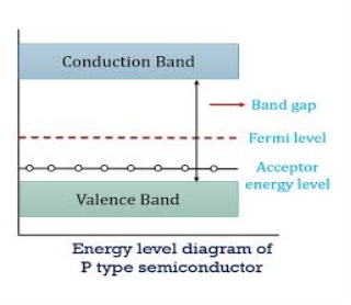
|
Figure 14: Energy Level diagram of P- type Semiconductor
In p-type material, the Fermi level lies in between EV and EA at 0 K

As the temperature is increased from 0 K, the Fermi level shifts downwards slightly as per Equation (46) due to ionization of acceptor atoms.
And with further increase of temperature, electron-hole pairs are generated due to the breaking of covalent bonds, so Fermi level shifts upwards.
Key Takeaways
Carrier Concentration in Extrinsic Semiconductors
- The donor ions concentration is
- Concentration of acceptor ions N−A

- Fermi Level shifts in case of extrinsic semiconductor.
1.10.1 DRIFT
Drift is charged-particle motion in response to an applied electric field.
Within semiconductors the drifting motion of the carriers on a microscopic scale can be described as follows: When an electric field (Si) is applied across a semiconductor as visualized in figure 15(a) the resulting force on the carriers tends to accelerate the +q charged holes in the direction of the electric field and the — q charged electrons in the direction opposite to the electric field. Because of collisions with ionized impurity atoms and thermally agitated lattice atoms, however, the carrier acceleration is frequently interrupted (the carriers are d to be scattered). The net result, pictured in Figure 15(b), is carrier motion generally along the direction of the electric field, but in a disjointed fashion involving repeated periods of acceleration and subsequent decelerating collisions.
|
Figure 15: Visualization of carrier drift: (a) motion of carriers within a biased semiconductor bar (b) drifting hole on microscopic or atomic state (c) carrier drift on a macroscopic state.
The microscopic drifting motion of a single carrier is difficult to analyse as it is complex however the measurable quantities are macroscopic observables that gives the average or overall motion of the carriers.
Averaging over all electrons or holes at any given time, we find that the resultant motion of each carrier type can be described in terms of a constant drift velocity, vd
In other words, on a macroscopic scale, drift may be visualized as nothing more than all carriers of a given type moving along at a constant velocity in a direction parallel or antiparallel to the applied electric field.
It is important to point out that the drifting motion of the carriers arising in response to an applied electric field is actually superimposed upon the always-present thermal motion of the carriers. Electrons in the conduction band and holes in the valence band gain and lose energy via collisions with the semiconductor lattice and are nowhere near stationary even under equilibrium conditions. In fact under equilibrium conditions the thermally related carrier velocities average  1/1000 the speed of light at room temperature.
However, the thermal motion of the carriers is completely random. Thermal motion therefore averages out to zero on a macroscopic scale, does not contribute to current transport, and can be conceptually neglected.
1.10.2 MOBILITY
The drift velocity produced per unit electric field is called 'mobility' , Thus Mobility is obviously a central parameter in characterizing electron and hole transport due to drift.
μ =  or μE =
The word mobility refers to freedom of movement. Analogously, in semiconductor work the mobility parameter is a measure of the ease of carrier motion in a crystal. Increasing the motion-impeding collisions within a crystal decreases the mobility of the carriers.
In other words, the carrier mobility varies inversely with the amount of scattering taking place within the semiconductor.
Lattice scattering involving collisions with thermally agitated lattice atoms, and ionized impurity (i.e., donor-site and/or acceptor-site) scattering. Relative to lattice scattering, it should be emphasized that it is the thermal vibration, the displacement of lattice atoms from their lattice, positions, that leads to carrier scattering. The internal field associated with the stationary array of atoms in a crystal is already taken into account in the effective mass formulation.
μ = q /m*
/m*
where  is the mean free time between collisions and m* is the conductivity effective mass.
However, μ is also noted to vary inversely with the carrier effective mass—lighter carriers move more readily.
The carrier mobilities are essentially independent of the doping concentration. For dopings in excess of l015/cm3, the mobilities monotonically decrease with increasing NA or ND.
The mobilities of carrier depend upon temperature as μ 
 . For Electrons μe
 and for holes μp

1.10.3 RESISTIVITY
Resistivity is an important material parameter that is closely related to carrier drift. Qualitatively, resistivity is a measure of a material's inherent resistance to current flow—a "normalized" resistance that does not depend on the physical dimensions of the material.
Quantitatively, resistivity (p) is defined as the proportionality constant between the electric field impressed across a homogeneous material and the total particle current per unit area flowing in the material; that is,
E =ρJ ………… (1)
Or
J = E =  ………… (2)
where = 1/ρ is the material conductivity. In a homogeneous material J= Jdrift and as established with the help of Eqs. (1) and (2), it therefore follows that
Jdrift = JN(drift) + JP(drift) ………… (3)
 =
=  ………… (4)
In a non-degenerate donor-doped semiconductor maintained in the extrinsic temperature region where ND >> ni, ni  ND and p = ni2/ND << n.
Thus, for typical dopings and mobilities,  =
=  ND in an n-type semiconductor. Similar arguments yield
  =
=  NA in a p-type semiconductor. Consequently, under conditions normally encountered in Si samples maintained at or near room temperature, Eq. (3.7) simplifies to
 =
=  for n-type semiconductor
and
 =
=  for p-type semiconductor.
One of the most common methods of measuring a material‘s surface resistivity is using either the two-or four-point probe method .Two probe method is used to measure the resistivity of films with fairly large resistance. But if the film resistance is very small (comparable with the lead) four probe method is adopted.
Both two and four probe methods are the most popular methods for measuring resistivity due to the ability of minimizing the parasitic effects of contact resistance, Rc shown below in equation (1). Let us illustrate four probes method
|
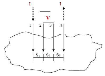
Figure 16: Four-point probe test setup. Probes 1 and 4 carry current (I), 2 and 3 measure voltage (V).
In the four-point probe setup as shown in figure 16, the voltage potential V adjacent to a probe carrying current can be given by:
V = ρI/ 2πr ………….(2)
where ρ is the surface resistivity of a material of semi-infinite size, I is the current in the probe, and r is the distance between the voltage measurement and the current probe.
A very convenient way to measure the sheet resistance of a film is to press a 4-point metal tip probe assembly in to the surface as shown in (figure 2). The outer probe is connected to current source and inner probes to detect the voltage drop.
Voltage at probe number 2 is
Voltage at probe number 3 is
Hence the total voltage is V
The resistivity
If all the probes are equidistant with inner probe distance S then the equation reduces to
|
Most surface resistivity measurements of semiconductor wafers or thin films are made on a small surface area substrate. Small spacing differences in probe spacing can cause the resistivity values to vary widely across a sample surface. A high quality four-point head is necessary to get repeatable and reliable resistivity values. When measuring samples with low resistivity, high currents are needed in the current probes to obtain good voltage readings.
1.10.4 DRIFT CURRENT, DIFFUSION CURRENT, TOTAL CURRENT
Drift current and diffusion currents
In case of semiconductors, we observe two kinds of currents.
- Drift current
- Diffusion current
Drift current Definition: - The flow of electric current due to the motion of charge carriers under the influence of external electric field is called drift current.
When an electric field E is applied across a semiconductor material, the charge carriers attain a drift velocity vd
So drift velocity vd =μ.E
The relation between current density J and drift velocity vd is
J = Nqvd
Where N is the carrier concentration
q is the charge of electron or hole
From equations (1) and (2), we get
Jdrift = NqμE
μ is the mobility of charge carrier.
The above equation shows the general expression for drift current density. Drift current density due to electrons is
Je(drift) = neμeE
Where n is the electrons carrier concentration
and μe is the mobility of electrons.
Drift current density due to holes is
Jh(drift) = peμhE
Where p is the carrier concentration of holes.
μh is the mobility of holes
so Total drift current density
Jdrift (total) = Je(drift) + Jh(drift) = neμeE + peμhE
= eE (nμe+pμh )
Diffusion current
Diffusion is a process whereby particles tend to spread out or redistribute as a result of their random thermal motion, migrating on a macroscopic scale from regions of high particle concentration into regions of low particle concentration. If allowed to progress unabated.
The diffusion process operates so as to produce a uniform distribution of particles. The diffusing entity, it should be noted, need not be charged; thermal motion, not antiparticle repulsion, is the enabling action behind the diffusion process.
In semiconductors the diffusion process on a microscopic scale in similar so that occurring in the hypothetical system, the random motion of the diffusing particles is three-dimensional and not “compartmentalised.” On a macroscopic scale the net effects of diffusion is precisely she same within both the hypothetical system and semiconductors; there is an overall migration of particles from a region of concentration to the region of low particle concentration Within semiconductors the electrons and holes are charged, and diffusion-current carrier transport therefore given rise to particle currents as shown in figure.
|
Figure 17: Diffusion at macroscopic level
Definition: -The flow of electric current due to the motion of charge carriers under concentration gradient is called diffusion current
Or
The motion of charge carriers from the region of higher concentration to lower concentration leads to a current called diffusion current.
Let ∆N be the excess electron concentration. Then according to Fick’s law, the rate of diffusion of charge carriers is proportional to concentration gradient
Rate of diffusion of charge ∝ -
= - D
Where D is the diffusion coefficient of charge carriers.
The negative sign indicates decrease of N with increase of x So,
the diffusion current density Jdiffu is
Jdiffu = - qD
Where q is the charge of the charge carrier
Diffusion current density due to holes is
Jdiffu (hole) = - eDh
Diffusion current density due to electrons is (as electron carry negative charge so we will get +sign here.
Jdiffu (electrons) = eDe
Jdiffu (total) = Jdiffu (hole) + Jdiffu (electrons)
Jdiffu (total) = - eDh + eDe
+ eDe
The expression for total current density due to holes is
Jh (total) = Jh(drift) + Jdiffu (hole) = peμhE - eDh
The expression for total current density due to electrons is
Je (total) = Je(drift) + Jdiffu (electrons) = neμeE + eDe
Key Takeaways
- Drift is charged-particle motion in response to an applied electric field.
- The drift velocity produced per unit electric field is called 'mobility'
- Resistivity is a measure of a material's inherent resistance to current flow—a "normalized" resistance that does not depend on the physical dimensions of the material.
- In case of semiconductors we observe two kinds of currents; Drift current and Diffusion current.
- The flow of electric current due to the motion of charge carriers under the influence of external electric field is called drift current. Total drift current density is given by Jdrift (total) = Je(drift) + Jh(drift) = eE (nμe+pμh )
- The flow of electric current due to the motion of charge carriers under concentration gradient is called diffusion current. Total current density due to electrons is given by Je (total) = Je(drift) + Jdiffu (electrons) = neμeE + eDe

Einstein Relationship
The formula between the D's and the μ's known as the Einstein relationship.
To simplify the development, we consider one dimensional system. The sample under analysis is taken to be a non-degenerate, non-uniformly doped semiconductor maintained under equilibrium conditions.
The net carrier currents must be identically zero under equilibrium conditions, and focusing on the electrons, we can state
However,
and
Moreover, with dEF/dx=0 (due to the positional invariance of the Fermi level under equilibrium conditions),
Substituting dn/dx from Eq. (4) into Eq. (1) and rearranging the result slightly. one obtains
Since
The above equation (6) is known as Einstein Relationship for electrons. This equation hold for holes also
|
The above equation (7) is known as Einstein Relationship for holes.
Although it was established while assuming equilibrium conditions, we can present more elaborate arguments that show the Einstein relationship to be valid even under non-equilibrium conditions.
The non-degenerate restriction however, still applies: slightly modified forms of Eqs. (7) result when the argument is extended to degenerate materials.
For Example
Relative to numerical values, note that kT/q is a voltage, and at room temperature (300 K) is equal to 0.0259V.
Hence, for an ND = 1014/cm3 Si sample maintained at room temperature,
DN = (kT/q) μn = (0.0259)(1358 cm2 /N-sec) = 35.2 cm2 /sec
Key Takeaways
- The formula between the D's and the μ's known as the Einstein relationship.
- Einstein Relationship for electrons

- Einstein Relationship for holes.

1.12.1 RECOMBINATION-GENERATION
Carrier generation is a process where electron-hole pairs are created by exciting an electron from the valence band of the semiconductor to the conduction band, thereby creating a hole in the valence band.
Recombination is the reverse process where electrons from the conduction and holes from valence band recombine and are annihilated.
These processes must conserve both quantized energy and momentum, and the vibrating lattice plays a large role in conserving momentum.
- Recombination and generation are always happening in semiconductors both optically and thermally.
- Their rates are in balance at equilibrium.
- If the product of the rate becomes greater than the recombination rate, again driving the system back towards equilibrium.
- As the electron and hole densities is a constant at equilibrium, maintained by recombination and generation occurring at equal rates.
- When there is a surplus of carriers the rate of recombination becomes greater than the rate of generation, driving the system back towards equilibrium.
In semiconductors several different processes exist which lead to recombination, the most important ones are:
1) Band-to-band recombination
2) R-G centres,
3) Auger and impact ionization.
1.12.2 BAND-TO-BAND RECOMBINATION OR RADIATIVE RECOMBINATION
Band-to-band recombination or Radiative recombination is the reverse process of photon absorption, where an electron drops back down to its equilibrium energy band and radiates a photon.
It is the process of electrons jumping down from the conduction band to the valence band in a radiative manner.
During band-to-band recombination the energy absorbed by a material is released in the form of photons. Generally, these released photons contain the same or less energy than those initially absorbed.
|
Figure 18: Band-to-band recombination
The photon emitted may have the energy of the band gap difference or less, depending on how much energy is lost in the mechanism
Radiative recombination plays a more major role in direct band semiconductors.
The total radiative recombination rate, given below as R, is proportional to the product of the concentration of occupied states (electrons, n) in the conduction band and that of the unoccupied states in the valence band (holes, p)
R= Bnp
Band-to-band recombination depends on the density of available electrons and holes. Both carrier types need to be available in the recombination process. Therefore, the rate is expected to be proportional to the product of n and p. Also, in thermal equilibrium, the recombination rate must equal the generation rate since there is no net recombination or generation. As the product of n and p equals ni2 in thermal equilibrium, the net recombination rate can be expressed as:
U= B(np-ni2)
where B is the bimolecular recombination constant for a given semiconductor. It can be calculated from the semiconductor’s absorption coefficient. ni2 is the familiar “intrinsic carrier concentration”
1.12.3 R—G CENTER
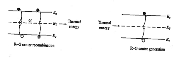
Recombination involves a "third party," or intermediary, and takes place only at special locations within the semiconductor known as R—G centres.
Recombination at an R—G centre is a two-step process. First, one type of carrier, say an electron, strays into the vicinity of an R—G centre, is caught by the potential well associated with the centre, loses energy, and is trapped. Subsequently, a hole conies along, is attracted to the trapped electron, loses energy, and annihilates the electron within the centre. Alternatively, one can think of the electron as losing energy a second time and annihilating the hole in the valence band. R—G centre recombination, also called indirect recombination, typically releases thermal energy (heat) during the process or, equivalently, produces lattice vibrations.
|
Figure 19: R—G Centre
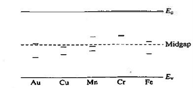
R—G centres are lattice defects or special impurity atoms such as gold in Si. Lattice defects and the special atoms in the form of unintentional impurities are present even in semiconductors of the highest available purity. The R—G centre concentration, however, is normally very low compared to the acceptor and donor concentrations in device-quality materials. The most important property of the R—G centres is the introduction of allowed electronic levels near the centre of the band gap. These levels are identified by the ET energy label in Figure 19. The near mid-gap positioning of the levels is all-important because it distinguishes R-G centres from donors and acceptors. The mid-gap levels introduced by select R—G centre impurities in Si are summarized in Figure 20.
|
Figure 20: mid-gap levels introduced by select R—G centre impurities in Si
1.12.4 AUGER RECOMBINATION AND IMPACT IONIZATION
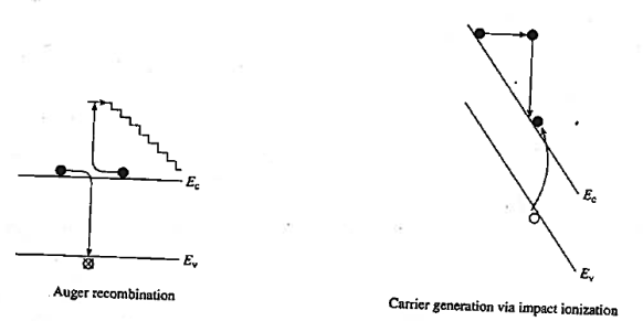
Another non-radiative recombination is Auger recombination, it is given off in the form of kinetic energy to another electron. The energy that becomes available through electron-hole recombination (Eg) is dissipated by the excitation of a free electron high into the conduction band, or by a hole deeply excited into the valence band. The highly excited carrier will subsequently lose energy by multiple phonon emission until they are close to the band edge. Recombination rate due to the Auger process
RAuger = Cpnp2 (22)
RAuger = Cnn2p (23)
Auger recombination reduces the luminescence efficiency in semiconductors only at very high excitation intensity or at very high carrier injection currents. At lower carrier concentrations, the Auger recombination rate is very small and can be neglected.
Auger recombination involves three particles: an electron and holes, which recombine in a band-to-band transition and give off the resulting energy to another electron or hole. The expression for the net recombination rate is therefore similar to that of band-to-band recombination but includes the density of the electrons or holes, which receive the released energy from the electron-hole annihilation.
|
Figure 21: Auger recombination and Impact ionization
As shown in figure Auger Recombination is band-to-band recombination occurs simultaneously with the collision between two like carriers. The energy released by the recombination is transferred during the collision to the surviving carrier. This highly energetic carrier subsequently "thermalizes" —loses energy in small steps through heat-producing collisions with the semiconductor lattice. The "staircase" in Figure represents the envisioned stepwise loss of energy.
In other words, Auger recombination, the energy is given to a third carrier which is excited to a higher energy level without moving to another energy band.
After the interaction, the third carrier normally loses its excess energy to thermal vibrations. Since this process is a three-particle interaction, it is normally only significant in non-equilibrium conditions when the carrier density is very high.
Auger recombination is most important at high carrier concentrations caused by heavy doping. In silicon-based solar cells, Auger recombination limits the lifetime and ultimate efficiency.
The more heavily doped the material is, the shorter the Auger recombination lifetime.
Impact ionization, the inverse of Auger recombination, is visualized in Figure 21. In this process an electron–hole pair is produced as a result of energy released when a highly energetic carrier collides with the crystal lattice. The generation of carriers through impact ionization routinely occurs in the high -field regions of devices. We will see this process when treating breakdown in pn junctions.
Key Takeaways
- Carrier generation is a process where electron-hole pairs are created by exciting an electron from the valence band of the semiconductor to the conduction band, thereby creating a hole in the valence band.
- Recombination is the reverse process where electrons from the conduction and holes from valence band recombine and are annihilated.
- These processes must conserve both quantized energy and momentum, and the vibrating lattice plays a large role in conserving momentum.
- Recombination and generation are always happening in semiconductors both optically and thermally. Their rates are in balance at equilibrium.
- In semiconductors several different processes exist which lead to recombination, the most important ones are: Band-to-band recombination,
R-G centres, Auger and impact ionization.
- Recombination involves a "third party," or intermediary, and takes place only at special locations within the semiconductor known as R—G centers.
- Auger recombination involves three particles: an electron and a hole, which recombine in a band-to-band transition and give off the resulting energy to another electron or hole.
- Impact ionization, the inverse of Auger recombination
Equations of state
We have studied separately modelled the primary types of carrier action taking place inside semiconductors. Within actual semiconductors all the various types of carrier action occur at the same time, and the state of any semiconductor can be determined only by taking into account the combined effect of the individual types of carrier action. "Putting it all together leads to the basic set of starting equations employed in solving device problems known as the equations of state.
Continuity Equations
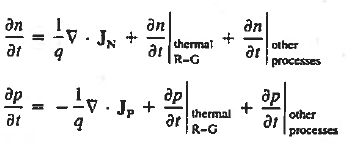
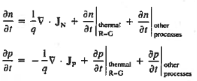
Each and every type of carrier action—whether it be drift, diffusion, indirect or direct thermal recombination, indirect or direct generation, or some other type of carrier action—gives rise to a change in the carrier concentrations with time. The combined effect of all types of carrier action can therefore be taken into account by equating the overall change in the carrier concentrations per unit time  or
or  to the sum of the time
  or
or  due to the individual processes; that is,
|
The overall effect of the individual processes is established by applying the requirement of conservation of carriers. Electrons and holes cannot mysteriously appear and disappear at a given point, but must be transported to or created at the given point via some type of on-going carrier action. There must be a spatial and time continuity in the carrier concentrations.
For this reason, Eqs. (1) are known as the continuity equations. The continuity equations can be written in a somewhat more compact form by noting
|
Equations (2), which can be established by a straightforward mathematical manipulation, merely state that there will be a change in the carrier concentrations within a given small region of the semiconductor if an imbalance exists between the total carrier currents into and out of the region.
Using Eqs. (2), we obtain
|
The (3) continuity equations are completely general and directly or indirectly constitute the starting point in most device analyses.
In computer simulations the continuity equations are often employed directly. The continuity equations are typically utilized only in an indirect fashion.
Key Takeaways
- Each and every type of carrier action—whether it be drift, diffusion, indirect or direct thermal recombination, indirect or direct generation, or some other type of carrier action—gives rise to a change in the carrier concentrations with time
- Continuity equations are completely general and directly or indirectly constitute the starting point in most device analyses. It is given as
|
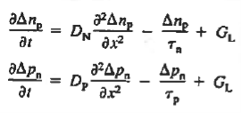
The "workhorse" minority carrier diffusion equations are derived from the continuity equations by invoking the following set of simplifying assumptions:
(I) The particular system under analysis is one-dimensional; i.e., all variables are at most a function of just one coordinate (say the x-coordinate).
(2) The analysis is limited or restricted to minority carriers.
(3) =0 in the semiconductor or regions of the semiconductor subject to analysis.
(4) The equilibrium minority carrier concentrations are not a function of position. In other words, n0  n0(x), p0
  p0(x)
p0(x)
(5) Low-level injection conditions prevail.
(6) Indirect thermal recombination—generation is the dominant thermal R—G mechanism.
(7) There are no "other processes," except possibly photo generation, taking place within the system.
Working on the continuity equation for electrons, we note that
if the system is one-dimensional. Moreover,
when = 0 and one is concerned only with minority carriers. The drift component can be neglected in the current density expression because is small by assumption and minority carrier concentrations are also small, making the n product extremely small. Since by assumption n0
Combining Eqs. (1) through (3) yields
Turning to the remaining terms in the continuity equation for electrons, the assumed dominance of recombination—generation via R—G centers, combined with the low-level injection and minority canter restrictions, allows us to replace the thermal R—G term as
In addition, apply (7) yeilds
where it is understood that GL = 0 if the semiconductor is not subject to illumination. Finally, the equilibrium electron concentration is never a function of time, n0
Substituting Eqs. (4) through (7) into the continuity equation, and simultaneously recording the analogous result for holes, one obtains
|
This is known as Minority carrier diffusion equations. The equations are valid only for minority carriers, applying to electrons in p-type materials and to holes in n-type materials.
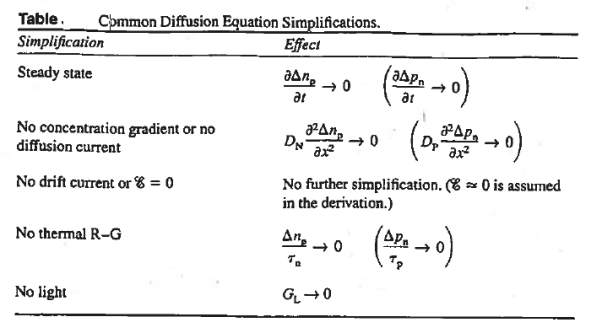
Common Diffusion Equation simplification is given below
|
Figure 22: Common Diffusion Equation simplification
Key Takeaways
- The "workhorse" minority carrier diffusion equations are derived from the continuity equations by invoking the following set of simplifying assumptions
- The Minority carrier diffusion equations are given as

- The equations are valid only for minority carriers, applying to electrons in p-type materials and to holes in n-type materials.
References
- Semiconductor Device Fundamentals by Robert F. Pierret
- Physics of Semiconductor Devices by S.M. Sze.
.
