UNIT-3
PHYSICS AND TECHNOLOGIES OF BJT
Bipolar junction transistor or BJT is simply known as Transistor. A transistor consists of two pn junctions formed by sandwiching either p-type or n-type semiconductor between a pair of opposite types.
The prefix 'trans' means the signal transfer property of the device while 'istor ' classifies it as a solid element in the same general family with resistors. Accordingly there are two types of transistors
- n-p-n transistor
- p-n-p transistor
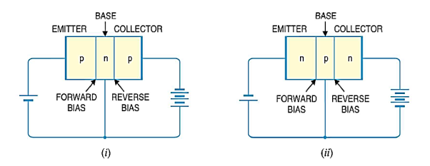
An n-p-n transistor is composed of two n-type semiconductors separated by a thin section of p-type as shown in Figure 1 (i).
However, a p-n-p transistor is formed by two p-sections separated by a thin section of n-type as shown in Figure 1(ii).
|
Figure1: (i) n-p-n transistor (ii) p-n-p transistor
In each type of transistor, the following points may be noted:
(i) Transistor may be regarded as a combination of two diodes connected back to back.
(ii) There are three terminals, one taken from each type of semiconductor.
(iii) The middle section is a very thin layer. The thin layer plays an important role in the function of a transistor.
A transistor has two pn junctions. one junction is forward biased and the other is reverse biased. The forward biased junction has a low resistance path whereas a reverse biased junction has a high resistance path. The weak signal is introduced in the low resistance circuit and output is taken from the high resistance circuit. Therefore, a transistor transfers a signal from a low resistance to high resistance.
A transistor (pnp or npn) has three sections of doped semiconductors. The section on one side is the emitter and the section on the opposite side is the collector. The middle section is called the base and forms two junctions between the emitter and collector.
|
Figure 2: (i) p-n-p transistor (ii) n-p-n transistor
Emitter: The section on one side that supplies charge carriers (electrons or holes) is called the emitter. The emitter is always forward biased w.r.t. base so that it can supply a large number of majority carriers. In Figure 2 (i), the emitter (p-type) of pnp transistor is forward biased and supplies hole charges to its junction with the base. Similarly, in Figure 2 (ii), the emitter (n-type) of npn transistor has a forward bias and supplies free electrons to its junction with the base.
Collector: The section on the other side that collects the charges is called the collector. The collector is always reverse biased. Its function is to remove charges from its junction with the base. In Figure 2 (i), the collector (p-type) of pnp transistor has a reverse bias and receives hole charges that flow in the output circuit. Similarly, In Figure 2 (ii), the collector (n-type) of npn transistor has reverse bias and receives electrons.
Base: The middle section which forms two pn junctions between the emitter and collector is called the base. The base emitter junction is forward biased allowing low resistance for the emitter circuit. The base-collector junction is reverse biased and provides high resistance in the collector circuit.
Before studying action of transistor, some important facts about transistor should be keep in mind.
- The transistor has two pn junctions i.e. it is like two diodes. The junction between emitter and base may be called emitter-base diode or simply the emitter diode. The junction between the base and collector may be called collector-base diode or simply collector diode.
- The emitter diode is always forward biased whereas collector diode is always reverse biased.
- Three regions of transistor are emitter, base and collector. The base is much thin as compared to emitter while "collector is wider than both. To keep it simple it is assumed emitter and collector is considered to be of same size.
- The emitter is heavily doped so that it can inject a large number of charge carriers (electrons or holes) into the base. The base is lightly doped and very thin it passes most of the emitter injected charge carriers to the collector. The collector is moderately doped.
- The resistance of emitter diode (forward biased) is very small as compared to collector diode (reverse biased). Therefore, forward bias applied to the emitter diode is generally very small whereas reverse bias on the collector diode is much higher.
Working of Transistor
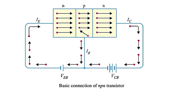
(i) Working of npn transistor: As discussed in the npn transistor emitter-base junction is forward biased to emitter-base junction and collector-base junction is reverse biased. The forward bias causes the electrons in the n-type emitter to flow towards the base. This constitutes the emitter current Ie.
Ie = Ib + Ic
|
Figure 3: n-p-n transistor
As these electrons flow through the p-type base, they tend to combine with holes. As the base is lightly doped and very thin, therefore, only a few electrons (less than 5%) combine with holes to constitute base current Ib. The remainder i.e. more than 95% cross over into the collector region to constitute collector current Ic In this way, almost the entire emitter current flows in the collector circuit. It is clear that emitter current is the sum of collector and base currents i.e.
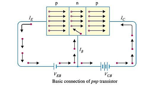
(ii) Working of pnp transistor: In the pnp transistor emitter-base junction is forward biased to emitter-base junction and collector-base junction is reverse biased. The forward bias causes the holes in the p-type emitter to flow towards the base. This constitutes the emitter current Ie. As these holes cross into n-type base, they tend to combine with the electrons. As the base is lightly doped and very thin, therefore, only a few holes (less than 5%) combine with the electrons.
|
Figure 4: p-n-p transistor
The remainder (more than 95%) cross into the collector region to constitute collector current Ic. In this way, almost the entire emitter current flows in the collector circuit. It may be noted that current conduction within pnp transistor is by holes. However, in the external connecting wires the current is still by electrons.
Thus the input circuit (i.e. emitter-base junction) has low resistance because of forward bias whereas output circuit (i.e. collector base junction) has high resistance due to reverse bias. As we have seen, the input emitter current almost entirely flows in the collector circuit. Therefore a transistor transfers the input signal current from a low resistance circuit to a high-resistance circuit.
Transistor’s Configuration:-
1) Common Base configuration(C.B)
2) Common emitter Configuration(C.E)
3) Common Collector Configuration(C.C)
COMMON BASE CONFIGURATION
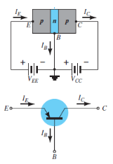
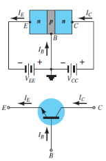
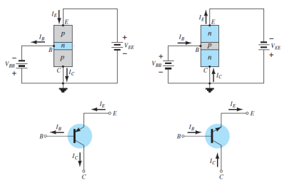
The notation and symbols of pnp and npn transistors are given below:
|
Figure 5: PNP CB and NPN CB (Ref. 2)
Here the base is common to both the input and output sides of the configuration.
The flow of holes will govern the direction of current.
Hence, Ic = Ib + Ie
Where Ic, Ib, Ie are the collector, base and emitter currents respectively.
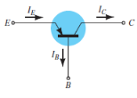
The graphical symbol of the PNP common base configuration is
|
Figure 6 : PNP common base(Ref. 2)
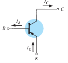
The arrow in the above symbol shows the direction of emitter current in the device.
Now, to study the behavior of the device we require two characteristics:
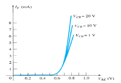
Input Characteristic Curve
|
Figure 7: Input Characteristic Curve (Ref. 2)
- It is the relation between the input current IE to the input voltage VBE for various levels of output voltage VCB.
- It is also known as driving point characteristics.
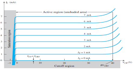
Output Characteristic Curve
|
Figure 8: Output Characteristic Curve (Ref. 2)
- It is the relation between the output current IC to the output voltage VCB for various levels of input current IE.
- It is also known as collector set of characteristics.
- It has three basic regions:
- Active Region
Here, base-emitter junction is forward biased and collector-base junction is reverse biased.
As input current IE increases above zero, output current IC increases to a magnitude equal to IE as determined by the basic transistor current relationship.
So the first approximation determined by the curve is
IC ≈ IE
2. Cut-off Region
It is defined as the region where the collector current IC is equal to 0A.
Here, the base-emitter junction and the collector-base junction both are in reverse bias.
3. Saturation Region
It is the region that lies towards the left of VCB = 0V.
Here, the base-emitter junction and the collector-base junction both are in forward bias.
COMMON EMITTER CONFIGURATION
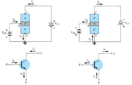
The notation and symbols of npn and pnp transistors are given below:
|
Figure 9: NPN CE and PNP CE (Ref. 2)
In the above figure all the currents are shown in their actual conventional directions.
The current relation developed earlier is still applicable,
IE = IB + IC
Where IE , IB , IC are the collector, base and emitter currents respectively.
The graphical symbol of the PNP common emitter configuration is
|
Figure 10: PNP common emitter (Ref. 2)
Now, to study the behavior of the device we require two characteristics:
Input Characteristic Curve
|
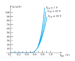
Figure 11: Input Characteristic Curve (Ref. 2)
It is the graph between the input current IB to the input voltage VBE for a range of values of output voltage VCE.
Note that the magnitude IB of is in micro amperes and that of IC is in milli amperes.
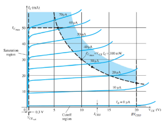
Output Characteristic Curve
|
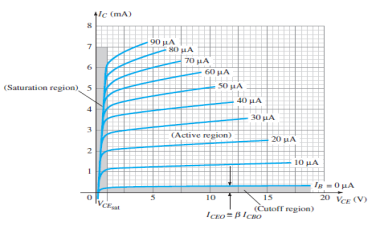
Figure 12: Output Characteristic Curve (Ref. 2)
It is the graph between the output current IC to the output voltage VCE for a range of values of input current IB.
It has three basic regions:
Active Region
- Here, the base-emitter junction is forward biased and collector base junction is reverse biased.
- These are the same conditions that existed in the active region of the common base configuration.
- This can be employed for voltage, current or power amplification.
Cut-off Region
- Here IC is not equal to zero when IB is zero.
- For linear amplification purposes, it is defined as IC = ICEO .
- The region below IB = 0µA is to be avoided for undistorted output signal.
- When the transistor is used as a switch, the condition should be ideally IC = 0mA for a chosen VCE voltage.
Saturation Region
- It is the region that lies towards the left of VCE = 0V.
COMMON COLLECTOR CONFIGURATION
The notation and symbols of npn and pnp transistors are given below:
|
Figure 13: NPN CC and PNP CC (Ref. 2)
In the above figure all the currents are shown in their actual conventional directions.
It is used for impedence matching purposes as it has high input impedence and low output impedence.
It can be designed using common emitter characteristics.
The output characteristics of common collector is same as that of common emitter configuration for all practical purposes.
The output characteristics are a plot between IE versus VCE for all values of IB.
The input current of common collector is same as that of common emitter configuration.
Here the region of operation will ensure that maximum ratings are not being exceeded and output ratings have minimum distortion.
|
Figure 14: Output Characteristic Curve (Ref. 2)
The characteristics specifying the minimum VCE that can be applied without entering the non-linear region is saturation region.
The maximum power dissipation is given by,
P = VCE . IC
Comparison of configuration :
Sr.no | Parameter | CB | CE | CC |
1 | Common terminal betnI/p & o/p | Base | Emitter | collector |
2 | Input Current | IE | IB | IB |
3 | Output Current | IC | IC | IE |
4 | Current Gain |
|
| ɤ= |
5 | Input Vtg. | VEB | VBE | VBC |
6 | Output Vtg. | VCB | VCE | VCC |
Key Takeaways
- A transistor consists of two pn junctions formed by sandwiching either p-type or n-type semiconductor between a pair of opposite types.
- There are two types of transistors n-p-n transistor and p-n-p transistor.
- The emitter diode is always forward biased whereas collector diode is always reverse biased.
- Three regions of transistor are emitter, base and collector. The base is much thin as compared to emitter while "collector is wider than both. To keep it simple it is assumed emitter and collector is considered to be of same size.
- The emitter is heavily doped so that it can inject a large number of charge carriers (electrons or holes) into the base. The base is lightly doped and very thin it passes most of the emitter injected charge carriers to the collector. The collector is moderately doped.
- Transistor’s Configuration:-Common Base configuration(C.B), Common emitter Configuration(C.E), Common Collector Configuration(C.C)
PERFORMANCE PARAMETERS
Some parameters are commonly used to characterize the performance of a BJT as an amplifier. These parameters are
- Emitter Efficiency
- Base Transport Factor
- Common Base Current Gain
- Common Emitter Current Gain
The emitter efficiency and the base transport factor are related to the internal operation of the device and the d.c. current gains are related to the external operation.
Emitter Efficiency
Increasing the hole current injected across the E—B junction while holding the total emitter current constant would clearly decrease the electron current and increase the overall current gain. If IE is the emitter input and IEp is the emitter output, then emitter efficiency is given by the following relation defined to be
 =
=  =
=  for pnp BJT ………… (1)
0  and the current gain in a BJT is maximized by making
  as close as possible to unity.
Base Transport Factor
The fraction of the minority carriers injected into the base that successfully diffuse across the quasineutral width of the base and enter the collector is known as the base transport factor  .
.
In a pnp BJT the number of carriers injected into the base from the emitter is proportional to the residual number of carriers entering the collector is proportional to  . The fraction making it across the base is therefore
 =
=  for pnp BJT ………… (2)
0 
The smaller the loss of injected carriers via recombination in the quasineutral base, the smaller the degradation of BJT performance and the larger  .
.
When  is close to unity maximum amplification occurs.
Common Base d.c. Current Gain
In the common base configuration, the active mode ( -VCB > 0) portion of the output characteristics is accurately modeled by the relationship
 ………… (3)
where  is the common base d.c. current gain and
  is the collector current that flows when
  . Making use of Eqs. (1) and (2), we got
 ………… (4)
and
 ………… (5)
Comparing Eqs. (3) and (5). we conclude
 ………… (6)
and
 ………… (7)
Eq (6) is significant in that it relates the external gain en of the BJT to the internal performance parameters. Also 0 
Common Emitter d.c. Current
When connected in the common emitter configuration, the active mode portion of the output characteristics is modeled by the relationship
 ………… (8)
where  is the common base d.c. current gain and
  is the collector current that flows when
  . A second relationship between
  and
and  can be established by substituting
  =
=  +
+  into Eq. (3).
 ………… (9)
On solving we have
 ………… (10)
On comparing Eqs (8) and (10) we get
 ………… (11)
and
 ………… (12)
also
 ………… (13)
 is negligible compared to Ic. the specified operating point. Equation (11) is significant because it indicates that
  can always be calculated from the value of
  Since
Since  is typically close to unity and
  >>
>>  and
and  is to be expected.
Key Takeaways
- Some parameters are commonly used to characterize the performance of a BJT as an amplifier.
- These parameters are Emitter Efficiency, Base Transport Factor, Common Base Current Gain and Common Emitter Current Gain.
- The emitter efficiency and the base transport factor are related to the internal operation of the device.
- The d.c. current gains are related to the external operation.
3.3.1 DEVIATION FROM IDEAL
Let us try to figure out the deviation from ideal BJT. The theoretical curves were generated assuming W = WB
Common-Base Input and Output characteristics
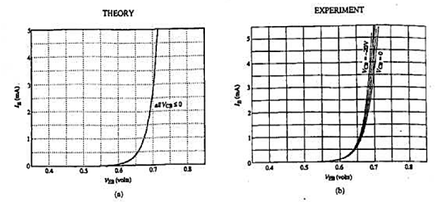
Input characteristics:
- From figure 15(a) and (b) it is clear that predicted and observed common-base input characteristics are same general character.
- The input current (IE) exponentially increases with increasing input voltage (VEB).
- The theoretically characteristics are essentially independent of the applied output voltage (VCB) but experimentally, however, the input current at a given input voltage noticeably increases with increasingly negative values of VCB.
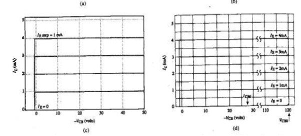
Output characteristics:
- Common base output characteristics are shown in Figures 15(c) and (d), there is a good agreement between theory and experiment.
- In both cases there is a rapid increase in the output current (IC) starting at slightly negative -VCB values, and a nearly perfect levelling-off or constancy of the output current for -VCB > 0.
- Theoretically there is no limit to the — VCB voltage that can be applied to the transistor. But for the real-device output voltage is limited to a maximum value of VCBO by some sort of breakdown phenomenon.
Figure 15 displays common-base input and output characteristics
|
Figure 15: Common base pnp BJT characteristics: (a) ideal theory and (b) experimental input characteristics; (c) ideal theory and (d) experimental output characteristics.
Common-Emitter Input and Output characteristics
Input characteristics:
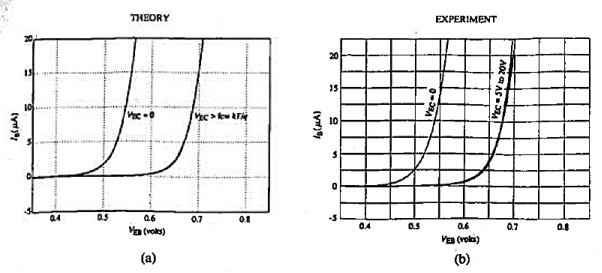
- From figure 16 (a) and (b) it is clear that predicted and observed common-emitter input characteristics are in good agreement for most of the part.
- For both VEC = 0 and VEC > few kT/q characteristic curve are in good agreements.
Output characteristics:
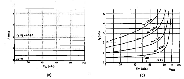
- The greatest deviation between theory and experiment can be found in the common emitter output characteristics shown in Figures 16(c) and (d).
- The theoretical characteristics are perfectly flat (VEC independent) under active mode biasing
- There is a very noticeable upward slope to the experimental curves even at relatively low output voltages.
- At large output voltages the experimental characteristics turn sharply upward.
- Finally some sort of breakdown phenomenon clearly limits the maximum low current output voltage, VCEO that can be applied to a transistor.
Overall the agreement between the ideal theory and experiment is surprisingly good. Deviations from the ideal that must be explained include the strong dependence of the common base input characteristics on the output voltage. The initial quasilinear slope and subsequent upward curvature of the common emitter output characteristics, and the VCBO and VCEO limitations imposed by breakdown phenomena.
|
Figure 16: Common emitter pnp BJT characteristics: (a) ideal theory and (b) experimental input characteristics; (c) ideal theory and (d) experimental output characteristics.
3.3.2 BASE WIDTH MODULATION
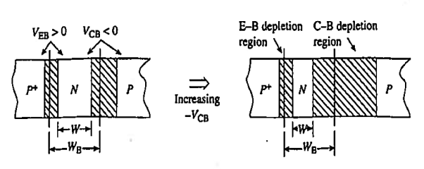
This phenomenon of the variation of W with the applied voltages is known as base width modulation or the Early effect.
While studying the characteristics curve we assume W = WB , we assumed that W is constant and independent of the applied voltages. But in reality the quasineutral width of the base is not a constant independent of the applied biases. Changing VEB and VCB, changes the depletion widths about the E—B or C—B junctions, thereby shrinking or expanding W as shown in figure.
|
Figure 17: Base width modulation Decrease in W resulting from an increase in the reverse bias applied across the C-B junction.
Note that even small variations in the depletion widths can be significant because of the narrow physical extent of the base.
Two of the deviations we studied before are direct results of this bias dependence.
Re-examining the equation used to generate the common base input characteristics, we can write
|
……… (1)
Assuming - VCB > few kT/q. Moreover, if one keeps only lowest-order terms in the W/LB <<1 expansion of the hyperbolic functions and neglects the typically small DEnEo/LE term, the defining equation for the common base input characteristics reduces to
 ………. (2)
Where the reverse bias applied to the C—B junction increases, the C—B depletion width increases and W decreases. IE at a given VEB is expected to increase with increasing -VCB. This is the result we obtain in the experimental characteristics shown in Figure 15(b).
Base width modulation is also responsible for the quasilinear increase in the common emitter output current recorded in figure 16(d).
Under active mode biasing common-emitter output characteristics reduces to
 ……….(3)
where  is given by
 ……….(4)
Since W decreases with increasing reverse bias across the C-B junction,  systematically increases with increasing VEC.
Thus, with base width modulation taken into account, the IC at a given IB under active mode biasing is likewise expected to increase with increasing VEC. It should be noted that base width modulation does not explain the sharp upturn in IC as the output voltage approaches VCE0.
Under active mode common base output characteristics is given by
 ………. (5)
where  is given by
 ………. (6)
In a well-made transistor the W-dependent terms in the denominator of the as expression are small compared to unity. As a result, even large changes in W give rise to an almost unnoticeable change in  . The ICB0 is W-independent and is moreover negligible in most instances.
Let us see the effect of transistor doping and the biasing mode on the sensitivity of base width modulation.
In a standard transistor NE >> NB >NC Thus almost all of the E-B depletion region lies in the base and most of the C-B depletion legion lies in the collector.
Under active mode biasing the E-B junction experiences only a small forward bias and plays a negligible role in modulating the quasineutral width of the base. The C-B junction is when subjected to a large reverse bias. The effect of base width modulation is minimized, however, because most of the C-B depletion region lies in the collector.
The opposite is true if the same transistor is operated in the inverted mode. In the inverted mode a reverse bias is applied across the E-B junction, the associated depletion width extends almost exclusively into the base, and the standard transistor is inherently quite sensitive to base width modulation.
3.3.3 PUNCH-THROUGH
Punch-through might be viewed as base width modulation carried to the extreme. Specifically, it refers to the physical situation where base width modulation has resulted in W  0.
0.
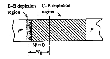
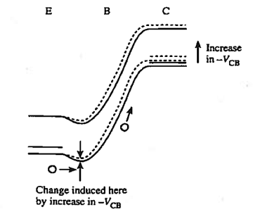
Punch through is the condition when the base is said to be punched through when the E-B and C-B depletion regions touch inside the base as shown in Figure 18(a)
|
Figure 18(a): Punch-through
|
Figure 18(b): Energy band diagram explanation of why a post punch through increase in the output voltage gives the to a large increase in the output (collector) current
Once punch-through has occurred, the E-B and C-B junctions become electrostatically coupled. As shown in Figure 18 an increase in -VCB beyond the punch-through point lowers the E-B potential hill and allows- a large (exponentially increasing) injection of carriers from the emitter directly into the collector. Only a slight increase in -VCB gives rise to a large increase in IC. If it occurs punch-through limits the maximum voltage (VCB0 or VCE0) that can be applied to a transistor. "if it occurs" leads to the another phenomena called Avalanche Multiplication.
3.3.4 AVALANCHE BREAKDOWN
Common Base
Let us consider BJT in common base configuration and active mode biased to a larger and larger - VCB, the carrier activity within the C-B depletion region of the BJT is very similar to that occurring in a simple pn junction diode. Number of the carriers increases and crossing the C-B depletion region. These carriers gain sufficient energy to create additional carriers by the impact ionization of semiconductor atoms. A point is eventually reached where a carrier avalanche occurs and the collector current increases rapidly toward infinity i.e. M , where M is the multiplication factor
Assuming avalanche breakdown takes place before punch-through, the maximum magnitude of the voltage that can be applied to the output of the BJT under common base operation, VCB0, is clearly just the breakdown voltage of the C-B junction.
Common Emitter
The common emitter case is far more interesting. The output voltage applied to a transistor connected in the common emitter configuration is
VEC = VEB - VCB
Under active mode biasing, the E-B junction is forward biased and VEB is typically quite small.
Thus for output voltages exceeding a few volts, we have
VEC = - VCB
From this it is to be expected that
VCE0  VCB0
VCB0
However, examining the experimental characteristics one finds a VCE0 considerably smaller than VCB0; VCE0  90V, whereas VCB0
 120V
120V
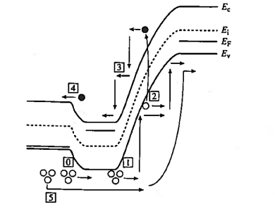
This unexpected result can be explained qualitatively with the help of Figure 19. The initial injection of holes into the base, labelled as  in the figure leads to the holes labelled as [1] entering the base-side of the C-B depletion region. Although the C-B junction is biased with voltage less than breakdown voltage, a few of these holes gain a sufficient amount of energy to impact ionize semiconductor atoms and create extra holes and electrons [2]. The added holes drift along with the injected holes into the collector; the added electrons are swept into the base labelled as [3] .
|
Figure 19: Step-by-step explanation of the carrier multiplication and feedback mechanism
The extra electrons in the base create a majority carrier imbalance that must be eliminated. The most efficient method of removing the excess would be for electrons to simply flow out of the base lead. This is precisely what happens when the BJT is connected in the common base configuration.
When the transistor is connected in the common emitter configuration, however, the base current is held constant during the measurement of the common emitter output characteristic—the extra electrons are not allowed to flow out the base lead. Consequently, the carrier imbalance in the base can only be alleviated by injecting electrons from the base into the emitter [4].
As was emphasized in the early operational discussion of the transistor, electron and hole injection across the E-B junction are intimately tied together. Every electron injected from the base into the emitter is accompanied by the injection of IEp/IEn added holes from the emitter into the base [5].
Thus for each additional electron-hole pair created in the C-B depletion region by impact ionization,
IEp/IEn +1 = 1/ (1- ) >
) >  dc +1 additional holes flow into the collector.
Effectively, the carrier multiplication in the C-B depletion region is internally amplified under common emitter operation. Moreover, the process we have just described is regenerative; i.e., it feeds back on itself. With added injection there is added carrier multiplication in the C-B depletion region and an even larger enhancement of the collector current. This all leads to an instability point where Ic  at a VEC far below the avalanche breakdown voltage of the C-B junction.
3.3.5 GEOMETRICAL EFFECTS
We have assumed the bipolar transistor to be "one-dimensional." with all currents primarily restricted to flowing in one direction.
It is obvious the current flow patterns must be decidedly more complex. This leads to several deviations from the ideal of a geometrical nature. Included under "geometrical effects" are internal voltage drops directly associated with the three-dimensional character of the current.
Emitter Area  Collector Area
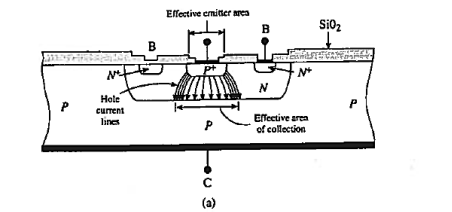
In the ideal model, carriers injected from the emitter into the base are assumed to travel in a straight line to the collector. The current flow path in an actual transistor can have a considerable lateral component. This is illustrated in Figure 20(a) using the cross section of a discrete planar transistor. The spread in current can be approximately taken into account by employing different effective areas for the emitter and collector.
Series Resistances
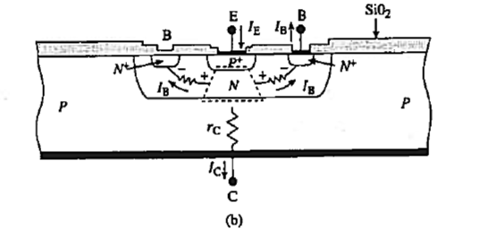
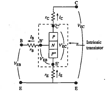
The base current flowing between the base contact and the "heart" of the transistor must pass through a resistive bulk region [the dashed line region in Figure 20(b). There is also a small resistance associated with the base contact itself. This means the voltage drop across the E—B junction is somewhat less than the VEB terminal voltage.
Although typically quite small in magnitude, the voltage difference is often significant because the E—B junction is forward biased under active mode operation and the emitter current is an exponential function of the junction voltage. To account for the voltage difference, one introduces a base series resistance, rB, equal to the sum of the bulk and contact resistances. If rB is the only series resistance of importance, then we used V’EB instead of VEB
V’EB = VEB - IBrB
|
Figure 20: Geometrical effects in a discrete planar transistor (a) Current spreading and crowding. (b) Base and collector series resistances. The dashed line region in (b) identifies the “intrinsic transistor,” the “heart” of the device.
As shown in Figure 21, individual series resistances connect the conceptual internal terminals of the intrinsic transistor to the external terminals of the physical transistor. In each case the series resistance is the sum of bulk and contact resistances. The voltages at the terminals of the intrinsic transistor are deduced from the applied voltages by accounting for the Ir drop across the relevant series resistance(s). The values of the series resistances are usually deduced from subsidiary measurements.
|
Figure 21: Series Resistances
Current Crowding
We have studied that the base current flows laterally from the heart of the transistor to the base contact. It also flows laterally across the face of the emitter, giving rise to a voltage drop in the base from the center to the edges of the emitter. The voltage applied across the E-B junction and the associated injection current from the emitter to the collector are therefore greatest at the edges of the emitter.
|
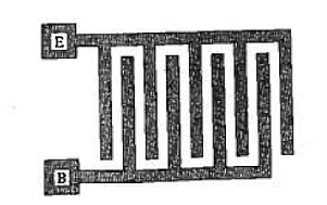
Figure 22: comb-like contact structure employed in power transistors to minimize current crowding.
A higher density of current lines was placed near the emitter edges in Figure 22 to illustrate the effect. This phenomenon, a larger current flow around the emitter periphery, is called current crowding.
Current crowding and the heating can become destructive at high current levels. To minimize the problem, power BJTs are constructed with emitters that have a large periphery-to-area ratio. This is achieved by connecting several narrow, long, emitter contacts into a comb-like structure and interdigitating the emitter contacts with base contacts as sketched in Figure 22.
3.3.6 R-G CURRENT
R-G current is known as Recombination—Generation Current. Thermal recombination-generation was assumed to be negligible throughout the E-B and C-B depletion regions in the ideal transistor analysis.
Under active mode operation with a small forward bias applied to the E-B junction, the R-G current from the E-B junction is likely to be the dominant component of the base current. This leads to a lower emitter efficiency and a reduced gain at low current levels (small VE).
Also, when the input is open circuited, the reverse-bias R-G current from the C-B junction adds to and is likely to dominate the observed output leakage current (ICB0 or ICE0).
The ideal transistor characteristics are not affected by the R-G current. Under most active-mode operating conditions, the input bias and current (IB or IE) are such that the diffusion component dominates the input current.
Moreover, at other than low input current levels, the output current extracted from the reverse-biased C-B junction is comprised primarily of the injected (diffusion dominated) current from the emitter.
Key Takeaways
- Deviations from the ideal that must be explained include the strong dependence of the common base input characteristics on the output voltage. The initial quasilinear slope and subsequent upward curvature of the common emitter output characteristics, and the VCBO and VCEO limitations imposed by breakdown phenomena.
- This phenomenon of the variation of W with the applied voltages is known as base width modulation or the Early effect.
- Punch through is the condition when the base is said to be punched through when the E-B and C-B depletion regions touch inside the base
- BJT in common base configuration and active mode biased to a larger and larger - VCB, the carrier activity within the C-B depletion region of the BJT is very similar to that occurring in a simple pn junction diode. The common emitter case is far more interesting.
- "geometrical effects" are internal voltage drops directly associated with the three-dimensional character of the current.
- To account for the voltage difference, one introduces a base series resistance, rB, equal to the sum of the bulk and contact resistances.
- The phenomenon, a larger current flow around the emitter periphery, is called current crowding.
- R-G current is known as Recombination—Generation Current. The ideal transistor characteristics are not affected by the R-G current.
The small-signal response is described or modelled in terms of a small-signal equivalent circuit. Small-signal equivalent circuits are employed, for example, to calculate amplifier signal gain, input impedances, and output impedances.
SMALL-SIGNAL EQUIVALENT CIRCUITS
3.4.1 Generalized Two-Port Model
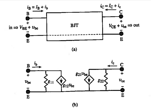
Consider BJT in the common emitter configuration and is modelled as a "black box" with two ports. Note that for the present analysis all currents are defined to be positive when flowing into a device terminal. Likewise, all voltages are referenced to the terminal common to the input and output.
With the BJT assumed to be connected in the common emitter configuration, the d.c. input current, the d.c. output current, the d.c. input voltage, and the d.c. output voltage are respectively IB, IC, VBE, and VCE. The corresponding a.c. quantities are ib, ic, vbe, and vce.
IB could be written as an exclusive function of the applied d.c. voltages; that is IB= IB(VBE, VCE).
When a.c. potentials vbe and vce, are superimposed on the d.c. terminal voltages, the input current quite generally becomes iB (VBE + vbe, VCE + vce) = IB(VBE, VCE)+ ib.
Similarly, it is readily established that the d.c. output current can also be expressed as an exclusive function of the d.c. input and output voltages; that is IC= IC(VBE, VCE). Thus When a.c. potentials vbe and vce are respectively added to VBE and VCE, the total output current analogously becomes iC (VBE + vbe, VCE + vce) = IC(VBE, VCE)+ ic.
|
Figure 23: (a) The BJT viewed as a two-port network and connected in the common emitter configuration. (b) Low-frequency small-signal equivalent circuit characterizing the a.c. response of the BE
Critical assumption; we assume the transistor can follow the changes in potential quasistatically so that is
or
|
Next, expanding the first term on the right-hand side of Eqs (3) and (4) in a Taylor series about the d.c. operating point, and keeping only first-order terms in the expansion (higher-order vbe and vce terms are assumed negligible) thus we obtain
When we substituted into equations (3) and (4)
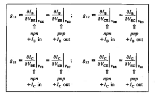
Dimensionally the partial derivatives in equations (7) and (8) are conductance. Introducing
This allows us to write
|
Equations (10) and (11) may be viewed as the a.c. current node equations for the base and collector terminals, respectively. These equations indicate the ib and ic, currents flowing into the terminals divide into two components.
One component (g11vbe at the input and g22vce at the output) is just the current through a conductance connected across the given port.
The second current component (g12vce at the input and g21vbe at the output) is controlled by the voltage at the opposite port and is logically associated with a current generator.
We therefore infer the small-signal circuit consistent with the derived equations is as pictured in Figure 23 (b). Some observation concerning the Figure 23 (b) result.
- The small-signal equivalent circuit is understood to be applicable at low operational frequencies where capacitive effects associated with the transistor junctions can be neglected.
- This system is practically less preferred as compared to Hybrid Model.
- The development leading is of a purely mathematical nature.
- The result could be readily modified to apply to other BJT configurations or even to other three-terminal devices by simply changing the identity of the two-port terminals.
- The only tie to a specific device or configuration is through the conductance definitions.
3.4.2 Hybrid-Pi Models
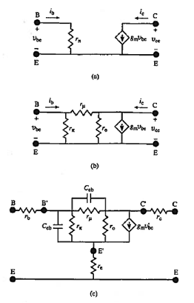
In performing small-signal analyses, the Hybrid-Pi equivalent circuit is by far and away the most frequently used model. The model has several advantages that make it particularly attractive to circuit design engineers. Notably, the model parameters are readily related to the d.c. operating point variables and the temperature variation of the parameters is easily deduced. Simplified and complete versions of the basic Hybrid-Pi model are shown respectively in Figure 24(a) and (b). The cited low-frequency equivalent circuits apply to the "intrinsic transistor" under active-mode operation. The Hybrid-Pi model gets its name from the Figure 24(b) π-arrangement of circuit elements with "hybrid" (a combination of conductance and resistance) units.
gm is the trans conductance, a measure of the forward voltage gain, ro, the output resistance, rπ the input resistance, and rμ is the feed through resistance. The simplified model of Figure 24 (a), which finds extensive use in first order analyses, can be derived directly from the generalized two-port model.
Under active-mode biasing for a pnp BJT
and
|
Figure 24: Hybrid-Pt equivalem circuits. (a) Simplified and (b) complete low-frequency Hybrid-Pi equivalent circuits that model the intrinsic transistor under active-mode coalman-emitter opera-tion. (c) High-frequency equivalent circuit including the parasitic series resistances.
If base-width modulation is assumed to be negligibk,  F and IF0 constants independent of bias and
 …………… (4)
and
 …………… (5)
With g11 = g22 = 0 we obtain the desired result. We also conclude gm  g21, and rπ= 1/ g11. Thus gm and rπ is given by
 …………… (6)
 …………… (7)
gm and rπ can be calculated using operating point. The four-element low-frequency model of Figure 24(b) is used when base-width modulation cannot be ignored or a more precise analysis is to be performed.
Circuit parameters can be related to the two-port model parameters in a straightforward fashion.
 …………… (8)
 …………… (9)
 …………… (10)
 …………… (11)
Typically g12 is small and may be neglected in computing gm ro and rπ. Equations (6), (7) can be used to evaluate gm and rπ if g12 is much less than g21 and g11.
Finally, the model shown in Figure 24(c) is appropriate for use at higher frequencies. Included in the model are the parasitic series resistances (rb, re, rc) that connect the intrinsic transistor to the external device terminals.
Ccb and Cbe respectively model the collector-base and emitter-base pn junction capacitances.
It should be noted that the Figure 24(c) model is typically valid at frequencies up to roughly 500 MHz. The model becomes increasingly inaccurate above 500 MHz because it does not take into account the delays in signal propagation across the various device regions.
Key Takeaways
- The small-signal response is described or modelled in terms of a small-signal equivalent circuit.
- Small-signal equivalent circuits are employed, for example, to calculate amplifier signal gain, input impedances, and output impedances.
- Generalized Two-Port Model and Hybrid-Pi Models used for this purpose
- BJT in the common emitter configuration and is modelled as a "black box" with two ports
- Generalized Two-Port Model is practically less preferred as compared to Hybrid Model.
- Hybrid-Pi model has several advantages that make it particularly attractive to circuit design engineers. Notably, the model parameters are readily related to the d.c. operating point variables and the temperature variation of the parameters is easily deduced.
Reference Books
- Principle of electronics S. Chand V K Mehta and Rohit Mehta
- Semiconductor Device Fundamentals by Robert F. Pierret

