Unit 2
Characteristics of OP-AMP
- The open loop voltage gain is infinity.
- The input impedance is infinity.
- Output impedance is zero.
- The bandwidth is infinity
- The output voltage is zero when both inputs are equal. That is zero offset voltage.
- Infinite CMRR
- Slew rate is infinite
- Power supply rejection ratio is zero
- They do not drift with temperature.
The current taken from the source into the op-amp inputs respond differently to current and voltage due to mismatch in transistor.
DC output voltages are,
1. Input bias current
2. Input offset current
3. Input offset voltage
4. Thermal drift
1. Input bias current:
The input to op-amp is differential amplifierwhich is made of BJT or FET.
In an ideal op-amp no current is drawn from the input terminal on assumption.
The base currents enterinto the inverting and non-inverting terminals (IB-& IB+ respectively).
Even though both the transistors are identical, IB- and IB+ are not exactly equal due to internal imbalance between the two inputs.
· Manufacturers specify the input bias current IB
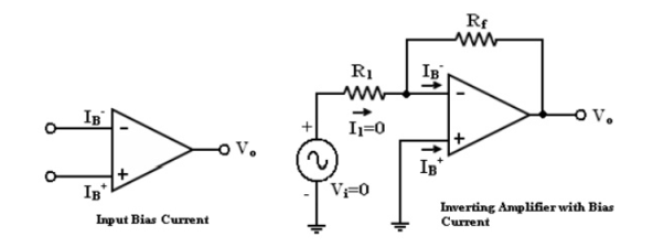
If input voltage Vi=0V then the output voltage Vo should also be (Vo = 0) IB = 500nA.
We find the output voltage is offset by
Vo = IB . Rf
Op-amp with a 1M feedback resistor
V0 = 5000nA X 1M = 500mV
The output is driven to 500mV with zero input, because of the bias currents.
In application where the signal levels are measured in mV, this is totally unacceptable. This can be compensated by resistor Rcomp which is added between the non-inverting input terminal and ground as shown in the figure below.
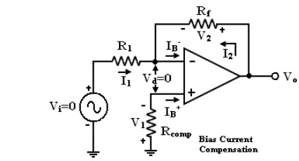
Current IB+ flowing through the compensating resistor Rcomp, then by KVL we
-V1+0+V2-Vo = 0 (or)
Vo = V2 – V1 ——>(3)
By selecting proper value of Rcomp, V2 can be cancelled with V1 and Vo = 0.
The value of Rcomp is derived as
V1 =I=+Rcomp (or)
IB+ = V1/Rcomp ——>(4)
The node =a‘is at voltage (-V1). Because the voltage at the non-inverting input terminal is (-V1). So, with Vi = 0 we get,
I1 = V1/R1 ——>(5)
I2 = V2/Rf ——>(6)
For compensation, Vo should equal to zero (Vo = 0, Vi = 0). i.e. from equation (3) V2 = V1. So that,
I2 = V1/Rf ——>(7)
KCL at node =a‘ gives,
IB-= I2 + I1
IB- = RfR1
Assume IB- = IB+ and using equation (4) & (8) we get
Rcomp = R1 + Rf
Rcomp = R1 || Rf --->(9)
To compensate for bias current, the compensating resistor, Rcomp combination of resistor R1 and Rf.
2. Input offset current:
Bias current compensation works if both bias currents IB+ and IB- are equal.
Since the input transistor cannot be made identical. There will always be some small difference between IB+ and IB-. This difference is called offset current
|Ios| = IB+ -IB- -----(10)
The Offset current Ios for BJT op-amp is 200nA and for FET op-amp is 10pA.
Even with bias current compensation, offset current will produce an output voltage when Vi = 0.
V1 = IB + R comp ---------------------(11)
I1 = V1 / R1 -------------------------------(12)
KCL at node = ‘a’ gives
Vo = I2 Rf – V1
Vo = I2 Rf – IB +Rcomp
Vo = 1 M Ω x 200 n A
Vo = 200mV with Vi=0.
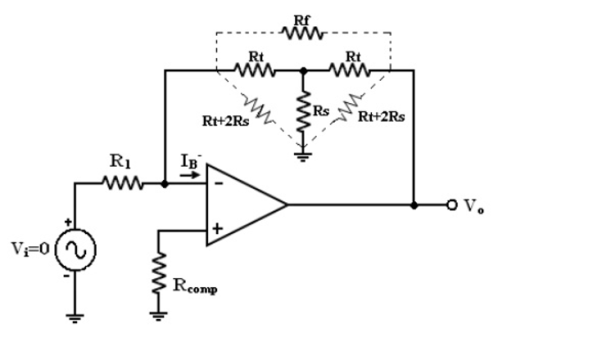
To obtain high input impedance, R1 must be kept large. If R1 is large the feedback
The T-feedback network is a good solution. This will allow large feedback resistance, while keeping the resistance to ground low (in dotted line).
The T-network provides a feedback signal as if the network were a single feedback resistor.
By T to Π conversion,
To design T- network first pick Rt<<Rf/2
Then calculate Rs = Rf 2 Rt
3. Input offset voltage:
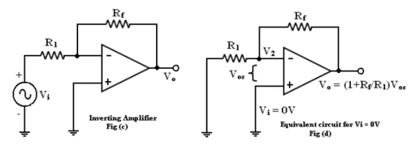
Though compensating technique have been used the output voltage may still not be zero with zero input voltage [Vo ≠ 0 with Vi = 0]. This is due to unavoidable imbalances inside the op-amp and one may have to apply a small voltage at the input terminal to make output (Vo) = 0.
This voltage is called input offset voltage Vos. This is the voltage required to be applied at the input for making output voltage to zero (Vo = 0).
Total output offset voltage:
The total output offset voltage VOTcan be either more or less than the offset voltage produced at the output due to input bias current (IB) or input offset voltage because IB and Vos could be either positive or negative with respect to ground.
Therefore, the maximum offset voltage at the output of an inverting and non-inverting amplifier (figure b, c) without any compensation technique used is given by many op-amp provide offset compensation pins to nullify the offset voltage.
4. Thermal drift:
Bias current, offset current, and offset voltage change with temperature.
A circuit carefully nulled at 25ºC may not remain. So, when the temperature rises to 35ºC. This is called drift.
Offset current drift is expressed in nA/ºC.
These indicate the change in offset for each degree Celsius change in temperature.
Frequency Response:
The variation in operating frequency causes variations in gain magnitude and its phase angle. The way the gain of the op-amp responds to different frequencies is called the frequency response.
For an op-amp with only one break (corner) frequency all the capacitors effects can be represented by a single capacitor C. The below figure represents the modified variation of the low frequency model with capacitor C at the output.
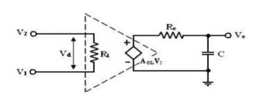
There is one pole due to R0C and one -20dB/decade. The open loop voltage gain of an op-amp with only one corner frequency is obtained from the above fig.
f1 is the corner frequency or the upper 3 dB frequency of the op-amp.
The magnitude and phase angle characteristics:
1. For frequency f<< f1 the magnitude of the gain is 20 log AOL in db.
2. At frequency f = f1 the gain in 3 dB down from the dc value of AOL in db. This frequency f1 is called corner frequency.
3. For f>> f1 the fain roll-off at the rate off -20dB/decade or -6dB/decade.
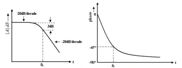
Frequency response of op-amp
From the phase characteristics that the phase angle is zero at frequency f = 0. At the corner frequency f1 the phase angle is -45º
 (lagging and an infinite frequency the phase angle is -90
 . It shows that a maximum of 90
 phase change can occur in an op-amp with a single capacitor C. Zero frequency is taken as the decade below the corner frequency and infinite frequency is one decade above the corner frequency.
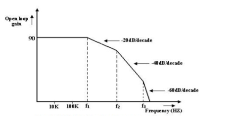
Roll off rate of op-amp gain
A circuit or a group of circuit connected as a system is said to be stable, if its o/p reaches a fixed value in a finite time. A system is said to be unstable if its o/p increases with time instead of achieving a fixed value.
Bode plots are compared of magnitude Vs Frequency and phase angle Vs frequency.
Any system whose stability is to be determined can represented by the block diagram.
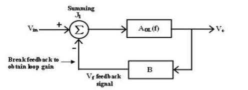
The block between the output and input is referred as forward block and the block between the output signal and f/b signal is referred to as feedback block.
The content of each block is referred as transfer frequency.
From fig. We represented it by AOL (f) which is given by
AOL (f) = V0/Vin if Vf = 0 ----- (1)
Where AOL (f) = open loop volt gain.
The closed loop gain Af is given by AF = V0/Vin
= AOL / (1+(AOL ) (B) ----(2)
B = gain of feedback circuit.
B is a constant if the feedback circuit uses only resistive components.
Once the magnitude Vs frequency and phase angle Vs frequency plots are drawn, system stability may be determined as follows
1. Method 1:
Determine the phase angle when the magnitude of (AOL) (B) is 0dB (or) 1.
If phase angle is >-180 , the system is stable. However in some systems the magnitude may never be 0 hence method 2 is used.
2. Method 2:
Determine the phase angle when the magnitude of (AOL) (B) is 0dB (or) 1.
If phase angle is > - 180 If the magnitude is negative decibels, then the system is stable. However, in some systems the phase angle of a system may reach -1800, under such conditions method 1 must be used to determine the system stability.
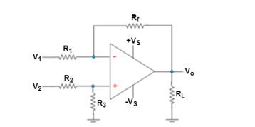
Differential Amplifier using Op-amp
Here V1 and V2 represent the voltages applied at its inverting and non-inverting input terminals and Ad refers to its differential gain.
The output of the differential amplifier is given as
Vo = Ad (V1 – V2) + Ac (V1 + V2/2)
where AC is called the common mode gain of the amplifier.
Hence its output voltage will be equal to the sum of the output voltages produced by the Op-Amp circuit operating as an inverting amplifier and the Op-Amp circuit operating as a non-inverting amplifier.
Thus, one gets,
Vo = -Rf/R1 V1 + V2. Rf / R2 + R3 (1 + Rf/R1)
Now, if R1 = R2 and R3 = Rf, then
Vo = -Rf/R1 V1 + V2 . Rf/ R1 + Rf ( R1 + Rf/R1)
Vo = - Rf/R1 . V1 + V2 . Rf /R1
Vo = - Rf/R1 (V1 – V2)
This implies that the gain of the differential amplifier circuit is given by -Rf/R1.
In open loop configuration the gain of op-amp is not constant and varies with frequency and the product of gain and frequency remains constant till the unity gain frequency for op-amp known as gain bandwidth product of op-amp.
Gain bandwidth product is the bandwidth of op-amp when voltage gain is 1.
Ideally infinite bandwidth
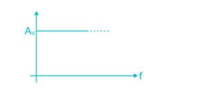
This means ideally op-amp amplifies all the frequency with equal gain. But ideally gain depends on frequency. Gain depends on frequency because of capacitive components present due to:
- Junction capacitance of FET and BJT at high frequencies
- Construction of op-amp using FET and MOSFET which forms MOS capacitance.
Interconnects are used to connect different stages. These capacitances limits the maximum frequency of op-amp which is given by slew rate. To model all these capacitances in ideal model capacitor is connected at the output.
Inverting Amplifier
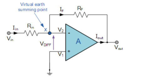
The input signal vi is applied to the inverting input terminal through resistor R1 and non-inverting input terminal is grounded. The feedback from the output of the inverting terminal is provided through the feedback resistor Rf.
Since the input is applied to the inverting terminal vo and vi are opposite in polarity and hence the feedback is negative. Since the non-inverting input terminal is grounded v2=0. Due to virtual short at the input of op-amp the inverting and non-inverting input terminals are at the same potential.
Therefore, v1 = v2 = 0.
Due to high input impedance of Op-amp the current flowing into its inverting input terminal is zero. Therefore, the same current flows through R1 and Rf .
i 1 = i f
But i1 = vi – v1 / R1 = vi/R1
i f = v1 – vo / Rf = -vo/Rf
Vi/R1 = - vo/Rf
Af = vo/vi = -Rf/R1
Af is the closed loop voltage gain or voltage gain with negative feedback.
Problem:
A 200mV peak to peak sine waveform voltage is applied to Op-amp inverting amplifier with Rf/R1 = 10.
Solution:
Peak to peak input voltage
2Vm = 200 mV
Vm = 100 mV
Vi= Vm sin wt = 100 sin wt mV
Vo = -Rf/R1 x vi = -10 x 100 sinwt mV
= -1000 sin wt mV
Non-inverting amplifier
Non- Inverting amplifier is one in which the output is in phase with respect to input that is if you apply a positive voltage, output will be positive. The output is an non -inverted amplified version of input.
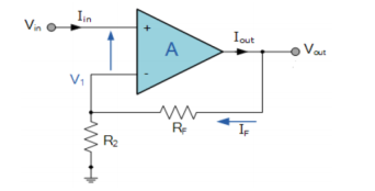
Assuming the op-amp is ideal and applying the concept of virtual short, the voltage at the inverting terminal is equal to non- inverting terminal.
Applying KCL at inverting node we get
Vi -Vo/ R2 + Vo – 0 / R1 = 0
By rearranging the terms, we will get
Voltage gain Av = Vo/ Vi = (1+ Rf/Ri)
Gain of non- inverting amplifier Av= (1+ Rf/Ri).
Problem
Design a non-inverting amplifier using Op-amp with a closed loop voltage gain of 10.
Solution:
Af = 1 + Rf/R1 =10
Rf/R1 = 9
Rf = 9 R1
If R1 = 1K
Rf = 9K Ω
In an op-amp inverting amplifier R1 = 1K Ω and Rf = 100KΩ. The DC supply voltage of the op-amp is ± 15V. Calculate the output voltage if input voltage is 1V.
R1 = 1KΩ Rf = 100KΩ
V+ = 15V and V-=-15V. Vi = 1V
Af = -Rf/R1 = -100K/1K = -100
Af = vo/vi
Vo = Af vi
= -100 x 1V = -100V
The output voltage cannot exceed the DC power supply voltage . Since vo is negative and large it is limited to V-
Vo ≈ V- = -15V
A voltage to current converter or V to I converter, is a circuit that takes current as the input and produces voltage at the output.
An op-amp based voltage to current converter produces an output current when a voltage is applied to its non-inverting terminal. The circuit diagram of an op-amp based voltage to current converter is shown in the following figure.
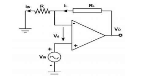
The input voltage Vi is applied at the non-inverting input terminal of the op-amp. According to the virtual short concept, the voltage at the inverting input terminal of an op-amp will be equal to the voltage at its non-inverting input terminal. So, the voltage at the inverting input terminal of the op-amp will be Vi.
The nodal equation at the inverting input terminal's node is −
ViR1−I0=0
=>I0=VtR1
Thus, the output current I0 of a voltage to current converter is the ratio of its input voltage Vi and resistance R1.
We can re-write the above equation as −
I0Vi=R1
The above equation represents the ratio of the output current I0 and the input voltage Vi & it is equal to the reciprocal of resistance R1.
The ratio of the output current I0 and the input voltage Vi is called as Transconductance.
The ratio of the output and the input of a circuit is called as gain. So, the gain of an voltage to current converter is Transconductance and it is equal to the reciprocal of resistance R1.
Current to Voltage Converter
A current to voltage converter or I to V converter is the circuit that takes current as the input and produces voltage as the output.
An op-amp based current to voltage converter produces an output voltage when current is applied to its inverting terminal. The circuit diagram of an op-amp based current to voltage converter is shown in the following figure.
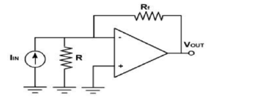
In the circuit shown above, the non-inverting input terminal of the op-amp is connected to ground. That means zero volts is applied at its non-inverting input terminal.
According to the virtual short concept, the voltage at the inverting input terminal of an op-amp will be equal to the voltage at its non-inverting input terminal. So, the voltage at the inverting input terminal of the op-amp will be zero volts.
The nodal equation at the inverting terminal's node is −
−Ii+0−V0Rf=0
−Ii=V0Rf
V0=−RtIi
Thus, the output voltage, V0 of current to voltage converter is the negative product of the feedback resistance, Rf and the input current, It. Observe that the output voltage, V0 is having a negative sign, which indicates that there exists a 1800 phase difference between the input current and output voltage.
The above equation as −
V0Ii=−Rf
The above equation represents the ratio of the output voltage V0 and the input current Ii, and it is equal to the negative of feedback resistance, Rf. The ratio of output voltage V0 and input current Ii is called as Trans resistance.
As the input impedance of op-amp is too large hence more than one input signal can be applied to the inverting terminal or non-inverting terminal of Op-amp. The output of this circuit is addition of two input signals. Hence it is called adder or summer circuit.
Inverting summer of adder
If two or more input signals are applied to the inverting terminal of op-amp the output is the sum of these inputs called as inverting summer.
Pg (246)
Consider the following figure . Let V1 and V2 be the input voltages applied to the inverting input of an op-amp through R1 and R2 as shown in figure.
The feedback resistor Rf connected between output of inverting input of op-amp and non-inverting input terminal is grounded. Applying KCL at node A we get
i 1 + i 2 = if + ib ------------------------------------------(1)
Here ib =0 because ideal op-amp has infinite input impedance therefore it draws zero current
i 1 + i 2 = i f ---------------------------------------------------------(2)
Applying ohms law to find currents i1 , i2 and if we get
V1 – VA / R1 + V2 – VA / R2 = VA – Vo / Rf ----------------------------(3)
According to virtual ground concept VB = VA = 0
V1/ R1 + V2 / R2 = -Vo/ Rf ----------------------------------------------------------------(4)
Vo = -Rf ( V1 / R1 + V2 / R2) -----------------------------------------------(5)
Substitute R1 = R2 = Rf = R in equation (5) we get
Vo = -R/R (V1+V2) ---------------------------------------------------------(6)
Vo = -(V1+V2) ----------------------------------------------------(7)
Therefore, the output of op-amp is equal to the sum of input voltages. The negative sign indicates that the output voltage is 180 0 out of phase with respect to input voltage.
Non – inverting Summer
Let V1 and V2 be the input voltages applied to the non-inverting input of op-amp through R1 and R2 as shown in figure.
Pg (247)
Let V1 and V2 be the input voltages applied to the non-inverting input of op-amp through R1 and R2 as shown in figure.
Figure 5.15
The feedback resistor Rf connected between output to inverting input of op-amp and the inverting input terminal through R is grounded. Now by applying KCL at node B we get
i 1 + i 2 = ib ------------------------------------(1)
But here ib =0 because ideal op-amp has an infinite input impedance and hence draws zero current
i1 + i 2 =0 -----------------------------------------(2)
Applying Ohms law to find currents i1 and i2 we get
V1 -VB / R1 + V2 – VB/ R2 =0 -----------------------------------(3)
V1/ R1 + V2 / R2 = VB( 1/R1 + 1/R2 )----------------------------------------(4)
VB = (V1/ R1 + V2 / R2) / ( 1/R1 + 1/R2 )
VB = V1 R2 + V2 R1 / R2 + R1 -------------------------------------------------(5)
Apply KCL at node A we get
If=i-------------------------------------------------------------------(6)
Applying Ohms law to find current if and i we get
Vo – VA / Rf = VA / R ---------------------------------------------------(7)
Vo/Rf = VA( 1/R + 1/ Rf) ---------------------------------------(8)
Vo = VA ( 1 + Rf/R) --------------------------------------------------------------(9)
According to virtual ground concept substituting VB = VA in equation (9) we get
Vo = VB(1+Rf/R)
Vo = VB(R+Rf/R)--------------------------------------------------(10)
Substitute eq(5) in (9) we get
Vo = (R + Rf/R) (V1R2 + V2 R1 / R1 + R2)--------------------------------(11)
Let us assume R1 =R2=Rf=R in eq(11) we get
Vo = (R+R/R)(V1R + V2 R / R + R )
Vo = (V1 + V2)
Therefore, the output voltage of non-inverting summer is equal to the sum of two input voltages.
In differentiator circuit the output voltage is the differentiation of input signal. The differentiator circuit consists of passive elements R,L,C called passive differentiator.
Consider the op-amp differentiator as shown in figure.
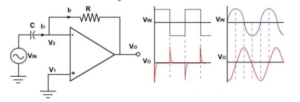
Apply KCL to node A, we get
Ic = if + ib
Here ib=0 because ideal op-amp has infinite input impedance and hence draws zero current.
Applying Ohms law find current ic and if we get
C dVc/dt = VA – Vo / Rf
Since Vc is the voltage across capacitor
C d(Vin – VA)/ dt = VA – Vo / Rf
According to virtual ground concept VA = VB =0
Therefore,
C dVin /dt = -Vo/Rf
Vo = -1/Rf C d/dt . Vin
From the above equation it is clear that the output voltage is proportional to the differentiation of input voltage Vin. The product Rf C is the time constant of the differentiator.
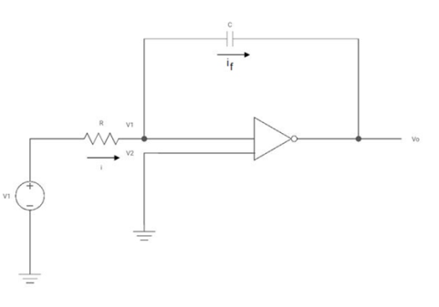
Since the non-inverting input terminal of op-amp is grounded v2=0. Due to virtual short at the input of op-amp the inverting and non-inverting input terminals are at the same potential
Therefore v1=v2=0
Due to high impedance of op-amp the current flowing into its input terminal is zero. Therefore the same current flows through R and C
That is
i1 = if -------------------(1)
Where i1 = vi – v1 /R= vi -/R---------------------(2)
And if = C d/dt[v1 – v0] = -C dv0/dt --------------------(3)
Substituting (2) and (3) in (1) we get
Vi = - C/R dv0/dt ------------------------(4)
Dvo/dt = (-1/RC) vi ---------------------------- (5)
Integrating both sides of eq(5) we get
v0 = - 1/RC  + v0(0) --------------------------(6)
Where v0(0) is the initial voltage on the capacitor at t=0.
Note: v0(o) represents the constant of integration.
From eq(6) we find that the output voltage is proportional to the integral of the input voltage.
Therefore v0 = - 1/RC 
Problem:
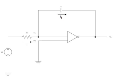
The integrator circuit as shown in the figure has R = 500K Ω and C=1µF. Find and plot the output voltage for the inputs as shown in the figure.
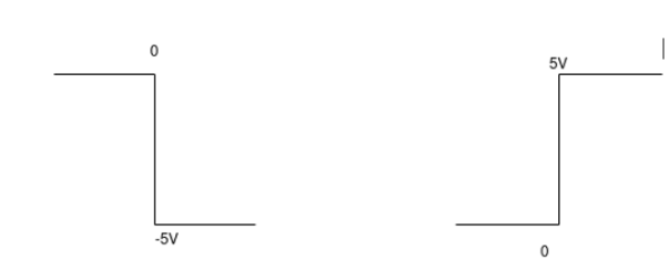
a) vi =- 5V b) When vi=5V
c)vi= 2 sin 4tV d) vi= 4tV
Solution:
We know that
v0 = - 1/RC  + v0(0)
Here R= 500K Ω and C = 1µF
1/RC = 1/ 500 x 1000 x 1 x 10-6
= 1/RC = 2
When vi=-5V
= -2  ; vi =- 5V
= -2 
= 10t V
Which means it is a ramp voltage with positive slope.
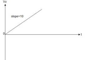
When vi=5V
-2  ; vi = 5V
= -2 
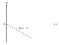
= -10t V
Which means it is a ramp voltage with negative slope.
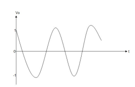
When vi= 2 sin4t V
Vo = -2 
= -4 [-cos 4t] /4
= cos 4t
When vi=4t V
Vo = 
= -8 [t2/2]
= - 4V

References:
Basic Electronics (VTU) by Professor D Chattopadhyay , Professor P C Rakshit, New Age International (P) Ltd., Publishers
Basic Electronics ByTheraja B.L.
CIRCUIT FUNDAMENTALS and BASIC ELECTRONICS Ashish Chaudhury and R. K. Verma.
Basic Electronics by D P Kothari, I J Nagrath