Unit 3
Applications of OP AMP
The Instrumentation amplifiers consist of three op-amps. In this circuit, a non-inverting amplifier is connected to each input of the differential amplifier.
This instrumentation amplifier provides high input impedance for exact measurement of input data from transducers. The circuit diagram of an instrumentation amplifier is as shown in the figure below.
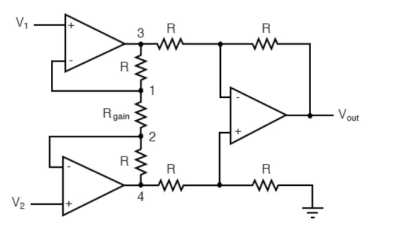
The op-amps 1 & 2 are non-inverting amplifiers and together form an input stage of the instrumentation amplifier. The op-amp 3 is a difference amplifier that forms the output stage of the instrumentation amplifier.
Working
The output stage of the instrumentation amplifier is a difference amplifier, whose output Vout is the amplified difference of the input signals applied to its input terminals.
If the outputs of op-amp 1 and op-amp 2 are Vo1 and Vo2 respectively, then the output of the difference amplifier is given by,
Vout = (R3/R2)(Vo1-Vo2)
The expressions for Vo1 and Vo2 can be found in terms of the input voltages and resistances.
Consider the input stage of the instrumentation amplifier as shown in the figure below.
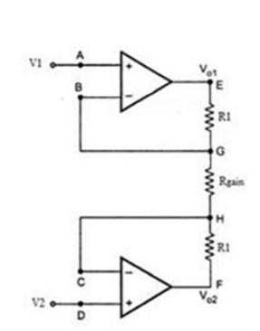
The potential at node A is the input voltage V1. Hence the potential at node B is also V1, from the virtual short concept. Thus, the potential at node G is also V1.
The potential at node D is the input voltage V2. Hence the potential at node C is also V2, from the virtual short. Thus, the potential at node H is also V2.
Ideally the current to the input stage op-amps is zero. Therefore, the current I through the resistors R1, Rgain and R1 remains the same.
Applying Ohm’s law between the nodes E and F,
I = (Vo1-Vo2)/(R1+Rgain+R1) ——————— 1
I = (Vo1-Vo2)/(2R1+Rgain)
Since no current is flowing to the input of the op-amps 1 & 2, the current I between the nodes G and H can be given as,
I = (VG-VH)/Rgain = (V1-V2)/Rgain ————————- 2
Equating equations 1 and 2,
(Vo1-Vo2)/(2R1+Rgain) = (V1-V2)/Rgain
(Vo1-Vo2) = (2R1+Rgain)(V1-V2)/Rgain —————— 3
The output of the difference amplifier is given as,
Vout = (R3/R2) (Vo1-Vo2)
Therefore, (Vo1 – Vo2) = (R2/R3)Vout
Substituting (Vo1 – Vo2) value in the equation 3, we get
(R2/R3)Vout = (2R1+Rgain)(V1-V2)/Rgain
i.e. Vout = (R3/R2){(2R1+Rgain)/Rgain}(V1-V2)
The above equation gives the output voltage of an instrumentation amplifier. The overall gain of the amplifier is given by the term (R3/R2){(2R1+Rgain)/Rgain}.
Advantages
The gain of a three op-amp instrumentation amplifier circuit can be easily varied and controlled by adjusting the value of Rgain without changing the circuit structure.
The gain of the amplifier depends only on the external resistors used. Hence, it is easy to set the gain accurately by choosing the resistor values carefully.
The input impedance of the instrumentation amplifier is dependent on the non-inverting amplifier circuits in the input stage. The input impedance of a non-inverting amplifier is too high.
The output impedance of the instrumentation amplifier is the output impedance of the difference amplifier, which is too low.
The CMRR of the op-amp 3 is high and almost all of the common mode signal will be rejected.
A logarithmic amplifier, or a log amplifier, is an electronic circuit that produces an output that is proportional to the logarithm of the applied input.
An op-amp based logarithmic amplifier produces a voltage at the output which is proportional to the logarithm of the applied voltage applied to the resistor connected to its inverting terminal.
The circuit diagram of an op-amp based logarithmic amplifier is shown below−
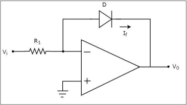
In the above circuit, the non-inverting input terminal of the op-amp is connected to ground which means zero volts is applied at the non-inverting input terminal of the op-amp.
In virtual short concept, the voltage at the inverting input terminal of an op-amp will be equal to the voltage at its non-inverting input terminal. So, the voltage at the inverting input terminal will be zero volts.
The nodal equation at the inverting input terminal’s node is −
0−Vi/R1+If=0
If = Vi/R1 -------------------------(1)
The equation for current flowing through a diode, when it is in forward bias
If=Ise(Vf/nVT)--------------------------(2)
Where,
Is - the saturation current of the diode,
Vf - the voltage drops across diode, when it is in forward bias,
VT - the diode’s thermal equivalent voltage.
The KVL equation around the feedback loop of the op amp will be −
0−Vf−V0=0
=>Vf=−V0
Substituting the value of Vf in Equation 2, we get −
If=Ise(−V0/nVT)…………………........(3)
The left- hand side terms of both equation 1 and equation 3 are same. Hence, equating the right- hand side term we get
Vi/R1=Ise(−V0/nVT)
Vi/R1Is=e(−V0/nVT)
Applying logarithm on both sides, we get −
In(Vi/R1Is)=−V0/nVT
V0=−nVTIn(Vi/R1Is)
Note that in the above equation, the parameters n, VT and Is are constants. So, the output voltage V0 will be proportional to logarithm of the input voltage Vi for a fixed value of resistance R1.
The output voltage V0 has a negative sign, which indicates that there exists a 1800 phase difference between the input and the output.
Anti-Logarithmic Amplifier
The anti-log amplifier is an electronic circuit which produces an output that is proportional to anti-logarithm of the applied input.
The circuit diagram of an op-amp based anti-logarithmic amplifier is shown in the following figure −
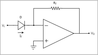
From the figure the non-inverting input terminal of the op-amp is connected to ground. It means zero volts is applied to its non-inverting input terminal.
In virtual short concept, the voltage at the inverting input terminal of op-amp will be equal to the voltage present at its non-inverting input terminal.
So, the voltage at its inverting input terminal will be zero volts.
The nodal equation at the inverting input terminal’s node is −
−If+0−V0Rf=0
=>−V0/Rf=If
=>V0=−Rf x If.......Equation4
The equation for the current flowing through a diode, when it is in forward bias, is as given below −
If=Ise(Vf/nVT)
Substituting the value of Ifin Equation 4, we get
V0=−Rf{Ise(Vf/nVT)}
V0=−RfIse(Vf/nVT)......Equation5
The KVL equation at the input side of the inverting terminal of the op amp will be
Vi−Vf=0
Vf=Vi
Substituting, the value of 𝑉𝑓 in the Equation 5, we get −
V0=−Rf { Ise(Vi/nVT)
Note that, in the above equation the parameters n, VT and Is are constants. So, the output voltage V0 will be proportional to anti-natural logarithm (exponential) of the input voltage Vi, for a fixed value of feedback resistance Rf.
The output voltage V0 is having a negative sign, which indicates that there exists 1800 phase difference between the input and the output.
FIRST-ORDER LOW-PASSBUTTER WORTH FILTER
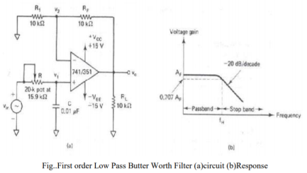
Fig. Shows a first-order low-pass Butterworth filter that uses an RC network for filtering.
Note that the op- amp is used in the non-inverting configuration; hence it does not load down the RC network.
ResistorsR1 and RF determine the gain of the filter. According to the voltage-divider rule, the voltage at the non- inverting terminal (across capacitor C)is
V1 = -jXc/ R-jXc . Vin
j=√-1 and -jXc = 1/j2π f C
V1 = Vin / 1+j 2 π f RC
Vo = 1 + RF/ R1 V1
Vo = (1 + Rf/R1) . Vin / 1+j 2 π f RC
Vo/Vin = AF/ 1 + j (f/fH)--------------------------------(1)
Where Vo/Vin = gain of the filter as a function of frequency
AF = (1+Rf/R1) = pass band gain of the filter
F= input frequency of the filter
FH = 1/ 2 π RC = upper cut-off frequency of the filter
The gain and phase angle equations of low pass filter can be obtained by converting Equation (1) into its equivalent polar form as follows:
|Vo|/ |Vin|= AF/ √ 1 + (f/fH) 2
ɸ = tan-1 (f/fH)
Where ɸ is the phase angle in degrees
SECOND-ORDER LOW-PASSBUTTER WORTH FILTER
A stop-band response having a 40-dB/decade roll-off is obtained with the second order low- pass filter. A first-order low-pass filter can be converted into a second order type simply by using an additional RC network, as shown in Figure
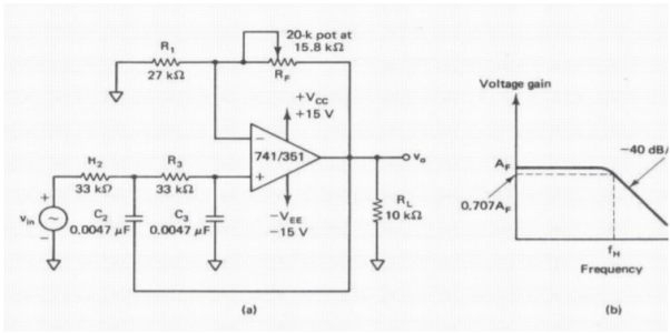
Second-order filters are important because higher-order filters can be designed using them. The gain of the second-order filter is set by R1 and RF, while the high cutoff frequency fH is determined by R2, C2, R3, and C3, as follows
FH = 1/ 2 π √ R2 R3 C2 C3
The voltage gain is given by
|Vo|/ |Vin|= AF/ √ 1 + (f/fH) 2
Pass band gain of the filter is given by
Af = (1 + Rf/R1) = pass band gain of the filter.
A comparator compares a signal voltage on one input of an op-amp with a known voltage called a reference voltage on the other input. Comparators are used in Digital Interfacing Schmitt Trigger Discriminator Voltage level detector and oscillators.
Non-inverting Comparator:
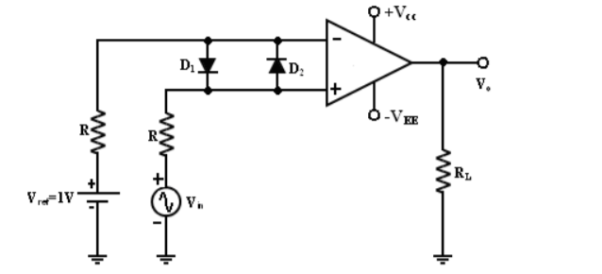
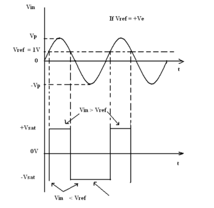
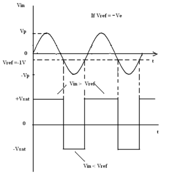
A fixed reference voltage Vref of 1 V is applied to the negative terminal and time varying signal voltage Vin is applied to the positive terminal.
When Vin is less than Vref the output becomes V0 at –Vsat [Vin <Vref => V0 (-Vsat)].
When Vin is greater than Vref, the (+) input becomes positive, the V0 goes to +Vsat. [Vin >Vref=> V0 (+Vsat)].
Thus, V0 changes from one saturation level to another.
The diodes D1 and D2 are used to protect the op-amp from damage due to the excessive input voltage Vin. Because of these diodes, the difference input voltage Vid of the op-amp diodes are called clamp diodes. The resistance R in series with Vin is used to limit the current through D1 and D2.
To reduce offset problems, a resistance Rcomp = R is connected between the negative input and Vref.
Inverting Comparator
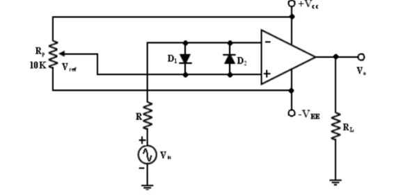
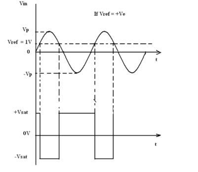
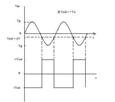
This fig shows an inverting comparator in which the reference voltage Vref is applied to the (+) input terminal and Vin is applied to the (-) input terminal.
In this circuit Vref is obtained by using a 10K potentiometer that forms a voltage divider with dc supply volt +Vcc and -1 and the wiper connected to the input. As the wiper is moved towards +Vcc, Vref becomes more positive. Thus, Vref of a desired amplitude and polarity can be obtained by simply adjusting the 10k potentiometer.
Systems for generating and processing pulses make extensive use of multivibrators; these are circuits which have two states.
There are three types of multivibrator:
- Astable (free-running)
- Monostable (one-shot)
- Bistable (flip-flop).
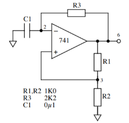
Astable Multivibrator:
There are two states as shown in figure and stable for a limited time. The circuit switches between them with the output (node 6) alternating between positive and negative saturation values ±VS.
Analysis of this circuit starts with the assumption that at time t = 0 the output has just switched to state 1 (V6 = +VS ), and the transition would have occurred when
A stable multivibrator
V2 = V6(state) R2/ R1 + R2 where V6(state0) = -Vs ----------------------(1)
In state 1, the voltage across the capacitor increases as a result of current flowing through R3 from its initial value
V2(t=0) = - Vs R2 / (R1 + R2) until
V2(to) = V3 (state 1) = +Vs . R2/ R1 + R2 --------------------------------------(2)
When the output from the op-amp switches back to state 0. Then the capacitor discharges until, at time t=2t0, the output switches from state 0 back to state 1 and the whole sequence restarts. It is straightforward to show that
To = C1 R3 ln(1 + 2 . R2 / R1)-------------------------------------------------(3)
Monostable Multivibrator
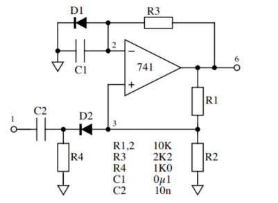
A diode is connected in parallel with the timing capacitor of the stable circuit which will prevent the inverting input of the amplifier from going positive as shown in the figure. The permanently stable state of this circuit has V6 = +Vs with node 2 clamped to approximately 0.6 V by diode D1 and node 3 at
V3 (state) = 0.6 V + Vs . R4/ R1 + R4 ---------------------------------------------(4)
Where it has been assumed that R2 >> R4 to simplify the expression. A sufficiently large pulse at node 3 is generated by a negative- going edge at the trigger input(node 1) which will switch the circuit into temporary state (V6= -Vs) after a delay
To = C1 R3 ln ( 1+ R2 / R1) ----------------------------------------------------(5)
Monostable Multivibrator
Bistable Multivibrator
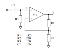
The circuit shows the op-amp configured as bistable multivibrator. The two stable states are V6 = ±Vss and the circuit is switched between these by a pulse of appropriate polarity applied to the inverting terminal (node 2) of the op-amp.
Square wave oscillator:
The basic square wave oscillator is based on charging and discharging of a capacitor. Op-amps inverting input is the capacitor voltage and the non-inverting input is a portion of the output fed back through resistors
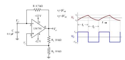
When the circuit is first turned on, the capacitor is uncharged, and thus the inverting input is at 0V. This makes the output a positive maximum, and the capacitor begins to charge towards voltage at VO through resistor R.
When the capacitor voltage reaches a value equal to the feedback voltage (Vf) on the non-inverting input, the op-amp switches to the maximum negative state.
At this point, the capacitor begins to discharge from +Vf towards –Vf.
When the capacitor voltage reaches –Vf, the op-amp switches back to the maximum positive state. This action repeats and a square wave output voltage is obtained.
Expression for period is
T = 2RC ln 1+β/ 1-β where β = R2/ R1 + R2
If R1= R2 the equation for period reduces to T = 2RC ln 3
The frequency of oscillation f = 1/ 2RC ln 3
Triangular-wave oscillator
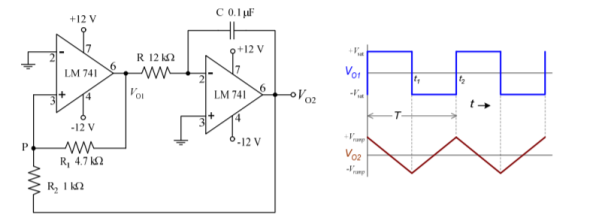
The figure uses two operational amplifiers.
- Op-amp A1 functions as a comparator
- Op-amp A2 as an integrator.
The Comparator compares the voltage at point P continuously with respect to the voltage at the inverting input which as at ground potential.
When the voltage at P goes slightly below zero, the output of A1 will switch to negative saturation. Suppose the output of A1 is at positive saturation +Vsat. Since this voltage is the input of the integrator, the output of A2 will be a negative going ramp.
Thus, one end of the voltage divider R1-R2 is at +Vsat and the other at the negative going ramp.
At time t = t1, when the negative going ramp attains value of –Vramp the effective voltage at point P becomes slightly less than 0 V. This switches output of A1 from positive saturation to negative saturation level –Vsat.
During the time when the output of A1 is at –Vsat, the output of A2 increases in positive direction. At the instant t = t2, the voltage at point P becomes just above 0 V, thereby switching the output of A1 from –Vsat to +Vsat. The cycle repeats and generates a triangular waveform.
At t=t1 -Vramp / R2 = - +Vsat / R1 that is - Vramp = - R2/R1 ( + Vsat)
Similarly at t=t2 + Vramp = -R2/ R1 ( - Vsat )
The peak to peak output of the triangular wave is
Vo (pp) = + Vramp- ( _ Vramp) = 2 R2/ R1 Vsat
During the period 0- t1 the integrator functions as below
Vo (p-p) = 1/ RC  = ( Vsat/ RC) ( T/2)
Then T = 2 RC ( Vo(p-p) / Vsat)
Substituting for Vo(p-p) T = 4RC R2/R1
Then the frequency of oscillation is given by
F = R1/ 4RC R2
Sawtooth-wave oscillator
The difference between the triangular and sawtooth waveform is that the rise time of the triangular wave is always equal to its fall time while in sawtooth wave generator, rise time may be much higher than its fall time or vice versa.
The triangular wave generator can be converted to a sawtooth wave generator by injecting a variable dc voltage into the non-inverting terminal of the integrator.
This can be done by using a potentiometer. When the wiper of the potentiometer is at the centre, the output will be a triangular wave since the duty cycle is 50%.
If the wiper moves towards –V, the rise time of the sawtooth becomes longer than the fall time.
If the wiper moves towards +V, the fall time becomes more than the rise time
Clipping circuits are used to clip off an unwanted portion of a waveform. Clipping circuits are called as limiting circuits. Limiting either positive or negative amplitude in large amplitude signal it is sometimes necessary to protect the device or circuit otherwise it may get damaged.
Depending on how the diode is placed in the circuit there are two types of clippers:
- Series clipper
- Shunt clipper
Series clipper:
A half-wave rectifier is considered as a clipper because it passes only half cycle and clips the other half cycle of the input. Therefore, series clipper is known as half-wave rectifier circuit.
Positive Series Clipper
When the positive half cycle of signal is clipped off from output it is called positive clipper. The input waveforms to the clipper can be sinusoidal or square or any other shape.
The series positive clipper is shown in the diagram below :

In series negative clipper, the negative half cycles of the input AC signal is removed at the output. The circuit construction of the series negative clipper is shown in the figure.
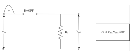
Case(i) : When the signal goes from 0 to π the diode becomes reverse biased since the cathode is at positive potential with respect anode and diode acts as an open circuit as shown in fig (a) the current i=0 in the loop so the output voltage is Vout =0 assuming diode is ideal with Vr =0, Rf =0 , RR = ∞
Case (ii): During the negative half cycle of input from π to 2π the diode is forward biased and the negative half cycle is passed to output. Because the cathode is negative with respect to anode and the diode is short circuit from input to output.
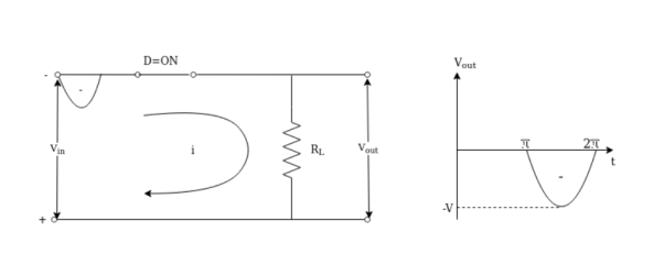
Vout = i RL
i = Vin / RL
Vout = Vin / RL x RL
Vout = Vin Since Vin = -V , Vout = -V .
Negative series clipper:
When the negative half cycle of the signal is clipped off from output it is called negative clipper. The negative series clipper is as shown in figure.
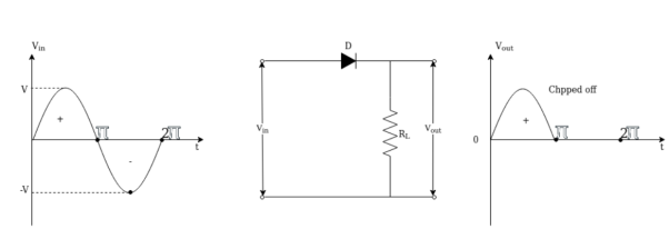
Case(i) During the positive half cycle of input from 0 to π diode D in forward biased and the positive half cycle is passed from input to output. Because the diode D anode is positive w.rt cathode the diode acts as short circuit as shown in figure (a)

Vout = i. RL
i = Vin / RL
Vout = Vin Since vin = +V ; Vout = +V
Case(ii) During the negative half cycle of input from π to 2π the diode is reverse biased and the output remains zero . Because diode D anode is negative w.r.t cathode diode acts as open circuit and the negative half cycle is clipped off as shown in figure

Shunt clipper:
Here the diode is connected in parallel with output port and these clippers are classified into :
- Positive shunt clipper
- Negative shunt clipper
Positive shunt clipper:
The figure shows a diode that limits or clips off the positive part of the input signal hence it is called positive shunt clipper.
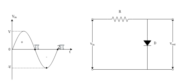
Case (i) : As the input Vin goes positive the diode D is forward biased due to the anode is positive w. r. t . Cathode and the diode is ON and acts as short across the output port as shown in fig (a) the positive half cycle is clipped off.

Case (ii) During the negative half cycle of input from π to 2π the diode is reverse biased because the diode anode is negative w.r.t cathode and diode acts as an open circuit as shown in fig(b).

Vin <0 ; Vout = Vin
Since diode acts as an open circuit across the output port and the drop across R is zero so the output voltage Vout = Vin .
Negative Shunt Clipper:
The negative shunt clipper is similar to positive shunt clipper only when the diode polarity reversed as shown in figure
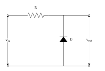
Case(i) :
During the positive half cycle of input from 0 to π, the diode D is reverse biased due to cathode is positive w.r.t. Anode and diode acts as open circuit and the input signal is transformed to output as shown in fig 2.7.8 (a)

Vout = Vin – i.R --------------------(1)
Since i=0
Vout = Vin
Since Vin >0 Vout = Vin.
Case (ii) : During the negative half cycle of input from π to 2 π the diode D is forward biased due to anode is positive w.r.t. Cathode and diode acts as short circuit. Thus the negative half cycle of waveform is clipped off as shown in fig (b) .

Dual clipper
Sometimes it is desired to remove a small portion of both positive and negative half cycles. In such cases, the dual clippers are used.
The dual clippers are made by combining the biased shunt positive clipper and biased shunt negative clipper.
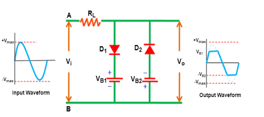
During the positive half cycle, the diode D1 is forward biased by the input supply voltage Vi and reverse biased by the battery voltage VB1. On the other hand, the diode D2 is reverse biased by both input supply voltage Vi and battery voltage VB2.
Initially, the input supply voltage is less than the battery voltage. So, D1 is reverse biased by the battery voltage VB1. Similarly, the diode D2 is reverse biased by the battery voltage VB2. As a result, the signal appears at the output.
However, when the input supply voltage Vi becomes greater than the battery voltage VB1, the diode D1 is forward biased by the input supply voltage. As a result, no signal appears at the output.
During the negative half cycle, the diode D1 is reverse biased by both input supply voltage Vi and battery voltage VB1. Diode D2 is forward biased by the input supply voltage Vi and reverse biased by the battery voltage VB2.
Initially, the battery voltage is greater than the input supply voltage. Therefore, the diode D1 and diode D2 are reverse biased by the battery voltage. As a result, the signal appears at the output.
When the input supply voltage becomes greater than the battery voltage VB2, the diode D2 is forward biased. As a result, no signal appears at the output.
Applications of clippers
Clippers are commonly used in power supplies.
Used in TV transmitters and Receivers
They are employed for different wave generation such as square, rectangular, or trapezoidal waves.
Series clippers are used as noise limiters in FM transmitters.
Problem:
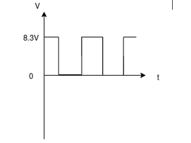
For a negative series clipper with zero load current shown below find a suitable resistor R1 and specify the diode forward current and reverse voltage for silicon diode. Sketch the output voltage waveform.
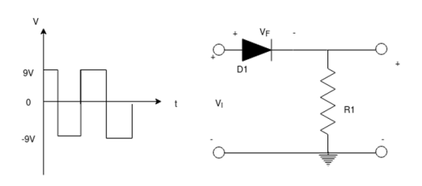
Solution:
When diode conducts
Vo = Vm – Vf
= 9-0.7 = 8.3 V
The diode forward current flows through R1
Vo = If R1
R1 = vo/If = 8.3 / If
When If = 1mA
R1 = 8.3/ 1mA = 8.3 kΩ.
During the negative half cycle of vi the diode is reverse biased by -vm . Therefore, the reverse voltage on the diode is
-Vr = -Vm = -9V
Vr = 9V.
Diode Specification
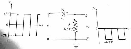
A positive series clipping circuit has ± 7V input and zero load current. Calculate a suitable resistor for R1 and specify the diode. Sketch the output voltage waveform.
Solution:
When diode conducts
Vo = -[Vm – Vf]
Assuming silicon diode
Vf = 0.7 V
Also Vm = 7V
Vo = -[7V – 0.7 V ] = - 6.3 V
R1 = vo/ If
= 6.3 / 1mA = 6.3 kΩ
Vr = Vm = 7V
Diode Specification
Vr = 7V
If = 1mA
The positive series clipper along with input and output waveforms is shown below.
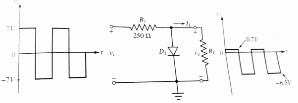
Problem: A positive shunt clipper of the figure has ± 7V input. The output voltage is to be -6. 5V when the load current is 2mA. Calculate the value of R1 and specify the diode forward current and reverse voltage.
Solution:
Given
Vm = 7V
Vo = -6.5 V IL = 2mA
The design equations of positive shunt clipper when diode is not conducting
R1 = vo + Vm /IL = -6.5 +7/ 2mA = 250Ω
Diode reverse voltage
Vr = Vm = 7V
When the diode is conducting
Vo = Vf = 0.7 V
IF = Vm – VF/R1 = 7 – 0.7 /250 = 25.2 mA
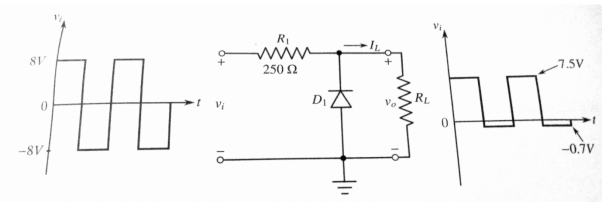
Problem: The negative shunt clipper as shown has ± 8V input and is to produce +7.5 V when the load current is 2mA. Find the suitable value of R1 and specify the diode forward current and reverse voltage.
Solution:
Given :
Vm = 8V
Vo = 7.5V
IL = 2mA
When the diode is not conducting
R1 = Vm -vo/IL = 8 -7.5 /2mA = 250Ω
Diode reverse voltage
Vr = Vm = 8V
When the diode is conducting
If = Vm -Vf/R1 = 8 – 0.7 / 250 = 29.2 mA
Vo = -Vf = -0.7V
The circuit of negative shunt clipper along with input and output waveforms is shown below.
Clamping circuits:
Clamping circuits are used to add or insert dc voltage level to a signal. A clamping circuit is called dc restorer since the dc voltage level lost in a signal can be recovered or restored by passing it through the clamping circuit.
Clamping operations can be understood with the following illustrations
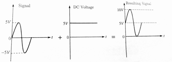
In the figure a 5V dc is added to a signal peak value of 5V. The resulting signal is completely positive, and its negative peak is clamped to zero volts. The operation is positive voltage clamping.
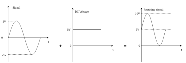
In the figure -5V dc is added to a signal of peak value of 5V. The resulting signal is completely negative, and its positive peak is clamped to zero volts. The operation is called negative voltage clamping.
Negative voltage clamping circuit:
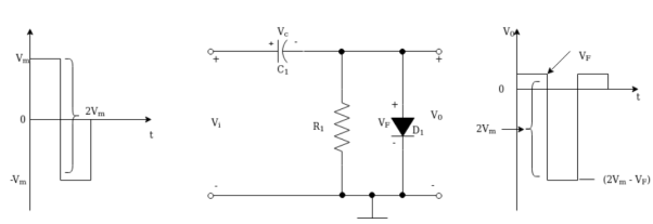
During the positive half cycle of input vi = Vm. The diode conducts and the charges the capacitor to Vm making the left plate positive.
Since the diode is connected between the output terminals
Vo = Vf
Applying KVL to the path consisting of vi,vc and VF we have
Vi – vc -Vf =0
Using vi = Vm we have
Vc = Vm -Vf
During the negative half cycle of the input vi = -Vm. The diode is reverse biased. The capacitor discharges into R!. The discharge is minimal as R1 is very high resistance. Hence, the capacitor voltage remains almost constant at
Vc = Vm – Vf
Apply KVL to the path consisting of vi,vc and vo we have
Vi – vc – vo = 0
Using vi = -Vm and vcVm -Vf we get
Vo = -(2Vm -Vf)
Peak to peak output voltage is
Vo(p-p) = VF – [-(2Vm -Vf)]
= 2Vm
Peak to peak input voltage is
Vi(p-p) = Vm –(-Vm)
= 2Vm
Therefore, vo(p-p) = vi(p-p)
Positive voltage clamping circuit
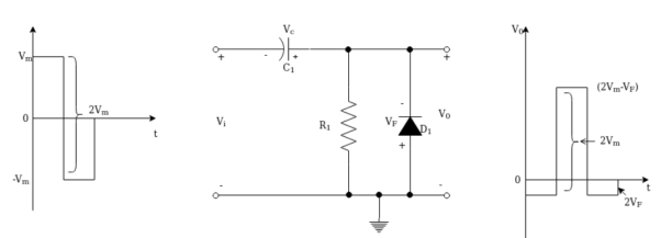
During the negative half cycle of the input signal vi = -Vm . The diode conducts and charges the capacitor to Vm making the right plate positive.
Since the diode is connected between the output terminals and the polarities of VF and Vo are opposite we have
Vo = -VF
Applying KVL to the path consisting of vi,vc and VF we have
Vi +vc + VF =0
Using vi = -Vm we have
Vc = vm -VF
During the positive half cycle of the input vi = -Vm. The diode is under reverse bias. The capacitor discharges into R1 is a very high resistance the discharge is minimal. Hence, the capacitor voltage remains almost constant at
Vc = Vm – VF
Apply KVL to the path consisting of vi,vc and vo we have
Vi + Vc -Vo =0
Using vi = Vm and vc = Vm-VF we have
Vm +Vm -Vf -vo =0
Or vo = 2Vm –Vf
Peak to peak output voltage
Vo(p-p) = (2Vm -Vf) –(-Vf)
= 2 Vm
Peak to peak input voltage is
Vi(p-p) = Vm –(-Vm)
= 2 Vm
Observe that vo(p-p) = vi(p-p)
The output waveform is completely positive with its negative peak clamped at -VF . Hence, the circuit is known as positive voltage clamping circuit.
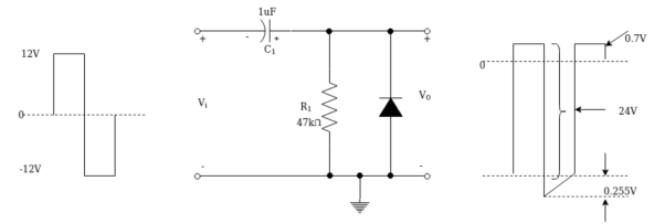
Problem: The input to the negative clamping clamping circuit is as shown in the figure which is at ±12V , 1kHz square wave . If R1= 47kΩ and C1 = 1µF. Calculate the tilt in the output waveform . Draw the circuit and sketch the input and output waveform.
Solution :
Vm = 12V f = 1kHz T = 1/f = 1msec. R1 = 47kΩ and C1 = 1µF.
The tilt in the waveform is given by
∆ vc = Ic x t / C1
Ic ≈ vo(p-p) / R1 = 2Vm /R1 =24 / 47 k = 510.64 µ A.
t=T/2 = 0.5 ms = 500 µ s
∆ vc = 510.64 µ x 500 µ / 1 µ = 255.32 mV.
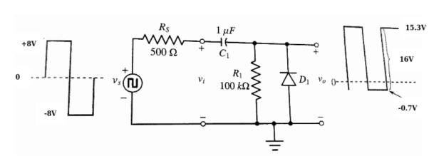
The positive voltage clamping circuit has ±8V, 1kHz square wave with 500Ω source resistance. The output is to have a maximum tilt of 0.5 % . Calculate suitable values of R1 and C1 . Draw the circuit and sketch the input and output waveform.
Vm = 8V . f = 1kHz. T = 1ms ; Rs = 500Ω ∆vc = 0.5% of vo(p-p)
Vo(p-p) = 2Vm =16V
∆ vc = 0.08V
PW = t = T/2 = 0.5msec
C1 = PW/Rs = 0.5 mS /500 Ω = 1µF
Ic = ∆vc x C1/t = 0.08 x 1µF / 0.5 mS = 0.16mA or 160 µ A
R1 = 2Vm/Ic = 16V /0.16 mA = 100KΩ
The positive voltage clamping circuit with its input and out put waveform.
Definition:
Peak detector circuits are used to determine the peak (maximum) value of an input signal.
It stores the peak value of input voltages for infinite time duration until it comes to reset condition.
The peak detector circuit utilizes its property of following the highest value of an input signal and storing it.
Circuit Working of Peak detector
The figure below shows the circuit of a basic positive peak detector-
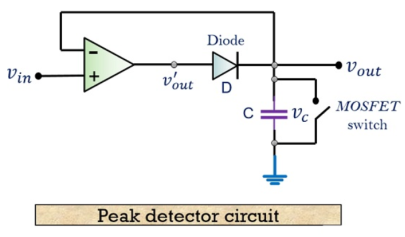
The circuit consists of a diode and capacitor along with an op-amp as shown in the figure.
Working Principle
The working principle of the circuit is such that, the peak of the input waveform is followed and stored in terms of voltage in the capacitor.
During the following interval if the circuit detects a higher peak, the new peak value is stored in the capacitor until it is discharged.
The capacitor employed in the circuit is charged through the diode by the applied input signal.
The small voltage drop across the diode is ignored and the capacitor is charged up to the highest peak of the applied input signal.
Let us consider initially the capacitor is charged to voltage Vc. The diode employed in the circuit gets forward biased when the applied input voltage Vin exceeds the capacitor voltage Vc. Thereby allowing the circuit to behave as a voltage follower. The output voltage follows the applied input voltage until Vin is more than Vc.
As the input voltage Vin reduces below the value of capacitive voltage Vc, it causes the diode to get reverse biased. In such condition, the capacitor retains the value until the input again exceeds the value stored in the capacitor.
The figure below shows the output voltage waveform for an applied input signal.
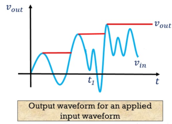
From the figure at time t1, the circuit misses the peak of the input signal as it is less than the previous peak of the input signal. Thereby allowing the capacitor to hold the value of the previously occurred peak.
As it is a positive peak detector, one can also construct a negative peak detector circuit, that will hold the lowest or most negative signal voltage. This is basically done by reversing the polarities of the diode in the circuit.
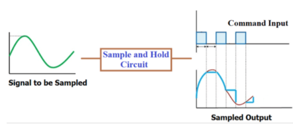
Sample and Hold Circuit takes samples from the analog input signal and hold them for particular period of time and then outputs the sampled part of input signal.
It consists of switching devices, capacitor, and an operational amplifier.
The capacitor is the heart of the Sample and Hold Circuit because it holds the sampled input signal and provides it at the output. This circuit is mostly used in Analog to Digital Converters to remove certain variations in input signal, which may corrupt conversion process.
A typical block diagram of Sample and hold circuit is mentioned below:
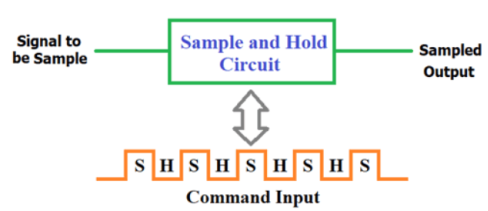
Generally applied input voltage signal is a continuously changing analog signal. Command input is provided to trigger the sampling and holding of input signal.
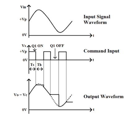
Command input is nothing but on/off signal to start/stop sampling of input signal, it is generally PWM. The sampling and holding process depends on the command input. When the switch is closed the signal is sampled and when its open the circuit holds the output signal. The On/OFF condition of switch is controlled by command input.
The ideal input and output waveform of the sample and hold circuit is given below:
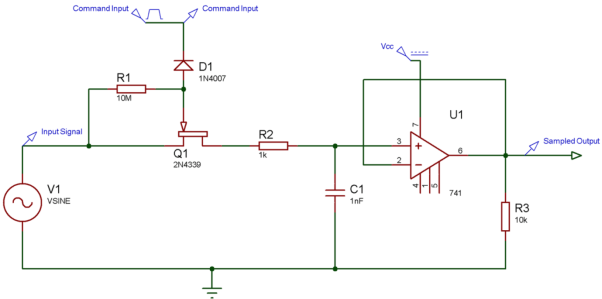
Circuit Diagram
Working of Sample and Hold Circuit
The circuit consists of 2N4339 N-channel JFET, an op-amp, and a capacitor.
A command input (a PWM input) is connected to the Gate terminal of the 2N4339 transistor hence 2N4339 N-channel JFET, an op-amp, and a capacitor.
Whenever the command input voltage is negative the diode will be forward biased which cause the transistor to turns ON and vice versa.
The Op-amp 741 is used as voltage follower because voltage follower generally has a high input impedance and a low output impedance. This is used when the input signal is of low current because voltage follower can supply sufficient current to the next stage.
So, whenever the command input is HIGH the transistor works as closed switch and at this moment the capacitor starts charging to its peak value and stores the sample of input signal for the time transistor is in on state.
Now when the command input is LOW the transistor works as open switch and the capacitor will experience high impedance and due to this it cannot get discharged and holds the charge for a particular period of time.
This time is known as Holding Period and the time during which the circuit samples the input signal is called as the Sampling Period.
Some Applications of Sample and Hold Circuit
- ADCs (Analog-to-Digital Conversion)
- DACs (Digital-to-Analog Conversion)
- In Analog Demultiplexing
- In Linear Systems
- In Data Distribution System
- In Digital Voltmeters
- In Signal Constructional Filters
R-2R ladder network
A D/A converter with R and 2R resistors is shown in the figure. The binary inputs are given through the switches b0-b3and output is proportional to the binary inputs.
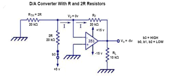
Binary inputs are either HIGH (+5V) or LOW (0V) state. Let b3 be the MSB which is connected to +5V and all the other switches are connected to the ground.
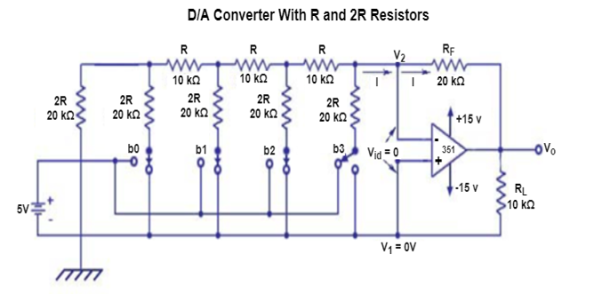
Thus, according to Thevenin’s equivalent resistance, RTH,
RTH = [{[(2R ||2R + R)} ||2R] + R}||2R] + R = 2R = 20kOhms.
The resultant circuit is shown below.
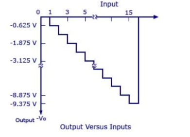
Graph is given below.
In the figure shown above, the negative input is at virtual ground, therefore the current through RTH=0.
Current through 2R connected to +5V = 5V/20kohm = 0.25 mA
The current will be the same as that in Rf.
Vo = -(20kohm)*(0.25mA) = -5V
Output voltage equation is given below.
V0 = -Rf (b3/2R+b2/4R+b1/8R+b0/16R)
Binary weighted resistor DAC:
A weighted resistor DAC produces an analog output, which is almost equal to the digital (binary) input by using binary weighted resistors in the inverting adder circuit.
In short, a binary weighted resistor DAC is called as weighted resistor DAC.
The circuit diagram of a 3-bit binary weighted resistor DAC is shown in the following figure −
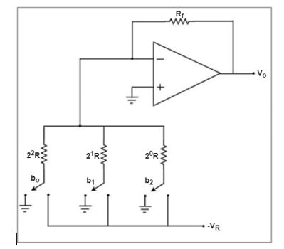
Letthe 3-bit binary input is b2b1b0. Here, the bits b2 and b0 denote the Most Significant Bit (MSB) and Least Significant Bit (LSB) respectively.
The digital switches shown in the above figure are connected to ground, when the corresponding input bits are equal to ‘0’. Similarly, the digital switches shown are connected to the negative reference voltage−VR when the corresponding input bits are equal to ‘1’.
In the above circuit, the non-inverting input terminal of an op-amp is connected to ground. That means zero volts is applied at the non-inverting input terminal of op-amp.
According to the virtual short concept, the voltage at the inverting input terminal of op-amp is same as that of the voltage present at its non-inverting input terminal. So, the voltage at the inverting input terminal’s node will be zero volts.
The nodal equation at the inverting input terminal’s node is:
0 + VR b2 / 2 0 R + 0 + VR b1 / 2 1 R + 0 + VRbo / 2 2 R + 0 – Vo / Rf =0
Vo / Rf = VR b2 / 20 R + VR b1 / 2 1 R + VR bo / 2 2 R
--- V0 = VR Rf/ R { b2 / 20 + b1/ 2 1 + bo / 2 2 }
Substituting R = 2 Rf in the above equation
Vo = VR Rf/ 2 Rf { b2 / 2 0 + b1 / 2 1 + bo / 2 2 }
Vo = VR / 2 { b2 / 2 0 + b1 / 2 1 + bo / 2 2 }
The above equation represents the output voltage equation of a 3-bit binary weighted resistor DAC.
Since the number of bits are three in the binary (digital) input, there are seven possible values of output voltage by varying the binary input from 000 to 111 for a fixed reference voltage, VR.
Problem:
The generalized output voltage equation of an N-bit binary weighted resistor DAC as shown below based is given by
--- Vo = VR/2 { b N-1 / 20 + b N-2 / 2 1 +………….+ bo / 2 N-1 }
A certain 8-bit DAC has a full-scale output of 2mA and a full-scale error of ± 0.5% F.S. What is the range of possible outputs for an input of 10000000?
Solution:
The step size is 2mA/255 = 7.84 µA. Since 10000000 = 12810, the ideal output should be 128 × 7.84 µA.
The error can be as much as ± 0.5% × 2mA = ± 10µA Thus, the actual output can deviate by this amount from the ideal 1004µA, so the actual output can be anywhere from 994 to 1014 µA.
An analog-to-digital converter takes an analog input voltage and after a certain amount of time produces a digital output code which represents the analog input. The A/D conversion process is generally more complex and time-consuming than the D/A process.
The techniques that are used provide and insight into what factors determine an ADCs performance.
Several important types of ADC utilize a DAC as part of their circuitry.
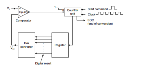
The Figure represents the general block diagramof ADC. The timing for the operation is provided by the input clock signal. The control unit contains the logic circuitry for generating the proper sequence of operations.
The START COMMAND, initiates the conversion process, The op-amp comparator has two analog inputs and a digital output that switches states, depending on which analog input is greater.
The basic operation of ADCs of this type consists of the following steps:
1. The START COMMAND pulse initiates the operation.
2. At a rate determined by the clock, the control unit continually modifies the binary number that is stored in the register.
3. The binary number in the register is converted to an analog voltage, VAX, by the DAC.
4. The comparator compares VAX with the analog input VA. If VAX < VA1 the comparator output stays HIGH.When VAX exceeds VA by at least an amount = VT ( threshold voltage), the comparator output goes LOW and stops the process of modifying the register number.
At this point, VAX is a close approximation to VA.
The digital number in the register, which is the digital equivalent of VAX, is also the approximate digital equivalent of VA1 within the resolution and accuracy of the system.
5. The control logic activates the end-of-conversion signal, EOC, when the conversion is complete.
One of the simplest versions of the general ADC as shown in figure which uses a binary counter as the register and allows the clock to increment the counter one step at a time until VAX ≥ VA. It is called a digital-ramp ADC because the wave form at VAX is a step-by-step ramp (actually a staircase) like the one shown in Figure. It is also referred to as a counter-type ADC.
Figure represents the diagram for a digital-ramp ADC.
It contains a counter, a DAC, an analog comparator, and a control AND gate.
The comparator output serves as the active-LOW end-of conversion signal, EOC . If we assume that VA, the analog voltage has to be converted, is positive, the operation proceeds as follows :
1. A START pulse is applied to reset the counter to zero. The HIGH at START also inhibits clock pulse form passing through the AND gate into the counter.
2. With all 0’s at its input, the DAC’s output will be VAX = 0V.
3. Since VA > VAX, the comparator output, EOC , will be HIGH.
4. When START returns LOW, the AND gate is enabled and clock pulses get through to the counter. 5. As the counter advances, the DAC output, VAX, increases one step at a time as shown in Figure.
6. This continues unit VAX reaches a step that exceeds VA by an amount equal to or greater than VT (typically 10 to 100 µV). At this point, EOC will go LOW and inhibit the flow of pulses into the counter and the counter will stop counting.
7. The conversion process is now complete as signalled by the HIGH-to-LOW transition at EOC , and the contents of the counter are the digital representation of VA.
8. The counter will hold the digital value until the next START pulse initiates a new conversion.
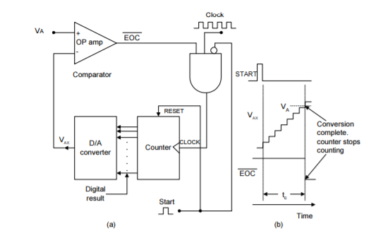
Digital ramp ADC
References:
Basic Electronics (VTU) by Professor D Chattopadhyay , Professor P C Rakshit, New Age International (P) Ltd., Publishers
Basic Electronics By Theraja B.L.
CIRCUIT FUNDAMENTALS and BASIC ELECTRONICS Ashish Chaudhury and R. K. Verma.
Basic Electronics by D P Kothari, I J Nagrath