Unit 1
Introduction to Microprocessor Systems
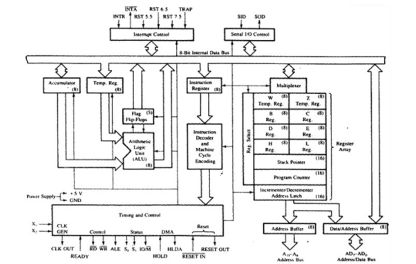
8085 consists of the following functional units −
Accumulator
The accumulator is an 8-bit register used to perform arithmetic, logical, I/O & LOAD/STORE operations. It is connected to internal data bus & ALU.
Arithmetic and logic unit
The arithmetic and logic unit performs arithmetic and logical operations like Addition, Subtraction, AND, OR, etc. on 8-bit data.
General purpose register
8085 consists of six general purpose registers in 8085 processor that is B, C, D, E, H & L. Each register holds 8-bit data. These registers work in pair to hold 16-bit data and their pairing combination is like B-C, D-E & H-L.
Program counter
It is a 16-bit register used to store the memory address location of the next instruction to be executed. Microprocessor increments the program whenever an instruction is being executed, so that the program counter points to the memory address of the next instruction that is going to be executed.
Stack pointer
It is 16-bit register which works like stack, which gets incremented/decremented by 2 during push & pop operations.
Temporary register
It is an 8-bit register, which holds the temporary data of arithmetic and logical operations.
Flag register
It is an 8-bit register which holds 0 or 1 depending upon the result stored in the accumulator.
These are : −
- Sign (S)
- Zero (Z)
- Auxiliary Carry (AC)
- Parity (P)
- Carry (C)

Instruction register and decoder
It is an 8-bit register. When an instruction is fetched from memory then it is stored in the Instruction register. Instruction decoder decodes the information present in the Instruction register.
Timing and control unit
It provides timing and control signal to the microprocessor to perform operations. Following are the timing and control signals, which control external and internal circuits −
- Control Signals: READY, RD’, WR’, ALE
- Status Signals: S0, S1, IO/M’
- DMA Signals: HOLD, HLDA
- RESET Signals: RESET IN, RESET OUT
Interrupt control
It controls the interrupts during the process. When the microprocessor is executing the main program and whenever an interrupt occurs, the microprocessor shifts the control from the main program to process the incoming request. After the request is completed, the control returns to the main program.
There are 5 interrupt signals in 8085 microprocessors:
- INTR
- RST 7.5
- RST 6.5
- RST 5.5
- TRAP.
Serial Input/output control
It controls the serial data communication by using the two instructions: SID (Serial input data) and SOD (Serial output data).
Address buffer and address-data buffer
The content stored in the stack pointer and program counter is loaded into the address buffer and address-data buffer to communicate with the CPU.
The memory and I/O chips are connected to these buses, the CPU can exchange the desired data with the memory and I/O chips.
Address bus and data bus
Data bus carries the data to be stored. It is bidirectional whereas address bus carries the location to where it should be stored, and it is unidirectional. It is used to transfer the data & Address I/O devices.
Pin Diagram of 8085
The 40 pins of microprocessor can be divided into six groups such as
- Address bus
- Data bus
- Control signals & status signals
- Power supply & frequency
- Externally started signals
- Serial input/output ports.
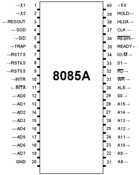
8085 Microprocessor pin Configuration
Address Bus (A8-A15)
The address bus pins A8 to A15 are applicable to the most considerable memory address bit.
Address Bus (or) Data Bus (AD0-AD7)
The address bus pins or data bus pins ranges from AD0 to AD7, and these pins are applicable for LSB (least significant bits) of the address bus in the primary apparatus CLK cycle as well as employed as a data bus for second clock cycle & third clock cycle.
A CLK cycle is designed as time in use among two oscillator’s nearby pulses, or simply it can refer to zero volts. Here the first clock is the primary transition of pulse ranges from 0V to 5V & then reaches back to 0V.
Address Latch Enable (ALE)
ALE (Address Enable Latch) is the control signal a positive going pulse generated when a new operation is started by microprocessor. So, when pulse goes high means ALE=1, it makes address bus enable and when ALE=0, means low pulse makes data bus enable.
Status Signal (IO/M)
The status signal IO/M resolves whether the address is intended for memory or input/output. When the address is high then the address of the address bus is used for the devices of input/output devices. When the address is low then the address of the address bus is used for the memory.
Status Signals (S0-S1)
The status signals S0, S1 gives different functions as well as status based on their status.
- When the S0, S1 are 01 then the operation will be HALT.
- The S0, S1 is 10 then the operation will be WRITE
- When the S0, S1 is 10 then the operation will be READ
- When the S0, S1 are 11 then the operation will be FETCH
Active Low Signal (RD)
This signal indicates that the selected IO or memory device is to be read and is ready for accepting data available on the data bus.
Active low signal WR
This signal indicates that the data on the data bus is to be written into a selected memory or IO location.
READY
The READY pin is employed for ensuring whether a device is set for accepting or transferring data.
A device may be an A/D converter or LCD display, etc. These devices are associated with the 8085 microprocessors with the READY pin.
When this pin is high, the device is prepared for transferring the information, if it is not then the microprocessor stays until this pin goes high.
HOLD
The signal indicates that another master is requesting the use of address and data buses.
HLDA (Hold Acknowledge)
This signal indicates that CPU has received the HOLD request and it will relinquish the bus in the next clock cycle. HLDA is set to low after HOLD signal is removed.
INTR
This is an interrupt signal, and the priority of this among the interrupt is low. This signal can be allowed or not allowed by the software. When INTR pin goes high then the 8085 microprocessor completes the instruction of current which is being executed and then recognizes the INTR signal and progresses it.
INTA
When the 8085 microprocessor gets an interrupt signal, then it should be recognized. This will be done by INTA. As a result, when the interrupt will be obtained then INTA will go high.
RST 5.5, RST 6.5, RST 7.5
These pins are the restart maskable interrupts or Vectored Interrupts, used to insert an inner restart function repeatedly. All these interrupts are maskable, they can be allowed or not allowed by using programs.
TRAP
Along with the 8085 microprocessor interrupts, TRAP is a non-maskable interrupt, and it doesn’t allow or stopped by a program. TRAP has the maximum precedence between the interrupts. The priority order from maximum to low includes TRAP, RST 5.5, RST 6.5, RST 7.5, and INTR.
RESET IN
RESET IN pin is used to reset the program counter toward zero and rearranges interrupt enable as well as HLDA flip flops (FFs). The central processing unit is detained in RST condition till this pin is high. But the registers as well as flags won’t get damaged apart from instruction register.
RST (RESET) OUT
RESET OUT pin specifies that the central processing unit has been rearranged with RST IN.
X1 X2
X1, X2 terminals that are associated with the exterior oscillator for generating the required as well as appropriate operation of a clock.
CLK
Sometimes it is compulsory to generate CLK o/PS from 8085 microprocessors so they can be used in favor of other peripherals or else other digital integrated circuits. This is offered with CLK pin. Its frequency is continually similar because the frequency at which the microprocessor works.
SID
This is a serial i/p data, and the information on this pin is uploaded into the 7th-bit of the accumulator while RIM (Read Interrupt Mask) instruction is performed. RIM verifies the interrupt whether it is covered or not covered.
SOD
This is the serial o/p data, and the data on this pin sends its output toward the 7th-bit of the accumulator whenever an instruction of SIM is performed.
VSS and VCC
VSS is a ground pin whereas Vcc is +5v pin.
- Timing diagram helps to understand the working of any system step by step and working of each instruction, its decoding, fetching and execution.
- It is the graphical representation with respect to time.
- It represents the clock cycle with duration, delay, content of address bus and data bus, type of operation w.r.to Read/write/status signals.
Important terms used
1. Instruction cycle: It is defined as the number of steps required by the CPU to complete the process which includes fetching, decoding and execution of one instruction. They are carried out in synchronization with the clock pulse.
2. Machine cycle: It is the time required by the microprocessor to complete the operation of accessing the memory or I/O devices. Here, operations like opcode fetch, memory read, memory write, I/O read and I/O write can be performed.
3. T-state: Each clock cycle is known as T-state.
Rules to identify number of machine cycles in an instruction:
1. If an addressing mode is direct, immediate or implicit then
No. Of machine cycles = No. Of bytes.
2. If the addressing mode is indirect then
No. Of machine cycles = No. Of bytes + 1.
Add +1 to the No. Of machine cycles if it is memory read/write operation.
3. If the operand is 8-bit or 16-bit address then,
No. Of machine cycles = No. Of bytes +1.
4. These rules are applicable to 80% of the instructions of 8085.

Fig.1: Timing Diagram
Fetch cycle
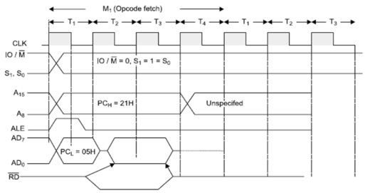
Fetch Cycle
- The microprocessor requires instructions to perform any particular task. In order to perform these tasks it utilizes Opcode which is a part of an instruction which provides detail to the microprocessor.
 During T1 state, microprocessor uses IO/M, S0, S1 signals are used to instruct microprocessor to fetch opcode.
 Thus when IO/M =0 and S0=S1= 1, it indicates opcode fetch operation.
During this operation 8085 transmits 16-bit address and also uses ALE signal for address latching.
At T2 state, microprocessor uses read signal and make data ready from that memory location to read opcode from memory and at the same time program counter is incremented by 1 and points next instruction to be fetched.
In this state microprocessor also checks READY input signal, if this pin is at low logic level ie. '0' then microprocessor adds wait state immediately between T2 and T3.
At T3 state, microprocessor reads the opcode and stores it into instruction register to decode it further.
At T4 state, the microprocessor performs internal operation like decoding opcode and providing necessary actions.
The opcode is decoded to know whether T5 or T6 states are required or not for next operation.
Read Cycle
1. Memory read
2. I/O read
Memory Read
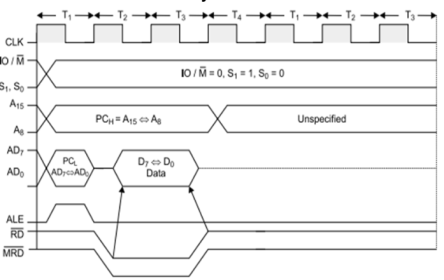
Memory read Cycle
It fetches one byte from the memory at a time.
It requires 3 T-States.
It is used to fetch operand or data from the memory.
During T1 state, A8-A15 contains higher byte of address, ALE is high therefore lower byte of address A0-A7 is selected from the multiplexed lines AD0-AD7.
 Since it is a memory ready operation, IO/M =0.
 During T2state, ALE = 0, RD = 0 and address is removed from AD0-AD7 and data D0-D7 appears on the lines AD0-AD7.
 During T3 state, data remains on AD0-AD7 till , RD = 0.
I/O Read
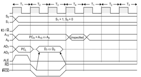
I/O read Cycle


 It is used to fetch one byte from an IO port at a time.
It requires 3 T-States.
During T1 state, the lower Byte of IO address is copied into higher order address bus A8-A15.
ALE = 1 and AD0-AD7 contains address of IO device.
IO/M = 1 as it is an IO operation.
During T2 state, ALE = 0, RD = 0 and data appears on AD0-AD7 as input from IO device.
During T3 state, data remains on AD0-AD7 till RD = 0.
Write Cycle
1. Memory write
2. I/O write
Memory write cycle
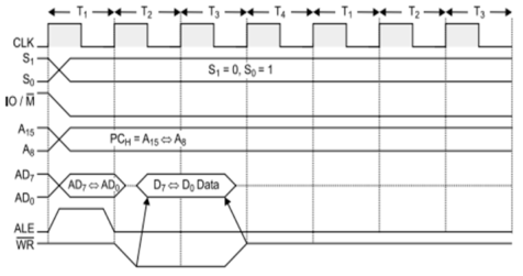
Memory write Cycle
It is used to send one byte at a time into memory.
It requires 3 T-States.
During T1 state, ALE = 1 and contains lower address A0-A7 from multiplexed lines AD0-AD7 and A8-A15 contains higher byte of address.

 As it is memory operation, IO/M = 0.
 During T2 state, ALE = 0, WR = 0 and address is removed from AD0-AD7 and data appears on AD0-AD7.
- Data remains on AD0-AD7 till WR = 0.
I/O write cycle
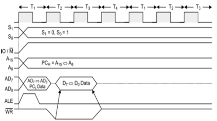
I/O write Cycle
It is used to write one byte at a time into IO device.
It requires 3 T-States.
During T1 state, the lower byte of address is copied into higher order address bus A8-A15.
ALE =1 and A0-A7 address is selected from the multipled lines AD0-AD7.
 As it is an IO operation, IO/M = 1.
 During T2 state, ALE = 0, WR = 0 and data appears on AD0-AD7 to write data into IO device.
 During T3 state, data remains on AD0-AD7 till WR = 0.
The memory is used to store information used by the CPU.
The information can be in the form of program that the CPU executes or data on which the CPU operates.
Memory can be classified into two groups.
1- Primary Memory
2- Secondary Memory
Primary Memory
It is that part of the memory which can be directly access by the CPU. It can be viewed as a stack of words, each word be associated with a unique address. These words may be instruction or data. A CPU having n address line can access 2n memory location. The total primary memory area is partition into two separate sections called the ROM area and the read/write area.
ROM
When CPU is turned ON or reset, it starts executing the program from a fixed default address which is usually the first address of the address space. These instructions initialize the sequences which directs the CPU to initialize all sub systems. For example CPU may initialize the display driver display outputs in a particular manner or initialize a key-board to accept the certain commands.
It has to perform each time computer begins its operation and is part of the monitor software which is stored in the permanent or non-volatile memory. The program is not lost when the power is switched off and it is available each time the power is switched on. It is implemented by using a special kind of memory called read only memory or ROM. The data cannot be written over and can only the read. The ROM is used to store information that should not change. ROMs are available into 4 types. They are
i. Masked ROM
Ii. PROM
Iii. EPROM
Iv. EEPROM
i-Masked ROM
The instructions here are permanently installed by the manufacturer as for the
Specification provided by the system programmer and cannot be altered. This ROM contains
Call arrays in which 1s and 0s are stored by means of a metallization interconnect most
At the time of fabrication.
Ii-PROM (Programmable Read Only Memory)
Here, the manufacturer provides a memory device which can be programmed by the user by using a PROM program. The PROM uses a fusible links that can be burnt or melted by special PROM burning circuit. A fused link is corresponding to zero.
Iii-EPROM (Erasable PROM)
It uses most charge storage technology. It is also programmable by the user. The information
Stored in the EPROM can be erased by exposing the memory to ultraviolet light which erase
The data stored the data in total memory area. Then the memory can be reprogrammable by
The user by using EPROM burning circuit.
Iv-EEPROM (Electrically Erasable PROM)
This is similar to EPROM except that the erasing done by electrical signal instead of
Ultraviolet light and that the data in memory location can be selective erased.
Read/Write Area
It is a special kind of memory area where information can be written or read whenever necessary. The CPU uses this section memory as a scratch pad memory. It is also called random access memory or RAM. The CPU can access any memory location by specifying its address. Unlike ROM the conventional is a volatile memory i.e. the contents of the RAM
Are used when the power is switched off. RAMs are two types.
i-Static RAM
Here, once the data is written into a memory location, the data remain unchanged unless on same memory location is written into again. It uses flip-flops for storage elements.
Ii-Dynamic RAM
Here, the basic storage element is a capacitor. This element contains a 1or a 0 depending on the presence or absence of charge. Unlike static RAM, the contents of the dynamic RAM may change with time due to leakage of charge. So it is necessary to periodically refresh the storage element in a dynamic RAM. Here it has external refresh circuitry.
The advantages of dynamic RAM over static RAM :
It consumes less power than static RAM.
It has about 5 times more storage element per unit area.
Disadvantages:
DRAMS have slower access times and need special circuitry to periodically refresh memory.
i-RAMs:
RAMs are also implemented using other technologies like i-RAM (integrated RAM) which
Are dynamic RAM devices in which the memory refresh circuitry is implemented within the
Device.
Bubble Memories
It is a type of DRAM. Here the contents are not lost when the power is switched off.
Secondary Memory
The maximum capacity of primary memory is 2n location. Each of 2n location where n is the
Number of CPU address lines. Sometimes it is necessary to handle more data than allowed by
The primary memory. In such cases secondary memory is used. The CPU cannot directly
Access memory but can access through I/O ports.
These are the instructions used to transfer the data from one register to another register, from the memory to the register, and from the register to the memory without any alteration in the content. Addressing modes in 8085 is classified into 5 groups −
Immediate addressing mode
In this mode, the 8/16-bit data is specified in the instruction itself as one of its operand. For example: MVI K, 20F: means 20F is copied into register K.
Register addressing mode
In this mode, the data is copied from one register to another. For example: MOV K, B: means data in register B is copied to register K.
Direct addressing mode
In this mode, the data is directly copied from the given address to the register. For example: LDB 5000K: means the data at address 5000K is copied to register B.
Indirect addressing mode
In this mode, the data is transferred from one register to another by using the address pointed by the register. For example: MOV K, B: means data is transferred from the memory address pointed by the register to the register K.
2 Implied addressing mode
3 This mode doesn’t require any operand; the data is specified by the opcode itself. For example: CMP.
3.1 Interrupts
Interrupt is signals send by an external device to the processor, to request the processor to perform a particular task Mainly in the microprocessor based system the interrupts are used for data transfer between the peripheral and the microprocessor.
The processor will check the interrupts always at the 2nd T-state of last machine cycle.
If there is any interrupt it will accept the interrupt and send the INTA (active low) signal to the peripheral.
The vectored address of interrupt is stored in program counter.
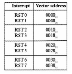
The processor executes an interrupt service routine (ISR) addressed in program counter. It returned to main program by RET instruction.
Types of Interrupts: It supports two types of interrupts.
1. Hardware interrupts
2. Software interrupts
Software interrupts: The software interrupts are program instructions. These instructions are inserted at desired locations in a program. The 8085 has eight software interrupts from RST 0 to RST 7. The vector address for these interrupts can be calculated as follows. The Table shows the vector addresses of all interrupts.
Hardware interrupts: An external device initiates the hardware interrupts and placing an appropriate signal at the interrupt pin of the processor. If the interrupt is accepted, then the processor executes an interrupt service routine.
3.2 Assembly Language Programming
Machine language and Hex code instructions are difficult for the programmer. Hence for programmer, the instructions of microprocessor are made in the form of English abbreviation (short form).
These instructions are name as Assembly Language instructions or mnemonics. The combinations of different mnemonics are known as Assembly Language Program and it is a low- level language.
Write a program to transfer 07 H in register L
Memory address | Machine Code | Mnemonics | Operands | Comments |
2000H | 2E,07 | MVI | L,07 | Move immediate 07 in register L |
2002H | 76 | HLT |
| Stop or terminate the program |
The instruction MVI L, 07 will move the data 07 to the register L. The instruction will stop the program. The machine code for the instruction MVI L, 07 is 2E, 07. The 1st byte of the machine code is 2E which is the Hex code for the instruction MVI L. The second byte is the data 07.
The machine code for HLT is 76.
The machine codes are fetch in the memory locations, starting from the memory locations 2000 H. Memory location 2000 H contains 2E, 2001 H contains 07 and memory location 2002 H contain 76.
After the execution of a program, the contents of Register L can be examined which are 07.
3.3 8085 Interrupts
The 8085 has five hardware interrupts
(1) TRAP
(2) RST 7.5
(3) RST 6.5
4) RST 5.5
5) INTR
TRAP: This interrupt is a non-maskable interrupt. It is unaffected by any mask or interrupt enable. TRAP has the highest priority and vectored interrupt. TRAP interrupt is edge and level triggered. This means hat the TRAP must go high and remain high until it is acknowledged. In sudden power failure, it executes a ISR and send the data from main memory to backup memory. The signal, which overrides the TRAP, is HOLD signal. (i.e., If the processor receives HOLD and TRAP at the same time then HOLD is recognized first and then TRAP is recognized).
There are two ways to clear TRAP interrupt.
1. By resetting microprocessor (External signal)
2. By giving a high TRAP ACKNOWLEDGE (Internal signal)
RST 7.5: The RST 7.5 interrupt is a maskable interrupt. It has the second highest priority. It is edge sensitive. Ie. Input goes to high and no need to maintain high state until it recognized. Maskable interrupt. It is disabled by,
1. DI instruction
2. System or processor reset.
3. After reorganization of interrupt.
Enabled by EI instruction.
RST 6.5 and 5.5: The RST 6.5 and RST 5.5 both are level triggered. Ie. Inputs goes to high and stay high until it recognized.
Maskable interrupt. It is disabled by,
1.DI, SIM instruction
2.System or processor reset.
3. After reorganization of interrupt. Enabled by EI instruction. The RST 6.5 has the third priority whereas RST 5.5 has the fourth priority.
INTR: INTR is a maskable interrupt. It is disabled by,
1.DI, SIM instruction
2.System or processor reset.
3.After reorganization of interrupt.
Enabled by EI instruction. Non- vectored interrupt. After receiving INTA (active low) signal, it has to supply the address of ISR. It has lowest priority. It is a level sensitive interrupts. Ie. Input goes to high and it is necessary to maintain high state until it recognized.
The following sequence of events occurs when INTR signal goes high.
1. The 8085 checks the status of INTR signal during execution of each instruction.
2. If INTR signal is high, then 8085 complete its current instruction and sends active low interrupt acknowledge signal, if the interrupt is enabled.
3. In response to the acknowledge signal, external logic places an instruction OPCODE on the data bus. In the case of multibyte instruction, additional interrupt acknowledge machine cycles are generated by the 8085 to transfer the additional bytes into the microprocessor.
4. On receiving the instruction, the 8085 save the address of next instruction on stack and execute received instruction.
An interface is a concept that refers to a point of interaction between components which is applicable at the level of both hardware and software.
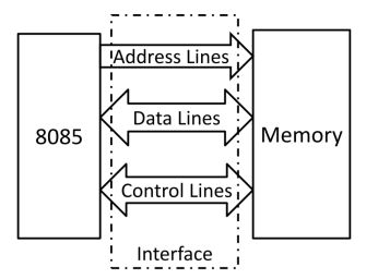
Memory are made up of registers
Each register contains one storage location
Each location consists of address
The total number of memory storage is called memory capacity and measured in bytes .
Storage element is called cell.
The data could be read or written from memory.
References:
Microprocessor Architecture, Programming, and Applications with the 8085 Textbook by Ramesh S. Gaonkar
Microprocessor 8085 and Its Interfacing Book by Mathur Sunil
8085 MICROPROCESSORS: PROGRAMMING AND INTERFACING
Book by N. K. SRINATH