Unit 3
Introduction to 8086,80286,80386,80846
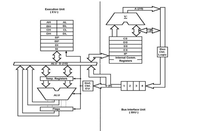
8086, it is a 16-bit Integer processor in a 40 pin, Dual Inline Packaged IC.
The size of the internal registers indicate how much information the processor can operate on at a time and how it moves data around internally within the chip, sometimes also referred to as the internal data bus.
8086 provides the programmer with 14 internal registers, each 16 bits or 2 Bytes wide.
Memory segmentation:
- To increase execution speed and fetching speed, 8086 segments the memory.
- It’s 20 bit address bus can address 1MB of memory, it segments it into 4 64kB segments.
- 8086 works only with four 64KB segments within the whole 1MB memory.
The internal architecture of Intel 8086 is divided into 2 units: The Bus Interface Unit (BIU), and The Execution Unit (EU). These are explained as following below.
1. The Bus Interface Unit (BIU):
It provides the interface of 8086 to external memory and I/O devices via the System Bus. It performs various machine cycles such as memory read, I/O read etc. to transfer data between memory and I/O devices.
BIU performs the following functions-
- It generates the 20 bit physical address for memory access.
- It fetches instructions from the memory.
- It transfers data to and from the memory and I/O.
- Maintains the 6 byte prefetch instruction queue (supports pipelining).
BIU mainly contains the 4 Segment registers, the Instruction Pointer, a prefetch queue and an Address Generation Circuit.
Instruction Pointer (IP):
- It is a 16 bit register. It holds offset of the next instructions in the Code Segment.
- IP is incremented after every instruction byte is fetched.
- IP gets a new value whenever a branch instruction occurs.
- CS is multiplied by 10H to give the 20 bit physical address of the Code Segment.
- Address of the next instruction is calculated as CS x 10H + IP.
Example:
CS = 4321H IP = 1000H
Then CS x 10H = 43210H + offset = 44210H
This is the address of the instruction.
Code Segment register:
CS holds the base address for the Code Segment. All programs are stored in the Code Segment and accessed via the IP.
Data Segment register:
DS holds the base address for the Data Segment.
Stack Segment register:
SS holds the base address for the Stack Segment.
Extra Segment register:
ES holds the base address for the Extra Segment.
6 Byte Pre-fetch Queue:
- It is a 6 byte queue (FIFO).
- Fetching the next instruction (by BIU from CS) while executing the current instruction is called pipelining.
- Gets flushed whenever a branch instruction occurs.
2. The Execution Unit (EU):
The main components of the EU are General purpose registers, the ALU, Special purpose registers, Instruction Register and Instruction Decoder and the Flag/Status Register.
- Fetches instructions from the Queue in BIU, decodes and executes arithmetic and logic operations using the ALU.
- Sends control signals for internal data transfer operations within the microprocessor.
- Sends request signals to the BIU to access the external module.
- It operates with respect to T-states (clock cycles) and not machine cycles.
It has four general purpose registers AX, BX, CX and DX. Store intermediate values during execution. Each of these have two 8 bit parts (higher and lower).
- AX register:
It holds operands and results during multiplication and division operations. Also an accumulator during String operations. - BX register:
It holds the memory address (offset address) in indirect addressing modes. - CX register:
It holds count for instructions like loop, rotate, shift and string operations. - DX register:
It is used with AX to hold 32 bit values during multiplication and division.
Arithmetic Logic Unit (16 bit):
Performs 8 and 16 bit arithmetic and logic operations.
Special purpose registers (16-bit):
- Stack Pointer:
Points to Stack top. Stack is in Stack Segment, used during instructions like PUSH, POP, CALL, RET etc. - Base Pointer:
BP can hold offset address of any location in the stack segment. It is used to access random locations of the stack. - Source Index:
It holds offset address in Data Segment during string operations. - Destination Index:
It holds offset address in Extra Segment during string operations.
Instruction Register and Instruction Decoder:
The EU fetches an opcode from the queue into the instruction register. The instruction decoder decodes it and sends the information to the control circuit for execution.
Flag/Status Registers
It has 9 flags that help change or recognize the state of the microprocessor.
6 Status flags:
- Carry flag(CF)
- Parity flag(PF)
- Auxiliary carry flag(AF)
- Zero flag(Z)
- Sign flag(S)
- Overflow flag (O)
Status flags are updated after every arithmetic and logic operation.
3 Control flags:
- Trap flag(TF)
- Interrupt flag(IF)
- Direction flag(DF)
These flags can be set or reset using control instructions like CLC, STC, CLD, STD, CLI, STI, etc.
The Control flags are used to control certain operations.
Address Generation Circuit:
- The BIU has a Physical Address Generation Circuit.
- It generates the 20- bit physical address using Segment and Offset addresses using the formula:
- Physical Address = Segment Address + Offset Address
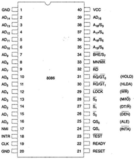
Power supply and frequency signals
It uses 5V DC supply at VCC pin 40, and uses ground at VSS pin 1 and 20 for its operation.
Clock signal
Clock signal is provided through Pin-19. It provides timing to the processor for operations. Its frequency is different for different versions, i.e. 5MHz, 8MHz and 10MHz.
Address/data bus
AD0-AD15. These are 16 address/data bus. AD0-AD7 carries low order byte data and AD8AD15 carries higher order byte data. During the first clock cycle, it carries 16-bit address and after that it carries 16-bit data.
Address/status bus
A16-A19/S3-S6. These are the 4 address/status buses. During the first clock cycle, it carries 4-bit address and later it carries status signals.
S7/BHE
BHE stands for Bus High Enable. It is available at pin 34 and used to indicate the transfer of data using data bus D8-D15. This signal is low during the first clock cycle, thereafter it is active.
Read
It is available at pin 32 and is used to read signal for Read operation.
Ready
It is available at pin 22. It is an acknowledgement signal from I/O devices that data is transferred. It is an active high signal. When it is high, it indicates that the device is ready to transfer data. When it is low, it indicates wait state.
RESET
It is available at pin 21 and is used to restart the execution. It causes the processor to immediately terminate its present activity. This signal is active high for the first 4 clock cycles to RESET the microprocessor.
INTR
It is available at pin 18. It is an interrupt request signal, which is sampled during the last clock cycle of each instruction to determine if the processor considered this as an interrupt or not.
NMI
It stands for non-maskable interrupt and is available at pin 17. It is an edge triggered input, which causes an interrupt request to the microprocessor.
This signal is like wait state and is available at pin 23. When this signal is high, then the processor has to wait for IDLE state, else the execution continues.
MN/MX
It stands for Minimum/Maximum and is available at pin 33. It indicates what mode the processor is to operate in; when it is high, it works in the minimum mode and vice-versa.
INTA
It is an interrupt acknowledgement signal and id available at pin 24. When the microprocessor receives this signal, it acknowledges the interrupt.
ALE
It stands for address enable latch and is available at pin 25. A positive pulse is generated each time the processor begins any operation. This signal indicates the availability of a valid address on the address/data lines.
DEN
It stands for Data Enable and is available at pin 26. It is used to enable Trans receiver 8286. The trans receiver is a device used to separate data from the address/data bus.
DT/R
It stands for Data Transmit/Receive signal and is available at pin 27. It decides the direction of data flow through the transreceiver. When it is high, data is transmitted out and vice-a-versa.
M/IO
This signal is used to distinguish between memory and I/O operations. When it is high, it indicates I/O operation and when it is low indicates the memory operation. It is available at pin 28.
WR
It stands for write signal and is available at pin 29. It is used to write the data into the memory or the output device depending on the status of M/IO signal.
HLDA
It stands for Hold Acknowledgement signal and is available at pin 30. This signal acknowledges the HOLD signal.
HOLD
This signal indicates to the processor that external devices are requesting to access the address/data buses. It is available at pin 31.
QS1 and QS0
These are queue status signals and are available at pin 24 and 25. These signals provide the status of instruction queue. Their conditions are shown in the following table −
QS0 | QS1 | Status |
0 | 0 | No operation |
0 | 1 | First byte of opcode from the queue |
1 | 0 | Empty the queue |
1 | 1 | Subsequent byte from the queue |
S0, S1, S2
These are the status signals that provide the status of operation, which is used by the Bus Controller 8288 to generate memory & I/O control signals. These are available at pin 26, 27, and 28. Following is the table showing their status −
S2 | S1 | S0 | Status |
0 | 0 | 0 | Interrupt acknowledgement |
0 | 0 | 1 | I/O Read |
0 | 1 | 0 | I/O Write |
0 | 1 | 1 | Halt |
1 | 0 | 0 | Opcode fetch |
1 | 0 | 1 | Memory read |
1 | 1 | 0 | Memory write |
1 | 1 | 1 | Passive |
LOCK
When this signal is active, it indicates to the other processors not to ask the CPU to leave the system bus. It is activated using the LOCK prefix on any instruction and is available at pin 29.
RQ/GT1 and RQ/GT0
These are the Request/Grant signals used by the other processors requesting the CPU to release the system bus. When the signal is received by CPU, then it sends acknowledgment. RQ/GT0 has a higher priority than RQ/GT1.
Minimum mode | Maximum mode |
In minimum mode there can be only one processor i.e. 8086. | In maximum mode there can be multiple processors with 8086, like 8087 and 8089. |
MN/MX¯ is 1 to indicate minimum mode. | MN/MX¯is 0 to indicate maximum mode. |
ALE for the latch is given by 8086 as it is the only processor in the circuit. | ALE for the latch is given by 8288 bus controller as there can be multiple processors in the circuit. |
DEN¯and DT/R¯T/R¯ for the trans-receivers are given by 8086 itself. | DT/R¯¯for the trans-receivers are given by 8288 bus controller. |
HOLD and HLDA signals are used for bus request with a DMA controller like 8237. | RQ¯/GT¯Q¯/GT¯,lines are used for bus requests by other processors like 8087 or 8089. |
The circuit is simpler. | The circuit is more complex. |
Multiprocessing cannot be performed hence performance is lower. | As multiprocessing can be performed, it can give very high performance. |
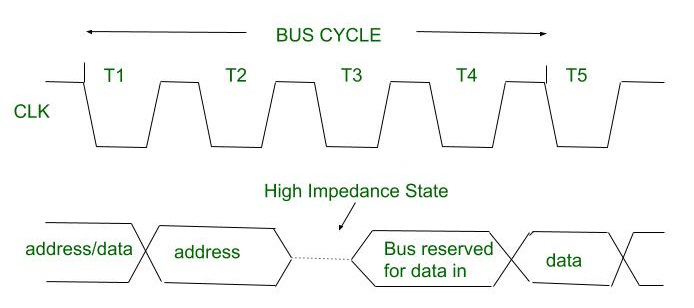
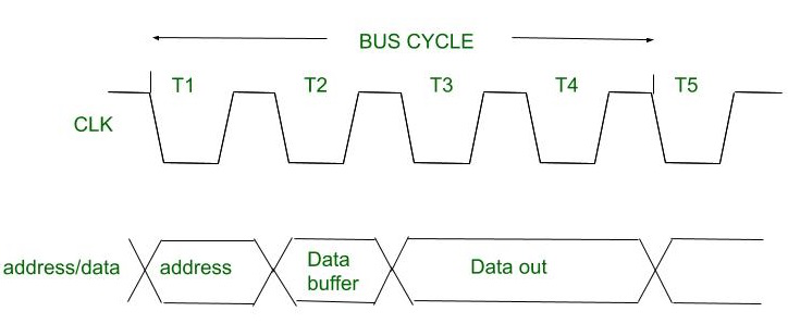
There are at least four clock periods in a bus cycle of 8086 microprocessor. These four clock periods are called T1, T2, T3 and T4 states.
These four clock states gives bus cycle duration T of 200 ns *4 = 800 ns in 5-MHz 8086 system.
- Read Cycle :
When a read cycle is to be performed, during T1 microprocessor puts an address on address bus, and then bus is put in high impedance state during T2 state. Data to be read must be out on bus during T3 and T4. During T3 bus is made “reserved for data in” and finally data is read during T4.
2. Write Cycle :
In case of write memory cycle, during T1 state microprocessor puts an address on address bus. Data is put on data bus by CPU during T2 state and maintained during T3 and T4 states, that is written out to memory or I/O devices.
8086 is 16-bit processor that can supports 1Mbyte (i.e. 20-bit address bus: 220) of external memory over the address range 0000016 to FFFFF16. The 8086 organizes memory as individual bytes of data. The 8086 can access any two consecutive bytes as a word of data. The lower-addressed byte is the least significant byte of the word, and the higher- addressed byte is its most significant byte.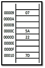
Part of 1 Mbyte Memory
The above figure represents:
Storage location of address 0000916 contains the value 716, while the location of address 0001016 contains the value 7D16.
The 16-bit word 225A16is stored in the locations 0000C16 to 0000D16
The word of data is at an even-address boundary (i.e. address of least significant byte is even) is called aligned word.
The word of data is at an odd-address boundary is called misaligned word, as shown in Figure below.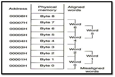
Figure: Aligned and misaligned word
To store double word four locations are needed. The double word that it’s least significant byte address is a multiple of 4 (e.g. 0 16, 416, 816 ...) is called aligned double word. The double word at address of non-multiples of 4 is called misaligned double word shown in Figure below.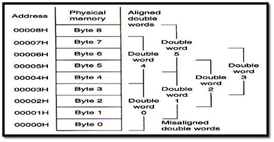
Figure: Aligned and misaligned double word
Memory segmentation
The size of address bus of 8086 is 20 and is able to address 1 Mbytes ( ) of physical memory, but all this memory is not active at one time. Actually, this 1Mbytes of memory are partitioned into 16 parts named as segments. Size of the each segment is 64Kbytes (65,536).
Only four of these segments are active at a time:
- Code segment holds the program instruction codes
- Stack segment is used to store interrupt and subroutine return addresses
- Data segment stores data for the program
- Extra segment is an extra data segment (often used for shared data)
- Each of these segments are addressed by an address stored in corresponding segment registers: CS(code segment), SS(stack segment), DS(data segment), and ES(extra segment). These registers contain a 16-bit base address that points to the lowest addressed byte of the segment. Because the segment registers cannot store 20 bits, they only store the upper 16 bits. The BIU takes care of this problem by appending four 0's to the low-order bits of the segment register. In effect, this multiplies the segment register contents by 16.
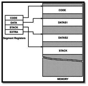
The segment registers are user accessible, which means that the programmer can change the content of segment registers through software.
Programming model:
How can a 20-bit address be obtained, if there are only 16-bit registers?
However, the largest register is only 16 bits (64k); so physical addresses have to be calculated. These calculations are done in hardware within the microprocessor.
The 16-bit contents of segment register gives the starting/ base address of particular segment. To address a specific memory location within a segment we need an offset address. The offset address is also 16-bit wide and it is provided by one of the associated pointer or index register.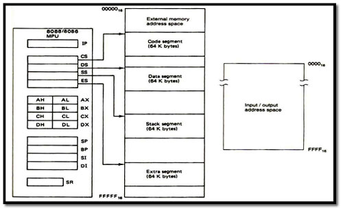
Figure: Software model of 8086 microprocessor
The above figure illustrates the software architecture of the 8086 microprocessor. From this diagram, we see that it includes fourteenl6-bit internal registers: the instruction pointer (IP), four data registers (AX, BX, CX, and DX), two pointer registers (BP and SP), two index registers (SI and DI), four segment registers (CS, DS, SS, and ES) and status register (SR), with nine of its bits implemented as status and control flags.
c) Logical and Physical Address
Addresses within a segment can range from address 00000h to address 0FFFFh. This corresponds to the 64K-bytelength of the segment. An address within a segment is called an offset or logical address.
A logical address gives the displacement from the base address of the segment to the desired location within it, as opposed to its "real" address, which maps directly anywhere into the 1 MByte memory space. This "real" address is called the physical address.
What is the difference between the physical and the logical address?
The physical address is 20 bits long and corresponds to the actual binary code output by the BIU on the address bus lines. The logical address is an offset from location 0 of a given segment.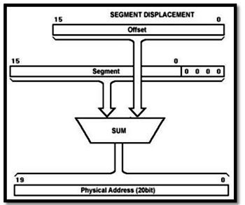 .
.
To specify the logical address XXXX in the stack segment, use the convention SS:XXXX, which is equal to [SS] * 16 + XXXX.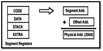
Logical address is in the form of: Base Address: Offset
Offset is the displacement of the memory location from the starting location of the segment.
To calculate the physical address of the memory, BIU uses the following formula:
Physical Address = Base Address of Segment * 16 + Offset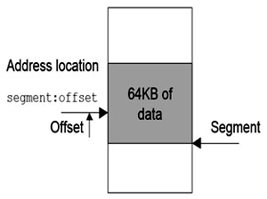
Example:
The value of Data Segment Register (DS) is 2222H.
To convert this 16-bit address into 20-bit, the BIU appends 0H to the LSB (by multiplying with 16) of the address. After appending, the starting address of the Data Segment becomes 22220H.
Data at any location has a logical address specified as:2222H: 0016H
Where 0016H is the offset, 2222 H is the value of DS
Therefore the physical address:22220H + 0016H
: 22236 H
There are four common types of memory:
• Read only memory ( ROM )
• Flash memory ( EEPROM )
• Static Random access memory ( SARAM )
• Dynamic Random access memory ( DRAM ).
• Pin connections common to all memory devices are:
The address input, data output or input/outputs, selection input and control input used to select a read or write operation.
• Address connections: All memory devices have address inputs that select a memory location within the memory device. Address inputs are labeled from A0 to An.
• Data connections: All memory devices have a set of data outputs or input/outputs. Today many of them have bi-directional common I/O pins.
• Selection connections: Each memory device has an input, that selects or enables the memory device. This kind of input is most often called a chip select ( CS ), chip enable ( CE ) or simply select ( S ) input.
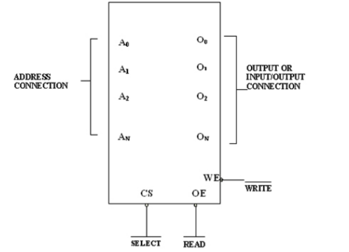
RAM memory generally has at least one CS or S input and ROM at least one CE . • If the CE , CS , S input is active the memory device perform the read or write. • If it is inactive the memory device cannot perform read or write operation. • If more than one CS connection is present, all are active to perform read or write data.
Types of addressing modes:
Register mode – In this type of addressing mode both the operands are registers.
Example:
MOV AX, BX
XOR AX, DX
ADD AL, BL
Immediate mode – In this type of addressing mode the source operand is a 8 bit or 16 bit data. Destination operand can never be immediate data.
Example:
MOV AX, 2000
MOV CL, 0A
ADD AL, 45
AND AX, 0000
MOV AX, 2000
MOV CS, AX
Displacement or direct mode – In this type of addressing mode the effective address is directly given in the instruction as displacement.
Example:
MOV AX, [DISP]
MOV AX, [0500]
Register indirect mode – In this addressing mode the effective address is in SI, DI or BX.
Example:
MOV AX, [DI]
ADD AL, [BX]
MOV AX, [SI]
Based indexed mode – In this the effective address is sum of base register and index register.
Base register: BX, BP
Index register: SI, DI
The physical memory address is calculated according to the base register.
Example:
MOV AL, [BP+SI]
MOV AX, [BX+DI]
Indexed mode – In this type of addressing mode the effective address is sum of index register and displacement.
Example:
MOV AX, [SI+2000]
MOV AL, [DI+3000]
Based mode – In this the effective address is the sum of base register and displacement.
Example:
MOV AL, [BP+ 0100]
Based indexed displacement mode – In this type of addressing mode the effective address is the sum of index register, base register and displacement.
Example:
MOV AL, [SI+BP+2000]
String mode – This addressing mode is related to string instructions. In this the value of SI and DI are auto incremented and decremented depending upon the value of directional flag.
Example:
MOVS B
MOVS W
Input/Output mode – This addressing mode is related with input output operations.
Example:
IN A, 45
OUT A, 50
Relative mode –
In this the effective address is calculated with reference to instruction pointer.
Example:
JNZ 8 bit address
IP=IP+8 bit address
DB (DEFINE BYTE)
The DB directive is used to declare a byte type variable, or a set aside one or more storage locations of type byte in memory.
PRICES DB 49H, 98H, 29H;Declare array of 3 bytes named PRICES and initialize them with specified values.
DD (DEFINE DOUBLE WORD)
The DD directive is used to declare a variable of type double word or to reserve memory locations, which can be accessed as type double word.
Example:
ARRAY DD 25629261H
This will define a double word named ARRAY and initialize the double word with the specified value when the program is loaded into memory to be run. The low word, 9261H, will be put in memory at a lower address than the high word.
DQ (DEFINE QUADWORD)
The DQ directive is used to tell the assembler to declare a variable 4 words in length or to reserve 4 words of storage in memory.
Example:
BIG_NUMBER DQ 243598740192A92BH
This will declare a variable named BIG_NUMBER and initialize the 4 words set aside with the specified number when the program is loaded into memory to be run.
DT (DEFINE TEN BYTES)
The DT directive is used to tell the assembler to declare a variable, which is 10 bytes in length or to reserve 10 bytes of storage in memory.
Example:
PACKED_BCD DT 11223344556677889900
This will declare an array named PACKED_BCD, which is 10 bytes in length. It will initialize the 10 bytes with the values 11, 22, 33, 44, 55, 66, 77, 88, 99, and 00 when the program is loaded into memory to be run. The statement RESULT DT 20H DUP (0) will declare an array of 20H blocks of 10 bytes each and initialize all 320 bytes to 00 when the program is loaded into memory to be run.
DW (DEFINE WORD)
The DW directive is used to tell the assembler to define a variable of type word or to reserve storage locations of type word in memory. The statement MULTIPLIER DW 437AH, for example, declares a variable of type word named MULTIPLIER, and initialized with the value 437AH when the program is loaded into memory to be run.
Example:
WORDS DW 1234H, 3456H; Declares an array of 2 words and initialize them with the specified values.
STORAGE DW 100 DUP (0); Reserve an array of 100 words of memory and initialize all 100 words with 0000. Array is named as STORAGE.
STORAGE DW 100 DUP (?); Reserve 100 word of storage in memory and give it the name STORAGE, but leave the words un-initialized.
Segment:
The SEGMENT directive is used to indicate the start of a logical segment. Preceding the SEGMENT directive is the name you want to give the segment.
For example, the statement CODE SEGMENT indicates to the assembler the start of a logical segment called CODE. The SEGMENT and ENDS directive are used to “bracket” a logical segment containing code of data.
Data Transfer instruction
All the instructions which perform data movement come under this category. The source data may be a register, memory location, port etc. the destination may be a register, memory location or port. The following instructions come under this category:
Instruction | Description |
MOV | Moves data from register to register, register to memory, Memory to register, memory to accumulator, Accumulator to memory, etc. |
LDS | Loads a word from the specified memory locations Into specified register. It also loads a word from the next Two memory locations into DS register. |
LES | Loads a word from the specified memory locations into The specified register. It also loads a word from next Two memory locations into ES register. |
LEA | Loads offset address into the specified register. |
LAHF | Loads low order 8-bits of the flag register into AH register. |
SAHF | Stores the content of AH register into low order bits of the Flags register. |
XLAT/XLATB | Reads a byte from the lookup table. |
XCHG | Exchanges the contents of the 16-bit or 8-bit specified Register with the contents of AX register, Specified register or memory locations. |
PUSH | Pushes (sends, writes or moves) the content of a Specified register or memory location(s) onto The top of the stack. |
POP | Pops (reads) two bytes from the top of the stack And keeps them in a specified register, or memory location(s). |
POPF | Pops (reads) two bytes from the top of the stack and Keeps them in the flag register. |
IN | Transfers data from a port to the accumulator or AX, DX or AL register. |
OUT | Transfers data from accumulator or AL or AX register to an I/O port identified by the Second byte of the instruction. |
Arithmetic Instructions
Instructions of this group perform addition, subtraction, multiplication, division, increment, decrement, comparison, ASCII and decimal adjustment etc.
The following instructions come under this category:
Instruction | Description |
ADD | Adds data to the accumulator i.e. AL or AX register or memory locations. |
ADC | Adds specified operands and the carry status (i.e. carry of the previous stage). |
SUB | Subtract immediate data from accumulator, memory or register. |
SBB | Subtract immediate data with borrow from accumulator, Memory or register. |
MUL | Unsigned 8-bit or 16-bit multiplication. |
IMUL | Signed 8-bit or 16-bit multiplication. |
DIV | Unsigned 8-bit or 16-bit division. |
IDIV | Signed 8-bit or 16-bit division. |
INC | Increment Register or memory by 1. |
DEC | Decrement register or memory by 1. |
DAA | Decimal Adjust after BCD Addition: When two BCD numbers are added, the DAA is used after ADD or ADC instruction to get correct answer in BCD. |
DAS | Decimal Adjust after BCD Subtraction: When two BCD numbers are added, the DAS is used after SUB Or SBB instruction to get correct answer in BCD. |
AAA | ASCII Adjust for Addition: When ASCII codes of two decimal Digits are added, the AAA is used after addition to get correct answer In unpacked BCD. |
AAD | Adjust AX Register for Division: It converts two unpacked BCD digits In AX to the equivalent binary number. This adjustment is done before dividing two unpacked BCD digits In AX by an unpacked BCD byte. |
AAM | Adjust result of BCD Multiplication: This instruction is used After the multiplication of two unpacked BCD. |
AAS | ASCII Adjust for Subtraction: This instruction is used to get The correct result in unpacked BCD after the subtraction of The ASCII code of a number from ASCII code another number. |
CBW | Convert signed Byte to signed Word. |
CWD | Convert signed Word to signed Doubleword. |
NEG | Obtains 2's complement (i.e. negative) of the content of an 8-bit Or 16-bit specified register or memory location(s). |
CMP | Compare Immediate data, register or memory with accumulator , register or memory location(s). |
Logical Instructions
Instruction of this group perform logical AND, OR, XOR, NOT and TEST operations. The following instructions come under this category:
Instruction | Description |
AND | Performs bit by bit logical AND operation of two operands And places the result in the specified destination. |
OR | Performs bit by bit logical OR operation of two operands And places the result in the specified destination. |
XOR | Performs bit by bit logical XOR operation of two operands And places the result in the specified destination. |
NOT | Takes one's complement of the content of a specified register Or memory location(s). |
TEST | Perform logical AND operation of a specified operand with Another specified operand. |
Rotate Instructions
The following instructions come under this category:
Instruction | Description |
RCL | Rotate all bits of the operand left by Specified number of bits through carry flag. |
RCR | Rotate all bits of the operand right by Specified number of bits through carry flag. |
ROL | Rotate all bits of the operand left By specified number of bits. |
ROR | Rotate all bits of the operand right By specified number of bits. |
Shift Instructions
The following instructions come under this category:
Instruction | Description |
SAL or SHL | Shifts each bit of operand left by specified number Of bits and put zero in LSB position. |
SAR | Shift each bit of any operand right by specified Number of bits. Copy old MSB into new MSB. |
SHR | Shift each bit of operand right by Specified number Of bits and put zero in MSB position. |
Branch Instructions
It is also called program execution transfer instruction. Instructions of this group transfer program execution from the normal sequence of instructions to the specified destination or target. The following instructions come under this category:
Instruction | Description |
JA or JNBE | Jump if above, not below, or equal i.e. When CF and ZF = 0 |
JAE/JNB/JNC | Jump if above, not below, equal or no carry i.e. When CF = 0 |
JB/JNAE/JC | Jump if below, not above, equal or carry i.e. when CF = 0 |
JBE/JNA | Jump if below, not above, or equal i.e. When CF and ZF = 1 |
JCXZ | Jump if CX register = 0 |
JE/JZ | Jump if zero or equal i.e. when ZF = 1 |
JG/JNLE | Jump if greater, not less or equal i.e. When ZF = 0 and CF = OF |
JGE/JNL | Jump if greater, not less or equal i.e. when SF = OF |
JL/JNGE | Jump if less, not greater than or equal i.e. when SF ≠ OF |
JLE/JNG | Jump if less, equal or not greater i.e. When ZF = 1 and SF ≠ OF |
JMP | Causes the program execution to jump Unconditionally to the memory address Or label given in the instruction. |
CALL | Calls a procedure whose address Is given in the instruction and saves Their return address to the stack. |
RET | Returns program execution from a Procedure (subroutine) to the next instruction Or main program. |
IRET | Returns program execution from An interrupt service procedure (subroutine) to the main program. |
INT | Used to generate software interrupt
At the desired point in a program. |
INTO | Software interrupts to indicate overflow after arithmetic operation. |
LOOP | Jump to defined label until CX = 0. |
LOOPZ/LOOPE | Decrement CX register and Jump if CX ≠ 0 and ZF = 1. |
LOOPNZ/LOOPNE | Decrement CX register and Jump if CX ≠ 0 and ZF = 0. |
Here, CF = Carry Flag
ZF = Zero Flag
OF = Overflow Flag
SF = Sign Flag
CX = Register
Flag Manipulation and Processor Control Instructions
Instructions of this instruction set are related to flag manipulation and machine control. The following instructions come under this category:
Instruction | Description |
CLC | Clear Carry Flag: This instruction resets the carry flag CF to 0. |
CLD | Clear Direction Flag: This instruction resets the direction flag DF to 0. |
CLI | Clear Interrupt Flag: This instruction resets the interrupt flag IF to 0. |
CMC | This instruction take complement of carry flag CF. |
STC | Set carry flag CF to 1. |
STD | Set direction flag to 1. |
STI | Set interrupt flag IF to 1. |
HLT | Halt processing. It stops program execution. |
NOP | Performs no operation. |
ESC | Escape: makes bus free for external master like a coprocessor or peripheral device. |
WAIT | When WAIT instruction is executed, the processor enters An idle state in which the processor does no processing. |
LOCK | It is a prefix instruction. It makes the LOCK pin Low till the execution of the next instruction. |
String Instructions
String is series of bytes or series of words stored in sequential memory locations. The 8086 provides some instructions which handle string operations such as string movement, comparison, scan, load and store.
The following instructions come under this category:
Instruction | Description |
MOVS/MOVSB/MOVSW | Moves 8-bit or 16-bit data from the memory Location(s) addressed by SI register To the memory location addressed By DI register. |
CMPS/CMPSB/CMPSW | Compares the content of memory location Addressed by DI register with the content of Memory location addressed by SI register. |
SCAS/SCASB/SCASW | Compares the content of accumulator with the content Of memory location addressed by DI register in The extra segment ES. |
LODS/LODSB/LODSW | Loads 8-bit or 16-bit data from Memory location addressed By SI register into AL or AX register. |
STOS/STOSB/STOSW | Stores 8-bit or 16-bit data from AL or AX register in the Memory location addressed by DI register. |
REP | Repeats the given instruction until CX ≠ 0 |
REPE/ REPZ | Repeats the given instruction till CX ≠ 0 and ZF = 1 |
REPNE/REPNZ | Repeats the given instruction till CX ≠ 0 and ZF = 0 |
1.ALP for Finding Factorial of number using procedures
CODE SEGMENT
ASSUME CS:CODE
START: MOV AX,7
CALL FACT
MOV AH,4CH
INT 21H
FACT PROC NEAR
MOV BX,AX
DEC BX
BACK: MUL BX
DEC BX
JNZ BACK
RET
ENDP
CODE ENDS
END START
2.Addition
ORG0000h
MOV DX, #07H // move the value 7 to the register AX//
MOV AX, #09H // move the value 9 to accumulator AX//
Add AX, 00H // add CX value with R0 value and stores the result in AX//
END
3.Multiplication
ORG0000h
MOV DX, #04H // move the value 4 to the register DX//
MOV AX, #08H // move the value 8 to accumulator AX//
MUL AX, 06H // Multiplied result is stored in the Accumulator AX //
END
4.Subtraction
ORG 0000h
MOV DX, #02H // move the value 2 to register DX//
MOV AX, #08H // move the value 8 to accumulator AX//
SUBB AX, 09H // Result value is stored in the Accumulator A X//
END
5. Division
ORG 0000h
MOV DX, #08H // move the value 3 to register DX//
MOV AX, #19H // move the value 5 to accumulator AX//
DIV AX, 08H // final value is stored in the Accumulator AX //
END
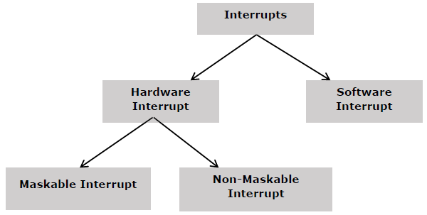
The following image shows the types of interrupts we have in a 8086 microprocessor −
Hardware Interrupts
Hardware interrupt is caused by any peripheral device by sending a signal through a specified pin to the microprocessor.
The 8086 has two hardware interrupt pins, i.e. NMI and INTR. NMI is a non-maskable interrupt and INTR is a maskable interrupt having lower priority. One more interrupt pin associated is INTA called interrupt acknowledge.
NMI
It is a single non-maskable interrupt pin (NMI) having higher priority than the maskable interrupt request pin (INTR)and it is of type 2 interrupt.
When this interrupt is activated, these actions take place −
- Completes the current instruction that is in progress.
- Pushes the Flag register values on to the stack.
- Pushes the CS (code segment) value and IP (instruction pointer) value of the return address on to the stack.
- IP is loaded from the contents of the word location 00008H.
- CS is loaded from the contents of the next word location 0000AH.
- Interrupt flag and trap flag are reset to 0.
INTR
The INTR is a maskable interrupt because the microprocessor will be interrupted only if interrupts are enabled using set interrupt flag instruction. It should not be enabled using clear interrupt Flag instruction.
The INTR interrupt is activated by an I/O port. If the interrupt is enabled and NMI is disabled, then the microprocessor first completes the current execution and sends ‘0’ on INTA pin twice. The first ‘0’ means INTA informs the external device to get ready and during the second ‘0’ the microprocessor receives the 8 bit, say X, from the programmable interrupt controller.
These actions are taken by the microprocessor −
- First completes the current instruction.
- Activates INTA output and receives the interrupt type, say X.
- Flag register value, CS value of the return address and IP value of the return address are pushed on to the stack.
- IP value is loaded from the contents of word location X × 4
- CS is loaded from the contents of the next word location.
- Interrupt flag and trap flag is reset to 0
Software Interrupts
Some instructions are inserted at the desired position into the program to create interrupts. These interrupt instructions can be used to test the working of various interrupt handlers. It includes −
INT- Interrupt instruction with type number
It is 2-byte instruction. First byte provides the op-code and the second byte provides the interrupt type number. There are 256 interrupt types under this group.
Its execution includes the following steps −
- Flag register value is pushed on to the stack.
- CS value of the return address and IP value of the return address are pushed on to the stack.
- IP is loaded from the contents of the word location ‘type number’ × 4
- CS is loaded from the contents of the next word location.
- Interrupt Flag and Trap Flag are reset to 0
The starting address for type0 interrupt is 000000H, for type1 interrupt is 00004H similarly for type2 is 00008H and ……so on. The first five pointers are dedicated interrupt pointers. i.e. −
- TYPE 0 interrupt represents division by zero situation.
- TYPE 1 interrupt represents single-step execution during the debugging of a program.
- TYPE 2 interrupt represents non-maskable NMI interrupt.
- TYPE 3 interrupt represents break-point interrupt.
- TYPE 4 interrupt represents overflow interrupt.
The interrupts from Type 5 to Type 31 are reserved for other advanced microprocessors, and interrupts from 32 to Type 255 are available for hardware and software interrupts.
INT 3-Break Point Interrupt Instruction
It is a 1-byte instruction having op-code is CCH. These instructions are inserted into the program so that when the processor reaches there, then it stops the normal execution of program and follows the break-point procedure.
Its execution includes the following steps −
- Flag register value is pushed on to the stack.
- CS value of the return address and IP value of the return address are pushed on to the stack.
- IP is loaded from the contents of the word location 3×4 = 0000CH
- CS is loaded from the contents of the next word location.
- Interrupt Flag and Trap Flag are reset to 0
INTO - Interrupt on overflow instruction
It is a 1-byte instruction and their mnemonic INTO. The op-code for this instruction is CEH. As the name suggests it is a conditional interrupt instruction, i.e. it is active only when the overflow flag is set to 1 and branches to the interrupt handler whose interrupt type number is 4. If the overflow flag is reset then, the execution continues to the next instruction.
Its execution includes the following steps −
- Flag register values are pushed on to the stack.
- CS value of the return address and IP value of the return address are pushed on to the stack.
- IP is loaded from the contents of word location 4×4 = 00010H
- CS is loaded from the contents of the next word location.
- Interrupt flag and Trap flag are reset to 0
The figure below shows the architectural representation of 80286 microprocessor:
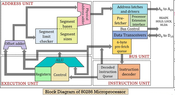
It is a 16-bit microprocessor thus holds a 16-bit data bus and 24-bit address bus. Also, unlike the 8086 microprocessors, it offers non-multiplexed address and data bus, which increases the operating speed of the system.
80286 is composed of nearly around 125K transistors and the pin configuration has a total of 68 pins.
The CPU, central processing unit of 80286 microprocessor, consists of 4 functional block:
- Address Unit
- Bus Unit
- Instruction Unit
- Execution Unit
Firstly, the physical address from where the data or instruction is to be fetched is calculated, by the address unit. Once the physical address is calculated then the calculated address is handed over to the bus unit.
More specifically we can say, that the calculated address is loaded on the address bus of the bus unit.
This address specifies the memory location from where the data or instruction is to be fetched. The fetching of data through the memory is done through the data bus. For faster execution of instruction, the BU fetches the instructions in advanced from the memory and stores them in the queue.
This is done through the bus control module. The prefetched instructions are stored in a 6-byte instruction queue. This instruction queue then further sends the instruction to the instruction unit.
The instruction unit on receiving the instructions now starts decoding the instruction. As instructions are stored in prefetched queue thus the decoder continuously decodes the fetched instructions and stores them into decoded instruction queue.
Now after the instructions gets decoded then further these are needed to be executed. So, the instructions from decoded instruction queue are fed to the execution unit.
The main component of EU is ALU i.e., arithmetic and logic unit that performs the arithmetic and logic operations over the operand according to the decoded instruction.
Once the execution of the instruction is performed then the result of the operation i.e., the desired data is send to the register bank through the data bus.
80286 is just a modified version of 8086. The register set in 80286 is same as that of 8086 microprocessor.
- It holds 8 general purpose registers of 16 bit each.
- It contains 4 segment register each of 16-bit.
- Also has status and control register and instruction pointer.
Interrupt of 80286 Microprocessor
We know that whenever an interrupt gets generated in a system, then the execution of the current program is stopped and the execution gets transferred to the new program location where the interrupt is generated.
But once the interrupt gets executed then then in order to get back to the original program, its address as well as machine state must be stored in the stack. Basically there exist 3 categories of interrupt in 80286 microprocessor:
- External interrupt (Hardware interrupt)
- INT instruction interrupt (Software interrupt)
- Internally generated interrupt due to some exceptions
External or hardware initiate interrupt are those interrupts that gets generated due to an external input. And are basically of two types:
- Maskable interrupt
- Non-maskable interrupt
Sometimes when multiple programs are allowed to be executed in a system, then this leads to generation of INT instruction, and such an interrupt is known as software interrupt.
Another interrupt in 80286 exist due to some unusual conditions or situations generated in the system that leads to prevention of further execution of the current instruction.
80386
The figure below shows the architectural representation of 80386 microprocessor:
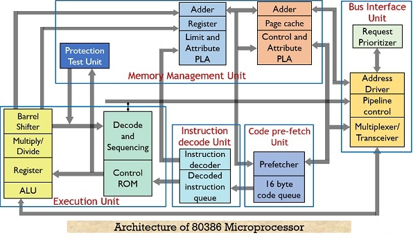
Basically it has 6 functional units which are as follows:
- Bus Interface Unit
- Code Fetch Unit
- Instruction Decode Unit
- Execution Unit
- Memory Management Unit
As we have already discussed that the 80386 possess the ability of 3 stage pipelining thus performs fetching, decoding and execution simultaneously along with memory management and bus accessing. Thus all these units operate parallely.
This pipelining technique leads to reduction in overall processing time thereby increasing the performance of the overall system.
Let us now move further and understand the operation of each unit in detail.
1. Bus Interface Unit
The bus interface unit or BIU holds a 32-bit bidirectional data bus as well as 32-bit address bus. Whenever a need for an instruction or a data fetch is generated by the system then the BIU generates signals (according to the priority) for activating the data and address bus in order to fetch the data from the desired address.
The BIU connects the peripheral devices through the memory unit and also controls the interfacing of external buses with the coprocessors.
2. Code Prefetch Unit
This unit fetches the instructions stored in the memory by making use of system buses. Whenever the system generates a need for an instruction then the code prefetch unit fetches that instruction from the memory and stores it in 16-byte prefetch queue.
So to speed up the operation this unit fetches the instructions in advance and the queue stores these instructions.
The sequence in which the instructions are fetched and gets stored in the queue depends on the order they exist in the memory.
As this unit fetches one double word in single access. So, in such a case, it is not necessary that each time only a single instruction will be fetched, as the fetched instruction can be parts of two different instructions.
It is to be noted here that, code prefetching holds lower priority than data transferring. As whenever, a need for data transfer is generated by the system then immediately the code prefetcher leaves the control over the buses. So that the BIU can transfer the required data.
But prefetching of instruction and storing it in the queue reduces the wait for the upcoming instruction to almost zero.
3. Instruction Decode Unit
We know that instructions in the memory are stored in the form of bits. So, this unit decodes the instructions stored in the prefetch queue. Basically the decoder changes the machine language code into assembly language and transfers it to the processor for further execution.
4. Execution Unit
The decoded instructions are stored in the decoded instruction queue. So, these instructions are provided to the execution unit in order to execute the instructions.
The execution unit controls the execution of the decoded instructions. This unit has a 32-bit ALU, that performs the operation over 32-bit data in one cycle. Also, it consists of 8 general purpose as well as 8 special purpose registers. These are used for data handling and calculation of offset address.
5. Memory Management Unit
This unit has two separate units within it. These are
- Segmentation Unit and
- Paging Unit
Segmentation unit: The segmentation unit plays a vital role in the 80836 microprocessor. It offers protection mechanism in order to protect the code or data present in the memory from application programs.
It gives 4 level protection to the data or code present in the memory. Every information in the memory is assigned a privilege level from PL0 to PL3. Here, PL0 holds the highest priority and PL3 holds the lowest priority.
Suppose a file (either data or code) is needed to be accessed is stored in the memory at PL0. Then only those programs which are working at PL0 would be able to access that file. While other programs will not be able to access the same.
Also, if a file is present at PL1, then programs of PL0 and PL1 both can access it. As PL0 has higher priority than PL1. So, for protection purpose the main part of OS is stored in PL0 while PL3 holds the user programs.
Providing protection to the data or code inside the system is the most advantageous factor that was first given by 80386 microprocessor.
Paging Unit: The paging unit operates only in protected mode and it changes the linear address into physical address. As the programmer only provides the virtual address and not the physical address.
The segmentation unit controls the action of paging unit, as the segmentation unit has the ability to convert logical address into linear address at the time of executing an instruction.
Basically it changes the overall task map into pages and each page has a size of 4K. This allows the handling of task in the form of pages rather than segments.
Paging unit supports multitasking. This is so because the physical memory is not required to hold the whole segment of any task. Despite, only that part of the segment which is needed to be currently executed must be stored in that memory whose physical address is calculated by the paging unit.
This resultantly reduces the memory requirement and hence this frees the memory for other tasks. Thus,we get an effective way for managing the memory to support multitasking.
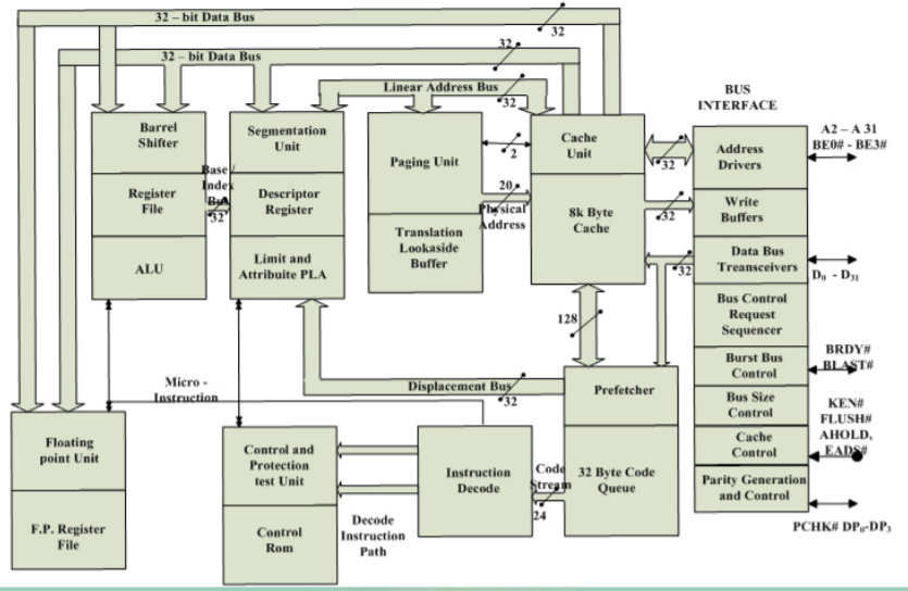
80486
The 32-bit 80486 is the next evolutionary step up from the 80386.
•One of the most obvious feature included in a 80486 is a built in math coprocessor.
This coprocessor is essentially the same as the 80387 processor used with a 80386, but being integrated on the chip allows it to execute math instructions about three times as fast as a 80386/387 combination.
•80486 is an 8Kbyte code and data cache.
•To make room for the additional signals, the 80486 is packaged in a 168 pin, pin grid array package instead of the 132 pin PGA used for the 80386.
Pin Definitions
•A 31-A2 : Address outputs A31-A2 provide the memory and I/O with the address during normal operation. During a cache line invalidation A31-A4 are used to drive the microprocessor.
•A20M3 : The address bit 20 mask causes the 80486 to wrap its address around from location 000FFFFFH to 00000000H as in 8086. This provides a memory system that functions like the 1M byte real memory system in the 8086 processors.
• ADS : The address data strobe become logic zero to indicate that the address bus contains a valid memory address.
•AHOLD: The address hold input causes the microprocessor to place its address bus connections at their high-impedance state, with the remainder of the buses staying active. It is often used by another bus master to gain access for a cache invalidation cycle.
•BREQ: This bus request output indicates that the 486 has generated an internal bus request.
• BE - BE 3 0 : Byte enable outputs select a bank of the memory system when information is transferred between the microprocessor and its memory and I/O. The BE3 signal enables D31 – D24 , BE2 enables D23-D16, BE1 enables D15 – D8 and BE0 enables D7-D0.
•BLAST: The burst last output shows that the burst bus cycle is complete on the next activation of BRDY# signal.
•BOFF : The Back-off input causes the microprocessor to place its buses at their high impedance state during the next cycle. The microprocessor remains in the bus hold state until the BOFF# pin is placed at a logic 1 level.
•NMI : The non-maskable interrupt input requests a type 2 interrupt.
•BRDY : The burst ready input is used to signal the microprocessor that a burst cycle is complete.
•KEN : The cache enable input causes the current bus to be stored in the internal. •LOCK : The lock output becomes a logic 0 for any instruction that is prefixed with the lock prefix.
•W / R : current bus cycle is either a read or a write.
•IGNNE : The ignore numeric error input causes the coprocessor to ignore floating point error and to continue processing data. The signal does not affect the state of the FERR pin.
•FLUSH : The cache flush input forces the microprocessor to erase the contents of its 8K byte internal cache.
•EADS : The external address strobe input is used with AHOLD to signal that an external address is used to perform a cache invalidation cycle.
•FERR : The floating point error output indicates that the floating point coprocessor has detected an error condition. It is used to maintain compatibility with DOS software.
•BS8 : The bus size 8, input causes the 80486 to structure itself with an 8-bit data bus to access byte-wide memory and I/O components.
•BS16 : The bus size 16, input causes the 80486 to structure itself with an 16-bit data bus to access word-wide memory and I/O components.
•PCHK : The parity check output indicates that a parity error was detected during a read operation on the DP3 – DP0 pin.
•PLOCK : The pseudo-lock output indicates that current operation requires more than one bus cycle to perform.
This signal becomes a logic 0 for arithmetic coprocessor operations that access 64 or 80 bit memory data.
References:
Microprocessor 8086 : Architecture, Programming and Interfacing Book by Mathur Sunil
The Intel Microprocessors Book by Barry B. Brey
Assembly Programming and the 8086 Microprocessor Book by Douglas Jones