Unit 4
Overview of Microcontroller
Intel’s 8051 Microcontroller was a successor to 8048 Microcontroller. Initially 8051 Microcontrollers were developed using N-MOS Technology but the use of battery powered devices and their low power consumption lead to usage of CMOS Technology
Some of the 8051 Microcontrollers are produced by different manufacturers like Atmel (AT89C51, AT89S51), Phillips (S87C654), STC Micro (STC89C52), Infineon (SAB-C515, XC800), Siemens (SAB-C501), Silicon Labs (C8051), NXP (NXP700, NXP900), etc.
Most of the modern 8051 Microcontrollers are Silicon IP Cores (Intellectual Property Cores) but discrete 8051 Microcontroller IC’s are also available. Because of their low power consumption, smaller size, and simple architecture, 8051 IP Cores are used in FPGAs (Field Programmable Gate Array) and SoCs (System on Chip) instead of Advanced ARM Architecture based MCUs.
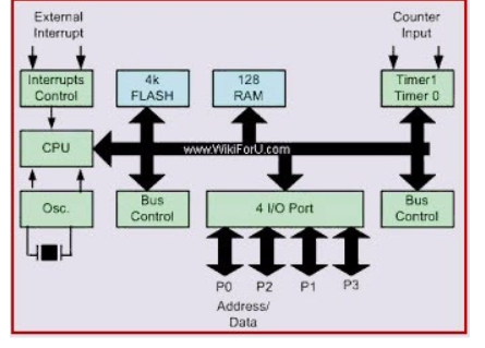
Central Processor Unit (CPU)
CPU is the brain of any processing device of the microcontroller. It monitors and controls all operations that are performed on the Microcontroller units. It reads program written in ROM memory and executes them and does the expected task of that application.
Interrupts
Interrupt is a subroutine call that interrupts the microcontrollers main operations or work and causes it to execute any other program, at the time of operation. An Interrupts gives us a mechanism to put on hold the ongoing operations, execute a subroutine and then again resumes to another type of operations.
Generally, five interrupt sources are there in 8051 Microcontroller.
INTO
- TFO
- INT1
- TF1
- R1/T1
(INT0) ̅ and (INT1) ̅ are external interrupts that could be negative edge triggered or low level triggered. When All these interrupts are activated, set the corresponding flags except for serial interrupt.
The interrupt flags are cleared when the processor branches to the interrupt service routine (ISR). The timers and serial port interrupts are external interrupts.
Memory
The program tells microcontroller to do specific tasks. These programs require a memory where they can be saved and read by Microcontroller to perform specific operations of a task.
The memory which is used to store the program known as code memory or Program memory It is also known as ROM memory.
The data memory of the 8051 is used to store data temporarily for operation is known RAM memory. 8051 microcontroller has 4K of code memory or program memory, that has 4KB ROM and also 128 bytes of data memory of RAM.
BUS
Basically, Bus is a collection of wires which work as a communication channel or medium for transfer of Data. These buses consist of 8, 16 or more wires of the microcontroller. Thus, these can carry 8 bits,16 bits simultaneously. Here two types of buses that are shown in below
- Address Bus
- Data Bus
Address Bus: Microcontroller 8051 has a 16 bit address bus for transferring the data. It is used to address memory locations and to transfer the address from CPU to Memory of the microcontroller. It has four addressing modes that are
- Immediate addressing modes.
- Bank address (or) Register addressing mode.
- Direct Addressing mode.
- Register indirect addressing mode.
Data Bus: Microcontroller 8051 has 8 bits of data bus, which is used to carry data of particular applications.
Oscillator
The 8051 microcontroller has an on-chip oscillator which works as a clock source for Central Processing Unit of the microcontroller. The output pulses of oscillator are stable. Therefore, it enables synchronized work of all parts of the 8051 Microcontroller.
Input/Output Port
Normally microcontroller is used in embedded systems to control the operation of machines in the microcontroller. Therefore, to connect to other machines, devices or peripherals we require I/O interfacing ports in the microcontroller interface. For this purpose, microcontroller 8051 has 4 input, output ports to connect it to the other peripherals
Timers/Counters
8051 microcontroller has two 16-bit timers and counters. These counters are again divided into 8-bit register. The timers are used for measurement of intervals to determine the pulse width of pulses.
The 8051 Microcontroller Memory is separated into Program Memory (ROM) and Data Memory (RAM). The Program Memory of the 8051 Microcontroller is used for storing the program to be executed, which means instructions. The Data Memory is used for storing temporary variable data and intermediate results.
Program Memory (ROM) of 8051
In 8051 Microcontroller, the code or instructions that must be executed are stored in the Program Memory, which is also called as the ROM of the Microcontroller. The original 8051 Microcontroller by Intel has 4KB of internal ROM.
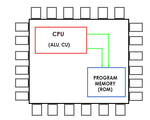
In 4KB of Internal ROM, the address space is 0000H to 0FFFH. If the address space that is the program addresses exceeds this value, then the CPU will automatically fetch the code from the external Program Memory.
For External Access Pin (EA Pin) must be pulled HIGH i.e. when the EA Pin is high, the CPU first fetches instructions from the Internal Program Memory in the address range of 0000H to 0FFFFH and if the memory addresses exceed the limit, then the instructions are fetched from the external ROM in the address range of 1000H to FFFFH.
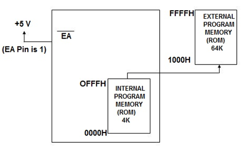
External access
There is also an alternative method to fetch the instructions that is ignore the Internal ROM and fetch all the instructions only from External Program Memory(External ROM).
For this purpose EA pin must be connected to GND . In this case the memory addresses of external ROM will be from 0000H to FFFFH.
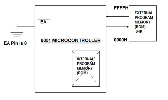
External Program Memory
Data Memory (RAM) of 8051 Microcontroller
- Data Memory or RAM of 8051 Microcontroller stores temporary data and intermediate results that are generated and used during the normal operation of the microcontroller.
- Currently 8051 Microcontroller have 256B of RAM. Of this 256B, the first 128B memory addresses from 00H to 7FH is divided in to Working Registers organized as Register Banks, Bit – Addressable Area and General Purpose RAM known as Scratchpad area.
- In the first 128B of RAM (from 00H to 7FH), the first 32B that is memory from addresses 00H to 1FH consists of 32 Working Registers that are organized as four banks with 8 Registers in each Bank.
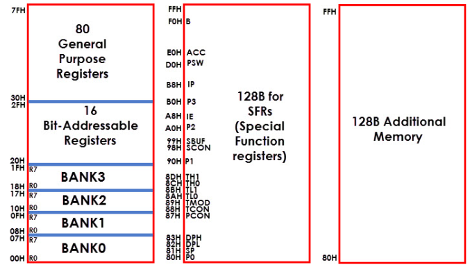
Lower 128B(00H to 07H) Upper 128B(80H-FFH)
(Direct and Indirect Addressing) (Direct Addressing) (Indirect Addressing)
- The 4 banks are named as Bank0, Bank1, Bank2 and Bank3. Each Bank consists of 8 registers named as R0 – R7. Each Register can be addressed in two ways: by name or by address.
- To address the register by name, first the corresponding Bank must be selected. In order to select the bank, use RS0 and RS1 bits of the Program Status Word (PSW) Register (RS0 and RS1 are 3rd and 4th bits in the PSW Register).
- When addressing the Register using its address say 12H for example, the corresponding Bank may or may not be selected. (12H corresponds to R2 in Bank2).
- The next 16B of the RAM i.e. from 20H to 2FH are Bit – Addressable memory locations. There are totally 128 bits that can be addressed individually using 00H to 7FH or the entire byte can be addressed as 20H to 2FH.
- The final 80B of the internal RAM addresses from 30H to 7FH, is the general-purpose RAM area which are byte addressable.
- These lower 128B of RAM can be addressed directly or indirectly.
The 8051 microcontroller has four 8-bit input/output ports. These are:
PORT P0: When there is no external memory present, this port acts as a general-purpose input/output port. In the presence of external memory, it functions as a multiplexed address and data bus. It performs a dual role.
PORT P1: This port is used for various interfacing activities. This 8-bit port is a normal I/O port, does not perform dual functions.
PORT P2: Similar to PORT P0, this port can be used as a general purpose port when there is no external memory but when external memory is present it works in conjunction with PORT PO as an address bus. This is an 8-bit port and performs dual functions.
PORT P3: PORT P3 behaves as a dedicated I/O port
- Each port has 8 pins. Thus, the four ports jointly comprise 32 pins.
- All ports are bidirectional.
- They are constructed with D type output latch. They have output drivers and input buffers.
- We can modify their functions using software and hardware that they connect to.
- All the ports are configured as input ports on Reset.
- To configure ports as an input port 1 must be written to that port
- To configure it as an output port 0 must be written to it.
Features of Port 0
- Address is 80H
- Construction: Port 0 has a D-type latch, unidirectional buffer, and 2 FETs at each pin. It does not have an internal pull-up resistor. An external pull-up resistor is needed when Port 0 is defined as an output port.
- Port 0 of the 8051 has two main functions
To be used as a simple input-output port and to access external memory in conjunction with Port 2.
Functions of Port 0
Simple I/O port:
When we use Port 0 as an input port, the internal latch should know that it’s being used for input, and thus, a digital 1 (FFH) is written at the port address of 80H. This turns off the transistors causing the pin to float in high impedance state connecting it to the input buffer.
We can read data from ‘Read Pin Data’/’Read Latch Bit.’
When we use Port 0 as an output port, the latch programmed to 0 will turn on. Consequently, the FET will connect to GND. We will require an external pull up resistor(10k Ohm) here to give a logic ‘1’ for using Port 0 as an output port.
Access external memory:
When the 8051 wants to access external memory, the address for the memory generates due to Port 0 and Port 2. We get the lower half of the address from Port 0 and the upper half from Port 2. This is done using ALE pulses, which help to latch the address to the external bus. Once done, the Port 0 goes back to being an input port to read data from that memory.
Working of port 0
To configure port 0 as an input port the internal bus writes 1 to the D flip flop and the control pin is set to 0(Upper FET is OFF). The mux is connected to Q'(0) of the D flip flop as the control pin is 0. Due to this, the pin is connected to the input buffer which can be read to get the input data.
To use the port as an output port 0 is written to the D flip flop with the control signal being set to 0. This enables the lower FET and disables the upper FET due to this the pin gets connected to the ground and a zero is written to the output device.
To write a 1 to the external device the microcontroller writes 1 to the D flip flop which drives the pin to a high impedance state as it is not connected to either VCC or ground.
Features of Port 1:
- Address is 90H
- Construction: Port 1 has one D latch, two unidirectional buffers, 1 FET, and one internal pull-up resistor at each pin.
- It has only one function – to act as an Input-Output port.
The function of Port 1 – I/O port:
When Port 1 is functioning in the capacity of an input port, a digital ‘1’ (FFH) is written to the latch. At 90H , the transistor turns off and the pin floats in a high impedance state. Consequently, it connects to the input buffer.
When Port 1 is functioning in the capacity of an output port, the latch is given a ‘LOW’ signal (00H). This turns the FER (Field Effect Transistor) 0 . The pull-up resistor is OFF, and the port is used as an output port.
Features of Port 2
- Address is 10H
- Construction: Port 2 has a D type latch, 1 FET, an internal pull-up resistor, two unidirectional buffers, and a Control Logic block.
- Its main functions are similar to those of Port 0. It can be used as an input-output port which can access external memory in conjunction with Port 0.
Functions of Port 2
I/O port:
It is quite similar to Port 0 The only difference here is that in Port 2, we use one FET with an internal pull-up resistor instead of the two FETs we saw in Port 0.
Memory Access:
Port 2 is used in conjunction with Port 0 to generate the upper address of the external memory location that needs to be accessed. However, one key difference is that it doesn’t need to turnaround and get a 1 in the latch immediately for input as in Port 0. It can remain stable.
What are the features and functions of Port 3 in 8051?
Features of Port 3
- Address is B0H
- The third Port of 8051 has a D-type latch. In addition to that, it has three unidirectional buffers.
- A FET with an internal pull-up resistor. Additionally, it also has a NAND gate connected to the FET.
Functions of Port 3
I/O port
Just like Port 2, Port 3 can function as an input-output port.
Alternate SFR function
The input to SFR 1, we get the output of latch as 1, which turns on the NAND gate, and depending on the value of ‘Alternate Output Pin,’ FET will be wither ON/OFF.
P3 | Bit | Pin |
P3.0 | 0-RxD | 10 |
P3.1 | 1-TxD | 11 |
P3.2 | 2-INTO | 12 |
P3.3 | 3-INT1 | 13 |
P3.4 | 4-T0 | 14 |
P3.5 | 5-T1 | 15 |
P3.6 | 6-WR | 16 |
P3.7 | 7-RD | 17 |
RXD: this is used for a serial input port
TXD: this is used for serial output port
INT0: this used for an external interrupt 0
INT1: this used for external interrupt 1
T0: Timer 0 external input
T1: Timer 1 external input
WR: external data memory write strobe
RD: external data memory Read strobe
If external program/data memory are to be interfaced, they are interfaced in the following way.
External program memory is fetched if either of the following two conditions are satisfied.
1. (Enable Address) is low. The microcontroller by default starts searching for program from external program memory.
2. PC is higher than FFFH for 8051 or 1FFFH for 8052. Tells the outside world whether the external memory fetched is program memory or data memory. Is user configurable is processor controlled.
Each line or statement of the assembly language program of 8051 Microcontroller consists of three fields:
Label, Instruction and Comments.
The arrangement of these fields or the order in which they appear is shown below.
[ Label] Instructions [ // Comments]
TESTLABEL: MOV A,24H THIS IS SAMPLE COMMENT
In the above statement, the “TESTLABEL” is the name of the Label, “MOV A, 24H” is the Instruction and the “THIS IS A SAMPLE COMMENT” is a Comment.

Label
The Label is programmer chosen name for a Memory Location or a statement in a program. The Label part of the statement is optional and if present, the Label must be terminated with a Colon (:).
An important point to remember while selecting a name for the Label is that they should reduce the need for documentation.
Instruction
The Instruction is the main part of the 8051 Microcontroller Assembly Language Programming as it is responsible for the task performed by the Microcontroller. Any Instruction in the Assembly Language consists of two parts: Op-code and Operand(s).
Op -code Operand
MOV A,22H ; Move 22H to Accumulator
A – Destination
22H – source
The first part of the Instruction is the Op-code, which is short for Operation Code, specifies the operation to be performed by the Microcontroller. Op-codes in Assembly Language are called as Mnemonics.
Op-codes are in binary format (used in Machine Language) while the Mnemonic (which are equivalent to Op-codes) are English like statements.
The second part of the instruction is called the Operand(s) and it represents the Data on which the operation is performed.
There are two types of Operands: the Source Operand and the Destination Operand. The Source Operand is the Input of the operation and the Destination Operand is where the result is stored.
There are five interrupt sources for the 8051, which means that they can recognize 5 different events that can interrupt regular program execution.
Each interrupt can be enabled or disabled by setting bits of the IE register. Likewise, the whole interrupt system can be disabled by clearing the EA bit of the same register.
As shown in the figure
The external interrupts – INT 0 and INT 1.
If the IT0 and IT1 bits of the TCON register are set, an interrupt will be generated on high to low transition, i.e. on the falling pulse edge (only in that moment).
If these bits are cleared, an interrupt will be continuously executed as far as the pins are held low.
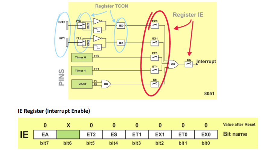
EA – global interrupt enable/disable:
o 0 – disables all interrupt requests.
o 1 – enables all individual interrupt requests.
ES – enables or disables serial interrupt:
o 0 – UART system cannot generate an interrupt.
o 1 – UART system enables an interrupt.
ET1 – bit enables or disables Timer 1 interrupt:
o 0 – Timer 1 cannot generate an interrupt.
o 1 – Timer 1 enables an interrupt.
EX1 – bit enables or disables external 1 interrupt:
o 0 – change of the pin INT0 logic state cannot generate an interrupt.
o 1 – enables an external interrupt on the pin INT0 state change.
ET0 – bit enables or disables timer 0 interrupt:
o 0 – Timer 0 cannot generate an interrupt.
o 1 – enables timer 0 interrupt.
EX0 – bit enables or disables external 0 interrupt:
o 0 – change of the INT1 pin logic state cannot generate an interrupt.
o 1 – enables an external interrupt on the pin INT1 state change.
If an interrupt of higher priority arrives while an interrupt is in progress, it will be immediately stopped and the higher priority interrupt will be executed first.
If two interrupt requests, at different priority levels, arrive at the same time then the higher priority interrupt is serviced first.
If both interrupt requests, at the same priority level, occur one after another, the one which came later has to wait until routine being in progress ends.
If two interrupt requests of equal priority arrive at the same time then the interrupt to be serviced is selected according to the following priority list:
1. External interrupt INT0
2. Timer 0 interrupt
3. External Interrupt INT1
4. Timer 1 interrupt
5. Serial Communication Interrupt IP Register (Interrupt Priority)
The IP register bits specify the priority level of each interrupt (high or low priority).

PS – Serial Port Interrupt priority bit
o Priority 0
o Priority 1
PT1 – Timer 1 interrupt priority
o Priority 0
o Priority 1
PX1 – External Interrupt INT1 priority
o Priority 0
o Priority 1
PT0 – Timer 0 Interrupt Priority
o Priority 0
o Priority 1
PX0 – External Interrupt INT0 Priority
o Priority 0
o Priority 1
When an interrupt request happens the following occurs:
1. Instruction in progress is ended.
2. The address of the next instruction to execute is pushed on the stack.
3. Depending on which interrupt is requested, one of 5 vectors (addresses) is written to the program counter in accordance to the table below:

These addresses store appropriate subroutines processing interrupts. Instead of them, there are usually jump instructions specifying locations on which these subroutines reside.
When an interrupt routine is executed, the address of the next instruction to execute is popped from the stack to the program counter and interrupted program resumes operation from where it left off.
A given Assembly language program is a series of statements, or lines. Assembly language instructions tell the CPU what to do.
Directives (or pseudo-instructions) Give directions to the assembler. Assembling and running an 8051 program
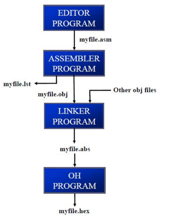
The step of Assembly language program are outlines as follows:
1) First, we use an editor to type a program for excellent editors or word processors are available that can be used to create and/or edit the program. Notice that the editor must be able to produce an ASCII file. For many assemblers, the file names follow the usual DOS conventions, but the source file has the extension “asm“ or “src”, depending on which assembly used.
2) The “asm” source file containing the program code created in step 1 is fed to an 8051assembler. The assembler converts the instructions into machine code. The assembler will produce an object file and a list file. The extension for the object file is “obj” while the extension for the list file is “lst”.
3) Assembler require a third step called linking. The linker program takes one or more object code files and produce an absolute object file with the extension “abs”. This abs file is used by 8051 trainers that have a monitor program.
4) Next the “abs” file is fed into a program called “OH” (object to hex converter) which creates a file with extension “hex” that is ready to burn into ROM.
4. 10 Operand Types
They are
Immediate Addressing Mode
MOV A, #6AH
In general we can write MOV A, #data
This addressing mode is named as “immediate” because it transfers an 8-bit data immediately to the accumulator (destination operand).
Example
MOV A, 04H
Here 04H is the address of register 4 of register bank#0. When this instruction is executed, what ever data is stored in register 04H is moved to accumulator. In the picture below we can see, register 04H holds the data 1FH. So the data 1FH is moved to accumulator.
Register Direct Addressing Mode
In this addressing mode we use the register name directly (as source operand). An example is shown below.
MOV A, R4
S,o we see that opcode for MOV A, R4 is EC. The opcode is stored in program memory address 0202 and when it is executed the control goes directly to R4 of the respected register bank that is selected in PSW.
Register Indirect Addressing Mode
So, in this addressing mode, address of the data (source data to transfer) is given in the register operand.
MOV A, @R0
Here the value inside R0 is considered as an address, which holds the data to be transferred to accumulator.
Example: If R0 holds the value 20H, and we have a data 2F H stored at the address 20H, then the value 2FH will get transferred to accumulator after executing this instruction.
Indexed Addressing Mode
MOVC A, @A+DPTR and MOVC A, @A+PC
Where DPTR is data pointer and PC is program counter (both are 16 bit registers).
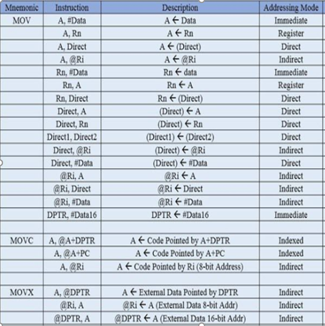
The Data Transfer Instructions relate to transfer of data between registers or external program memory or data memory. The Mnemonics associated with Data Transfer are given below.
- MOV
- MOVC
- MOVX
- PUSH
- POP
- XCH
- XCHD

Arithmetic Instructions
Using Arithmetic Instructions, one can perform addition, subtraction, multiplication and division. It consists of increment by one, decrement by one and a special instruction called Decimal Adjust Accumulator.
The Mnemonics associated with the Arithmetic Instructions of the 8051 Microcontroller Instruction Set are:
- ADD
- ADDC
- SUBB
- INC
- DEC
- MUL
- DIV
- DA A
The arithmetic instructions have no knowledge about the data format that is signed, unsigned, ASCII, BCD, and so on. The operations performed by the arithmetic instructions affect flags like carry, overflow, zero, etc. in PSW Register.
Mnemonic | Instruction | Description | Addressing Mode |
ADD | A,#data | A <- A + Data | Immediate |
| A,Rn | A<- A + Rn | Register |
| A,Direct | A<- A + (Direct) | Direct |
| A,@Ri | A<- A + @Ri | Indirect |
|
|
|
|
ADDC | A,#data | A <- A + Data + C | Immediate |
| A,Rn | A<- A + Rn + C | Register |
| A,Direct | A<- A + (Direct)+C | Direct |
| A,@Ri | A<- A + @Ri +C | Indirect |
|
|
|
|
SUBB | A,#data | A <- A – Data | Immediate |
| A,Rn | A<- A- Rn | Register |
| A,Direct | A<- A - (Direct) | Direct |
| A,@Ri | A<- A XRL-Ri | Indirect |
|
|
|
|
MUL AB | Multiply A with B |
|
|
|
|
|
|
DIV AB | Divide A by B |
|
|
|
|
|
|
DEC A | A,#data | A <- A -1 |
|
| A,Rn | Rn <-Rn -1 |
|
| A,Direct | (Direct) <- (Direct) -1 |
|
| A,@Ri | @Ri<- @Ri -1 |
|
INC A | A,#data | A <- A+1 |
|
| A,Rn | Rn <-Rn +1 |
|
| A,Direct | (Direct)<- (Direct) +1 |
|
| A,@Ri | @Ri<- @Ri+1 |
|
DA | A | Decimal Adjust Accumulator |
|
Logical Instructions
Logical Instructions perform logical operations like AND, OR, XOR, NOT, Rotate, Clear and Swap. Logical Instruction are performed on bytes of data on a bit-by-bit basis.
Mnemonics associated with Logical Instructions are as follows:
- ANL
- ORL
- XRL
- CLR
- CPL
- RL
- RLC
- RR
- RRC
- SWAP
Mnemonic | Instruction | Description | Addressing Mode |
ANL | A,#data | A <- A AND Data | Immediate |
| A,Rn | A<- A AND Rn | Register |
| A,Direct | A<- A AND (Direct) | Direct |
| A,@Ri | A<- A AND @Ri | Indirect |
| Direct A | (Direct ) <- (Direct ) AND A | Direct |
| Direct , # Data | (Direct ) <- (Direct ) AND # Data | Direct |
|
|
|
|
ORL | A,#data | A <- A OR Data | Immediate |
| A,Rn | A<- A OR Rn | Register |
| A,Direct | A<- A OR (Direct) | Direct |
| A,@Ri | A<- A OR @Ri | Indirect |
| Direct A | (Direct ) <- (Direct ) OR A | Direct |
| Direct , # Data | (Direct ) <- (Direct ) OR # Data | Direct |
|
|
|
|
XRL | A,#data | A <- A XRL Data | Immediate |
| A,Rn | A<- A XRL Rn | Register |
| A,Direct | A<- A XRL (Direct) | Direct |
| A,@Ri | A<- A XRL @Ri | Indirect |
| Direct A | (Direct ) <- (Direct ) XRL A | Direct |
| Direct , # Data | (Direct ) <- (Direct ) XRL # Data | Direct |
|
|
|
|
CLR | A | A<-00H |
|
CPL | A | A<-A |
|
|
|
|
|
RL | A | Rotate ACC Left |
|
|
|
|
|
RLC | A | Rotate ACC Left through carry |
|
RR | A | Rotate ACC right |
|
|
|
|
|
RRC | A | Rotate ACC right through carry |
|
SWAP | A | Swap nibbles within ACC |
|
8051 microcontroller has two Timers designated as Timer0 and Timer1. Each of these timers is assigned a 16-bit register.
The value of a Timer register increases by one every time a timer counts. Timer takes a time period of one machine cycle to count one. Machine cycle is defined as a unit that refers to the time required by the microcontroller to execute instructions. This means that the maximum number of times a timer can count without repeating is 216, i.e., 65536. So, the maximum allowed counts in value of Timer registers can be from 0000H to FFFFH.
Since 8051 is an 8 bit controller, the registers of 8051 Timers are accessed as two different registers; one for lower byte and other for higher byte.
For example, register of Timer0 is accessed as TL0 for lower byte and TH0 for higher byte. Similarly, TL1 and TH1 are registers assigned to Timer 1.
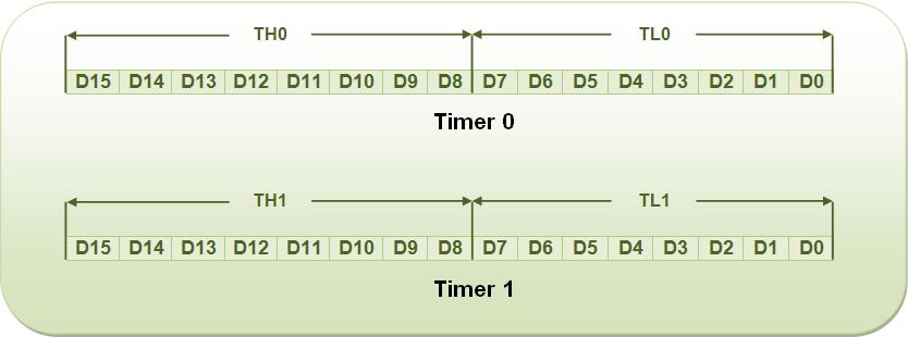
Bit Values of Timer 0 and Timer 1 of 8051 Microcontroller
8051 Timer Issues
While using 8051 Timers certain factors need to be considered, like whether the Timer is to be used for time keeping or for counting; whether the source for time generation is external clock or the controller itself; how many bits of Timer register are to be used or left unused.
How a Timer functions
The registers of Timers are loaded with some initial value. The value of a Timer register increases by one after every machine cycle. One machine cycle duration is the 1/12th of the frequency of the crystal attached to the controller.
For example, if the frequency of the crystal is 12 MHz, then the frequency for Timer will be 1MHz (1/12 of crystal frequency) and hence the time (T = 1/f) taken by the Timer to count by one is 1µs (1/1MHz). Similarly if an 11.0592 MHz crystal is used, operating frequency of Timer is 921.6 KHz and the time period is 1.085 µs.
If no value is loaded into the Timer, it starts counting from 0000H.
When the Timer reaches FFFFH, it reloads to 0000H. This roll over is communicated to the controller by raising a flag corresponding to that Timer, i.e., a flag bit is raised (set high) when the timer starts counting from 0000H again. TF0 and TF1 are the Timer flags corresponding to Timers 0 and 1.
These flags must be cleared (set low) by software every time they are raised. The Timer may terminate updating register values after a roll over or continue with its operation.

Image showing Status of Timer Flag on Roll Over
Starting or stopping a Timer
For every Timer, there is a corresponding Timer control bit which can be set or cleared by the program to start or stop the Timer. TR0 and TR1 are the control bits for Timers 0 and 1 respectively. Setting the control bit would start the Timer.
TR0 = 1; starts Timer 0
TR1 = 1; starts Timer 1
Clearing the control bit would stop the Timer.
TR0 = 0; stops Timer 0
TR1 = 0; stops Timer1
Configuring a Timer
A register called TMOD is used for configuring the Timers for the desired operation. TMOD is an 8-bit register with following bit configuration:

Bit Values of TMOD Register of 8051 Microcontroller
The lower four bits (TMOD.0 – TMOD.3) are used to configure Timer 0 while the higher four bits (TMOD.4 – TMOD.7) are for Timer 1. When GATE is high, the corresponding Timer is enabled only when there is an interrupt at corresponding INTx pin of AT89C51 controller and Timer control bit is high. Otherwise only setting Timer control bit is sufficient to start the Timer.
If C/T is low, Timer is used for time keeping, i.e., Timer updates its value automatically corresponding to 8051 clock source. When C/T is high, Timer is used as counter, i.e., it updates its value when it receives pulse from outside the 8051 controller.
M1 and M0 bits decide the Timer modes. There are four Timer modes designated as Modes 0, 1, 2 and 3.
Modes 1 and 2 are most commonly used while working with Timers.
TMOD = 0x01; sets the mode1 of Timer0 used for timing
TMOD = 0x20; sets the mode2 of Timer1 used for timing
Programming 8051 Timers
The programming of 8051 Timers can be done by using either polling method or by using interrupt. In polling, the microcontroller keeps monitoring the status of Timer flag. While doing so, it does no other operation and consumes all its processing time in checking the Timer flag until it is raised on a rollover. In interrupt method controller responds to only when the Timer flag is raised. The interrupt method prevents the wastage of controller’s processing time unlike polling method.
Polling is mostly used for time delay generation and interrupt method is more useful when waveforms are to be generated or some action has to be repeated in fixed delays.
(i) Polling Method
The polling method involves the following algorithm:
1. Configure the Timer mode by passing a hex value into the TMOD register. This will tell the controller about which Timer is be used; the mode of Timer; operation (to be used as timer or counter); and whether external interrupt is required to start Timer.
2. Load the initial values in the Timer low TLx and high THx byte. (x = 0/1)
3. Start the Timer by setting TRx bit.
4. Wait while the Timer flag TFx is raised.
5. Clear the Timer flag. The Timer flag is raised when Timer rolls over from FFFFH to 0000H. If the Timer is not stopped, it will start updating from 0000H in case of modes 0 & 1 while with initial value in case of mode 2. If TFx is not cleared, controller will not be able to detect next rollover.
6. Stop the Timer by clearing TRx bit. If TRx bit is not cleared the Timer will restart updating from 0000H after the rollover in case of modes 0 and 1 while with initial value in case of mode 2.
(ii) Interrupt Method
The interrupt method makes use of a register called Interrupt Enable (IE) register. An 8051 microcontroller has 6 hardware interrupts. The interrupts refer to a notification, communicated to the controller, by a hardware device or software, on receipt of which controller skips temporarily whatsoever it was doing and responds to the interrupt.
The controller starts the execution of an Interrupt Service Routine (ISR) or Interrupt Handler which is a piece of code that tells the processor or controller what to do on receipt of an interrupt. After the execution of ISR, controller returns to whatever it was doing earlier (before the interrupt was received).
The Interrupt Enable register has the following bits which enable or disable the hardware interrupts of 8051 microcontroller.

Bit Values of IE
When EA (IE.7) is set (=1), interrupts are enabled. When clear (EA=0), interrupts are disabled and controller does not respond to any interrupts.
ET0, ET1 & ET2 (IE.3, IE.4 & IE.5) are Timer interrupt bits. When set (high) the timer are enabled and when cleared (low) they are disabled. (8052 controllers have three Timers, so ET2 is its Timer 2 interrupt bit.) The ISR corresponding to these interrupts are executed when the TFx flags of respective Timers are raised. For more details on other IE register bits,
Timer programming using Timer interrupts involves following algorithm.
1. Configure the Timer mode by passing a hex value to TMOD register.
2. Load the initial values in the Timer low TLx and high THx byte.
3. Enable the Timer interrupt by passing hex value to IE register or setting required bits of IE register. For example,
IE = 0x82; enables Timer 0 interrupt
IE = 0x88; enables Timer 1 interrupt
Or
EA = 1;
ET0 = 1; enables Timer 0 interrupt
IE^7 = 1;
IE^3 = 1; enables Timer 1 interrupt
4. Start the Timer by setting TRx bit.
5. Write Interrupt Service Routine (ISR) for the Timer interrupt. For example,
ISR definition for Timer 0 :
Void ISR_Timer0(void) interrupt 1
{
<Body of ISR>
}
ISR definition for Timer 1 :
Void ISR_Timer1(void) interrupt 3
{
<Body of ISR>
}
6. If the Timer has to be stopped after once the interrupt has occurred, the ISR must contain the statement to stop the Timer.
For example,
Void ISR_Timer1(void) interrupt 3
{
<Body of ISR>
TR1 =0;
}
7. If a routine written for Timer interrupt has to be repeated again and again, the Timer run bit need not be cleared. But it should be kept in mind that Timer will start updating from 0000H and not the initial values in case of mode 0 and 1. So the initial values must be reloaded in the interrupt service routine.
For example,
Void ISR_Timer1(void) interrupt 3
{
<Body of ISR>
TH1 =0XFF; //load with initial values if in mode 0 or 1
TL1 = 0xFC;
}
Different modes of a Timer
There are four Timer modes designated as Modes 0, 1, 2 and 3. A particular mode is selected by configuring the M1 & M0 bits of TMOD register.
Mode | M1 | M0 | Operation |
Mode 0 | 0 | 0 | 13-bit Timer |
Mode 1 | 0 | 1 | 16-bit Timer |
Mode 2 | 1 | 0 | 8-bit Auto Reload |
Mode 3 | 1 | 1 | Split Timer Mode |
(i) Mode 0 : 13-bit Timer
Mode 0 is a 13 bit Timer mode and uses 8 bits of high byte and 5 bit prescaler of low byte. The value that the Timer can update in mode0 is from 0000H to 1FFFH. The 5 bits of lower byte append with the bits of higher byte. The Timer rolls over from 1FFFH to 0000H to raise the Timer flag.
(ii) Mode 1 : 16-bit Timer
Mode1 is one of the most commonly used Timer modes. It allows all 16 bits to be used for the Timer and so it allows values to vary from 0000H to FFFFH.
If a value, say YYXXH, is loaded into the Timer bytes, then the delay produced by the Timer will be equal to the product :
[ ( FFFFH – YYXXH +1 ) x ( period of one timer clock ) ].
It can also be considered as follows: convert YYXXH into decimal, say NNNNN, then delay will be equal to the product :
[ ( 65536-NNNNN ) x ( period of one timer clock ) ].
The period of one timer clock is 1.085 µs for a crystal of 11.0592 MHz frequency as discussed above.
In order to produce a desired delay, divide the required delay by the Timer clock period. Assume that the division yields a number NNNNN. This is the number of times Timer must be updated before it stops. Subtract this number from 65536 (binary equivalent of FFFFH) and convert the difference into hex. This will be the initial value to be loaded into the Timer to get the desired delay.
The calculator application in Windows can be a handy tool to carry out these calculations.
Example code
Time delay in Mode1 using polling method
// Use of Timer mode 1 for blinking LED using polling method
// XTAL frequency 11.0592MHz
#include<reg51.h>
Sbit led = P1^0; // LED connected to 1st pin of port P1
Void delay();
Main()
{
Unsigned int i;
While(1)
{
Led=~led; // Toggle LED
For(i=0;i<1000;i++)
Delay(); // Call delay
}
}
Void delay() // Delay generation using Timer 0 mode 1
{
TMOD = 0x01; // Mode1 of Timer0
TH0= 0xFC; // FC66 evaluated hex value for 1millisecond delay
TL0 = 0x66;
TR0 = 1; // Start Timer
While(TF0 == 0); // Using polling method
TR0 = 0; // Stop Timer
TF0 = 0; // Clear flag
}
Example code
Time delay in Mode1 using interrupt method
// Use of Timer mode 1 for blinking LED with interrupt method
// XTAL frequency 11.0592MHz
#include<reg51.h>
Sbit LED = P1^0; // LED connected to 1st pin of port P1
Void Timer(void) interrupt 1 // Interrupt No.1 for Timer 0
{
Led=~led; // Toggle LED on interrupt
}
Main()
{
TMOD = 0x01; // Mode1 of Timer0
TH0=0x00; // Initial values loaded to Timer
TL0=0x00;
IE = 0x82; // Enable interrupt
TR0=1; // Start Timer
While(1); // Do nothing
}
(iii) Mode 2 : 8-bit Auto Reload
Mode 2 is an 8 bit mode. The initial value is loaded into the higher byte. A copy of the same is passed to the lower byte. The Timer can update from 00H to FFH. The Timer rolls over from FFH to initial value automatically.
Mode 2 is commonly used for setting baud rates for serial communication.
Example code
Time delay in Mode2 using polling method
// Use of Timer mode 2 for blinking LED with polling method
// XTAL frequency 11.0592MHz
#include<reg51.h>
Sbit led = P1^0; // LED connected to 1st pin of port P1void delay();
Main()
{
Unsigned int i;
While(1)
{
Led=~led; // Toggle LED
For(i=0;i<1000;i++)
Delay(); // Call delay
}
}
Void delay()
{
TMOD = 0x02; // Mode1 of Timer0
TH0= 0xA2; // Initial value loaded to Timer
TR0 = 1; // Start Timer
While(TF0 == 0); // Polling for flag bit
TR0 = 0; // Stop Timer
TF0 = 0; // Clear flag
}
(iv) Mode 3 : Split Timer
In mode 3, also known as split mode, the Timer breaks into two 8-bit Timers that can count from 00H up to FFH. The initial values are loaded into the higher byte and lower byte of the Timer. In this case the start and flag bits associated with the other Timer are now associated with high byte Timer. So one cannot start or stop the other Timer. The other Timer can be used in modes 0, 1 or 2 and is updated automatically for every machine cycle.
For example, if Timer0 is used in split mode, TH0 and TL0 will become separate Timers. The start and flag bits associated with Timer1 will now be associated with the TH0. Timer 1 cannot be stopped or started, but will be updated for every machine cycle.
Split mode is useful when two Timers are required in addition to a baud rate generator.
Interrupt Structure of 8051 Microcontroller
After 'RESET' all the interrupts get disabled, and therefore, all the interrupts is enabled by software. From all the five interrupts, if anyone or all interrupt are activated, this will sets the corresponding interrupt flags as represent in the figure which corresponds to Interrupt structure of 8051 microcontroller:-
Interrupts in 8051 Microcontroller
All the interrupts can be set or cleared by some special function register that is also known as interrupt enabled (IE), and it is totally depends on the priority, which is executed by using interrupt priority register.
Interrupt Enable (IE) Register
IE register is used for enabling and disabling the interrupt. This is a bit addressable register in which EA value must be set to one for enabling interrupts. The individual bits in this register enables the particular interrupt like timer, serial and external inputs. Consider in the below IE register, bit corresponds to 1 activate the interrupt and 0 disable the interrupt.
Interrupt Priority Register (IP)
Using IP register it is possible to change the priority levels of an interrupts by clearing or setting the individual bit in the Interrupt priority (IP) register as shown in figure. It allows the low priority interrupt can interrupt the high-priority interrupt, but it prohibits the interruption by using another low-priority interrupt. If the priorities of interrupt are not programmed, then microcontroller executes the instruction in a predefined manner and its order are INT0, TF0, INT1, TF1, and SI.
Interrupt programming in 8051
Timer Interrupt Programming: In microcontroller Timer 1 and Timer 0 interrupts are generated by time register bits TF0 AND TF1. This timer interrupts programming by C code involves:
Selecting the configuration of TMOD register and their mode of operation.
Enables the IE registers and corresponding timer bits in it.
Choose and load the initial values of TLx and THx by using appropriate mode of operation.
Set the timer run bit for starting the timer.
Write the subroutine for a timer and clears the value of TRx at the end of the subroutine.
Let's see the timer interrupt programming using Timer0 model for blinking LED using interrupt method:
#include< reg51 .h>
Sbit Blink Led = P2^0; // LED is connected to port 2 Zeroth pin
Void timer0_ISR (void) interrupt 1 //interrupt no. 1 for Timer0
{
Blink Led=~Blink Led; // Blink LED on interrupt
TH0=0xFC; // loading initial values to timer
TL0=0x66;
}
Void main()
{
TMOD=0x0l; // mode 1 of Timer0
TH0 = 0xFC: // initial value is loaded to timer
TL0 = 0x66:
ET0 =1; // enable timer 0 interrupt
TR0 = 1; // start timer
While (1); // do nothing
}
External Hardware Interrupt Programming
Microcontroller 8051 is consisting of two external hardware interrupts: INT0 and INT1 as discussed above. These interrupts are enabled at pin 3.2 and pin 3.3. It can be level triggered or edge triggered. In level triggering, low signal at pin 3.2 enables the interrupt, while at pin 3.2 high to low transition enables the edge triggered interrupt.
Enables the equivalent bit of external interrupt in Interrupt Enable (IE) register.
If it is level triggering, then write subroutine appropriate to this interrupt, or else enable the bit in TCON register corresponding to the edge triggered interrupt.
Consider the edge triggered external hardware interrupt programming is:-
Void main()
{
IT0 = 1; // Configure interrupt 0 for falling edge on INT0
EXO = 1; // Enabling the EX0 interrupt
EA =1; // Enabling the global interrupt flag
}
Void ISR_ex0(void) interrupt 0
{
<body of interrupt>
}
Serial Communication Interrupt Programming
It is used when there is a need to send or receive data. Since one interrupt bit is used for both Transfer Interrupt (TI) and Receiver Interrupt (RI) flags, Interrupt Service Routine (ISR) must examine these flags for knowing the actual interrupt. By the logical OR operation of RI and TI flags causes the interrupt and it is clear by the software alone. Consider the steps involved in serial communication interrupt programming are:-
Configure the Interrupt Enable register for enabling serial interrupt.
Configure the SCON register for performing transferring and receiving operation.
Write a subroutine for given interrupt with appropriate function.
Program for sending 'E' through serial port with 9600 baud rate using Serial Interrupt:
Void main()
{
TMOD = 0x20:
TH1= 0xFD; // baud rate for 9600 bps
SCON = 0x50;
TR1=1;
EA=l;
Whlle(l);
}
Void ISR_Serial(void) interrupt 4
{
If(TI==l)
{
SBUF= ?E?;
TI=0;
}
Else
RI =0;
}
References:
- The 8051 Microcontroller and Embedded Systems using Assembly and C -by Muhammad Ali Mazidi.
8051 Microcontrollers: an Applications Based Introduction Book by David Calcutt, Frederick Cowan, and G. Hassan Parchizadeh
8051 Microcontroller Book by Kenneth Ayala