Unit-1
Introduction
The elements which form a digital communication system is represented by the following block diagram for the ease of understanding.
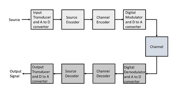
Fig 1 Elements of Digital Communication System
Following are the sections of the digital communication system.
Source
The source can be an analog signal.
Example: A Sound signal
Input Transducer
This is a transducer which takes a physical input and converts it to an electrical signal. This block also consists of an analog to digital converter where a digital signal is needed for further processes.
A digital signal is generally represented by a binary sequence.
Source Encoder
The source encoder compresses the data into minimum number of bits. This process helps in effective utilization of the bandwidth. It removes the redundant bits unnecessary excess bits, i.e. ,zeroes.
Channel Encoder
The channel encoder, does the coding for error correction. During the transmission of the signal, due to the noise in the channel, the signal may get altered and hence to avoid this, the channel encoder adds some redundant bits to the transmitted data. These are the error correcting bits.
Digital Modulator
The signal to be transmitted is modulated here by a carrier. The signal is also converted to analog from the digital sequence, in order to make it travel through the channel or medium.
Channel
The channel or a medium, allows the analog signal to transmit from the transmitter end to the receiver end.
Digital Demodulator
This is the first step at the receiver end. The received signal is demodulated as well as converted again from analog to digital. The signal gets reconstructed here.
Channel Decoder
The channel decoder, after detecting the sequence, does some error corrections. The distortions which might occur during the transmission, are corrected by adding some redundant bits. This addition of bits helps in the complete recovery of the original signal.
Source Decoder
The resultant signal is once again digitized by sampling and quantizing so that the pure digital output is obtained without the loss of information. The source decoder recreates the source output.
Output Transducer
This is the last block which converts the signal into the original physical form, which was at the input of the transmitter. It converts the electrical signal into physical output.
Output Signal
This is the output which is produced after the whole process.
Key takeaway
The channel decoder, after detecting the sequence, does some error corrections. The distortions which might occur during the transmission, are corrected by adding some redundant bits.
PARAMETERS | ANALOG COMMUNICATION | DIGITAL COMMUNICATION |
Definition | Analog Communication is the technology which uses Analog signal for the transmission of information. | Digital Communication is the technology which uses digital signal for the transmission of information. |
Noise and Distortion | Get affected by Noise | Immune from Noise and Distortion |
Error Probability | Error Probability is high due to parallax. | Error Probability is low |
Hardware | Hardware is complicated and less flexible than digital system. | Hardware is flexible and less complicated than Analog system. |
Cost | Low Cost | High Cost |
Bandwidth Requirement | Low bandwidth requirement | High bandwidth Requirement |
Power Requirement | High power is required | Low Power Requirement |
Portability | Less Portable as the components are heavy | More portable due to compact equipments. |
Modulation Used | Amplitude and Angle Modulation | Pulse coded Modulation or PCM, DPCM etc. |
Representation of Signal | Analog signal can be represented by sine wave. | Digital signal is represented by square wave. |
Signal Values | Consists of continuous values | Consists of discrete values |
Example of Signal | Analog signal comprises of voice, sound etc. | Digital signals are used in computers |
Sampling is defined as, “The process of measuring the instantaneous values of continuous-time signal in a discrete form.”
Sample is a piece of data taken from the whole data which is continuous in the time domain.
When a source generates an analog signal and if that has to be digitized, having 1s and 0s i.e., High or Low, the signal has to be discretized in time. This discretization of analog signal is called as Sampling.
The following figure indicates a continuous-time signal x (t) and a sampled signal xs (t). When x (t) is multiplied by a periodic impulse train, the sampled signal xs (t) is obtained.
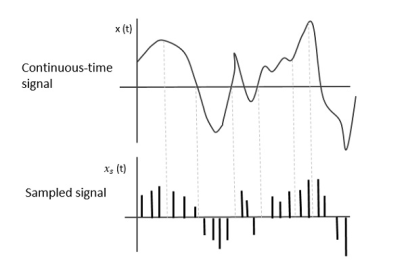
Fig 2 Sampled Signal
Sampling Rate
To discretize the signals, the gap between the samples should be fixed. That gap can be termed as a sampling period Ts.
Sampling Frequency=1/Ts=fs
Where,
Sampling frequency is the reciprocal of the sampling period. This sampling frequency, can be simply called as Sampling rate. The sampling rate denotes the number of samples taken per second, or for a finite set of values.
Nyquist Rate
Suppose that a signal is band-limited with no frequency components higher than W Hertz. That means, W is the highest frequency. For such a signal, for effective reproduction of the original signal, the sampling rate should be twice the highest frequency.
Which means,
fS=2W
Where,
This rate of sampling is called as Nyquist rate.
Sampling Theorem
The sampling theorem, which is also called as Nyquist theorem, delivers the theory of sufficient sample rate in terms of bandwidth for the class of functions that are bandlimited.
The sampling theorem states that, “a signal can be exactly reproduced if it is sampled at the rate fs which is greater than twice the maximum frequency W.”
Let us consider a band-limited signal, i.e., a signal whose value is non-zero between some –W and W Hertz.
Such a signal is represented as x(f)=0 for ∣f∣>W
For the continuous-time signal x (t), the band-limited signal in frequency domain, can be represented as shown in the following figure.
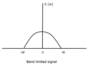
Fig 3 Band limited Signal
If the signal x(t) is sampled above the Nyquist rate, the original signal can be recovered, and if it is sampled below the Nyquist rate, the signal cannot be recovered.
The following figure explains a signal, if sampled at a higher rate than 2w in the frequency domain.

Fig 4 Fourier Transform of xs(t)
The above figure shows the Fourier transform of a signal xs (t).
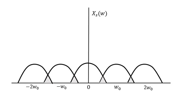
If fs<2W
The resultant pattern will look like the following figure.
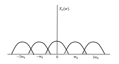
Fig 5 Output Waveform
Here, the over-lapping of information is done, which leads to mixing up and loss of information. This unwanted phenomenon of over-lapping is called as Aliasing.
Aliasing
Aliasing can be referred to as “the phenomenon of a high-frequency component in the spectrum of a signal, taking on the identity of a low-frequency component in the spectrum of its sampled version.”
Key Takeaways:
Examples:
The continuous-time signal x(t) = cos(200πt) is used as the input for a CD converter with the sampling period 1/300 sec. Determine the resultant discrete-time signal x[n].
Solution:
We know,
X[n] =x(nT)
= cos(200πnT)
= cos(2πn/3) , where n= -1,0,1,2……
The frequency in x(t) is 200π rad/s while that of x[n] is 2π/3.
Determine the Nyquist frequency and Nyquist rate for the continuous-time signal x(t) which has the form of:
X(t) = 1+ sin(2000πt) + cos (4000πt)
Solution:
The frequencies are 0, 2000π and 4000π.
The Nyquist frequency is 4000π rad/s and the Nyquist rate is 8000π rad/s.
Consider an analog signal 
Find the Nyquist rate?
Solution.
The frequency in the analog signal

The largest frequency is

The Nyquist rate is

The analog signal 


Solution.


For  ,the folding frequency is
Hence  is not effected by aliasing
 Is changed by the aliasing effect
 Is changed by the aliasing effect
So that normalizing frequencies are

The analog signal that we can recover is

Which is different than the original signal 
For 


Solution. a. 
The minimum sampling rate is

And the discrete time signal is

b. if  , the discrete time signal is

c. If Fs=75Hz , the discrete time signal is

d. For the sampling rate 
 in part in (c). Hence

So, the analog sinusoidal signal is


Suppose a continuous-time signal x(t) = cos (Ø0t) is sampled at a sampling frequency of 1000Hz to produce x[n]: x[n] = cos(πn/4)
Determine 2 possible positive values of Ø0, say, Ø1 and Ø2. Discuss if cos(Ø1t) or cos(Ø2t) will be obtained when passing through the DC converter.
Solution:
Taking T= 1/1000s
cos(πn/4) =x[n] = x(nT) = cos (Ø0n/1000)
Ø1 is easily computed as 
Ø1 = 250π
Ø2 can be obtained by noting the periodicity of a sinusoid:
 Ø2n/1000)
Ø2 = 2250π
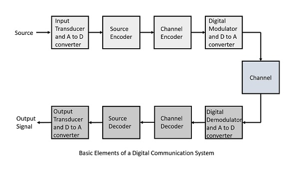
Fig 6 (a) Sampler (b) Output
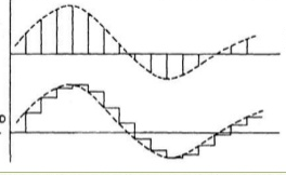
The sampled data signal is modified by the controller. The hold circuit than converts the signal to analog form. The simplest hold circuit is ZOH (zero order hold) in which the reconstructed signal acquires the same value as the last received sample for the entire sampling period.
The basic sampler is shown in above figure (a) and output in figure (b). The high frequency signal present in the reconstructed signal is filtered by the controller elements which are the low pass in frequency behaviour.
The first or higher order holds have no advantage over the ZOH. In the first order hold the last two signal samples are used to reconstruct the signal for the current sampling period.
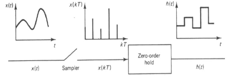
Data hold is a process of generating a continuous-time signal h(t) from a discrete time signal x(kT). The signal x(kT) can be approximated by a polynomial  as
as
h(kT+ )=an
)=an n+an-1
 n-1+….+a1
 +a0 0≤
 ≤ T
≤ T
h(kT)=x(kT)
h(kT+ )=an
)=an n+an-1
 n-1+….+a1
 +x(kT)
If the data hold circuit is an nth order polynomial it is called as nth order hold circuit.
Zero Order Hold (ZOH)
If n=0 in above equation the zero-order hold is obtained.
h(kT+ )= x(kT) 0≤
 ≤ T k=0,1,2,3…….
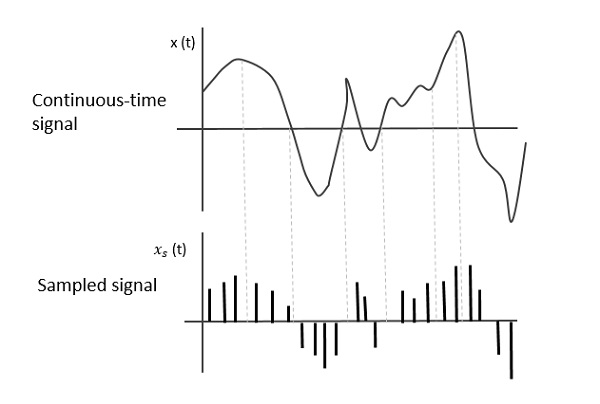
Fig 7 Zero Order Hold
h(t)=x(0)[u(t)-u(t-T)]+x(t)[u(t-T)-u(t-2T)]+x(2T)[u(t-2T)-u(t-3T)]……..
=
Taking Laplace transform of above equation we get
L[u(t-kT)] = 
L[h(t)]=L{ }
}
H(s)= =
= 
Gho(s)=
X*(s)=
The transfer function of ZOH is Gho(s)=
Key takeaway
The transfer function of ZOH is Gho(s)=
During transmission, noise is introduced at top of the transmission pulse which can be easily removed if the pulse is in the form of flat top. Here, the top of the samples are flat i.e. they have constant amplitude. Hence, it is called as flat top sampling or practical sampling. Flat top sampling makes use of sample and hold circuit.
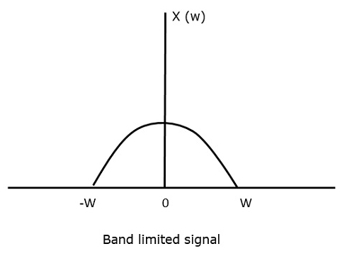
Fig 8 Flat top Sampled Signal
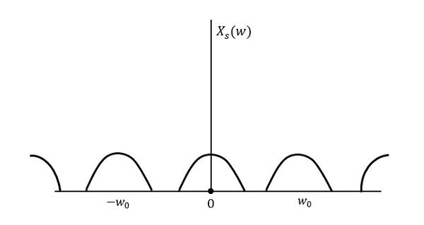
Fig 9 Flat top signal obtained after convolution
The sampled signal can be obtained by convolution of rectangular pulse p(t) with ideally sampled signal say yδ(t) as shown in the diagram above
y(t) = p(t) x yδ(t)
Taking F.T of above signal we get
From convolution
Key takeaway
The bandpass signal x(t) which maximum bandwidth is 2W can be completely represented into and recovered from its samples if it is sampled at the minimum rate of twice the bandwidth. The spectrum is centred around frequency fc. The bandwidth is 2W. Thus, the frequencies in the bandpass signals are from fc-W to fc+W. The bandpass signal is represented in its in-phase and quadrature components.

Fig 10 Spectrum of Bandpass Signal
x1(t) = in-phase component
xQ(t) = Quadrature component
Then signal x(t) can be written as
x(t) = x1(t)cos(2πfct)-xQ(t) sin (2 πfct)
The spectrum of the above signal is in between -W to +W. This is shown in below figure

Fig 11 Spectrum of in-phase and quadrature components of Bandpass signal x(t)
The reconstructed signal is then given by
X(t)=  πfc(t-
 )]
)]
From above equation we can conclude that
 = x(nTs)
Ts = 
Key takeaway
For bandpass signal with bandwidth 2W the minimum sampling rate is twice the bandwidth.
Quantization noise is a model of quantization error introduced by quantization in the analog-to-digital conversion (ADC). It is a rounding error between the analog input voltage to the ADC and the output digitized value. The noise is non-linear and signal-dependent.
There are two types of Quantization - Uniform Quantization and Non-uniform Quantization.
The type of quantization in which the quantization levels are uniformly spaced is termed as a Uniform Quantization.

Fig 12 Uniform Quantization
The type of quantization in which the quantization levels are unequal and mostly the relation between them is logarithmic, is termed as a Non-uniform Quantization.

Fig 13 Non-Uniform Quantization
Key takeaway
The type of quantization in which the quantization levels are uniformly spaced is termed as a Uniform Quantization. The type of quantization in which the quantization levels are unequal and mostly the relation between them is logarithmic, is termed as a Non-uniform Quantization.
The signal-to-noise ratio is
SNR = average signal power /average noise power
For uniform quantization noise
average signal power ≈ am2p (a ≈ 1 2 )
quantization error ≈ 1/3 (mp/L)2
SNR ≈ cL2 = c22m where m is the number of bits in the PCM sample, so L = 2m. c is a constant
SNR grows exponentially with the number of bits.
If we measure SNR in dB,
SNRdB = 10 log10(c22m) = 10 log10(c) + 2m log102 = (α + 6m)dB
where α = 10 log10 c.
Key takeaway
Increasing n by one bit improves SNR by 6 dB! One bit quadruples SNR.
References
1. “Communication Systems”, Simon Haykin, Wiley publication, 4th Edition, 2004
2. “Digital Communication Fundamentals and Applications”, Bernard Sklar, Pearson
Education India, 2nd Edition, 2009
3. “Modern Electronic Communication”, Miller Gary M, Prentice-Hall, 6th Edition, 1999
4. “Digital Communications”, John Proakis, Tata Mc Graw Hill, 5th Edition, 2007
5. “Electronic Communication Systems, Fundamentals Through Advanced”, Wayne Tomsi, Pearson Education, 4th Edition, 2001