Unit-5
Error
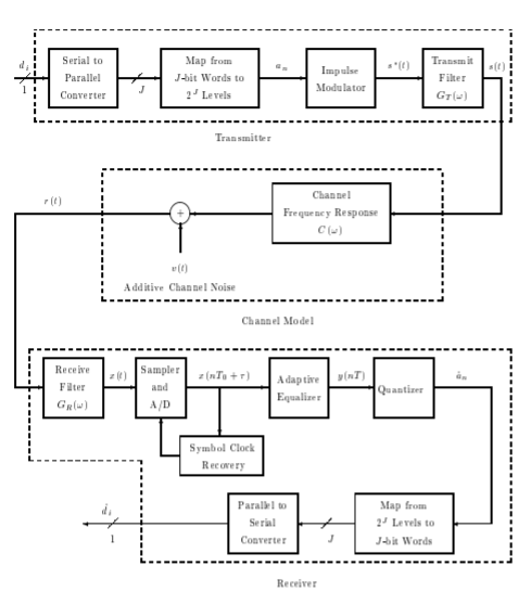
Fig 1 Baseband PAM Block Diagram
The transmitter input di is a serial binary data sequence with a bit rate of Rd bits/sec. Input bits are blocked into J-bit words by the serial-to-parallel converter. Input blocks are mapped into the sequence of symbols an which are selected from an alphabet of M = 2J distinct voltage levels. For example, the following levels uniformly spaced by 2d are commonly used:

The minimum level is −(M − 1)d and the maximum level is (M − 1)d. The symbol rate is fs = 1/T = Rd/J symbols/sec
The impulse modulator output is

The band limiting transmit filter output is

The channel is modelled as a filter C(ω) followed by an additive noise source. The receive filter eliminates out-of-band noise and, in conjunction with the transmit filter, forms a properly shaped pulse. The output of the receive filter is sampled at a rate that is an integer multiple N of the symbol rate fs. Typically, N might be 3 or 4. These samples are used by the Symbol Clock Recovery system to lock the receiver symbol clock to the transmitter clock.
The Adaptive Equalizer is an FIR filter with adjustable taps that automatically compensates for channel amplitude and phase distortion. It also corrects for small deviations in the transmit and receive filter responses from their ideal nominal values. A least mean-square error (LMS) adaptation algorithm is used most often. The equalizer output is sampled at the symbol rate and quantized to the nearest ideal level. The Quantizer output is mapped to the corresponding J-bit binary word and converted back to a serial output data sequence.
Key takeaway
The Adaptive Equalizer is an FIR filter with adjustable taps that automatically compensates for channel amplitude and phase distortion. It also corrects for small deviations in the transmit and receive filter responses from their ideal nominal values.
The analysis for  assumes perfectly white noise j (t) for simplicity. Note that a white noise j(t) has infinite power such that j (t) and c(t)j(t) will have the same PSD


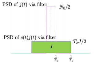
Fig 2 PDF Comparison
 )
)
An optimum filter is such a filter used for acquiring a best estimate of desired signal from noisy measurement. It is different from the classic filters. These filters are optimum because they are designed based on optimization theory to minimize the mean square error between a processed signal and a desired signal, or equivalently provides the best estimation of a desired signal from a measured noisy signal.
It is pervasive that when we measure a (desired) signal d(n), noise v(n) interferes with the signal so that a measured signal becomes a noisy signal
x(n) x(n)=d(n)+v(n)
It is also very common that a signal d(n) is distorted in its measurement (e.g., an electromagnetic signal distorts as it propagates over a radio channel). Assuming that the system causing distortion is characterized by an impulse response of h (n) s , the measurement of d(n) can be expressed by the sum of distorted signal s(n) and noise
v(n) x(n)=s(n)+v(n)= h (n)∗ s d(n)+v(n)
where s(n)= h (n)∗ s d(n).
If both d(n) and v(n) are assumed to be wide-sense stationary (WSS) random processes, then x(n) is also a WSS process. The signals that we discuss in this chapter will be WSS if they are not specially specified. If signal d(n) and measurement noise v(n) are assumed to be uncorrelated (this is true in many practical cases), then r (k) = r (k) = 0.
In this case, the noisy signal,
x(n)= h (n)∗ s d(n)+v(n),
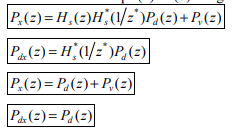
the relation of r (k) x with r (k ) d and r (k) v (the autocorrelations of x(n), d(n) and v(n), respectively) as follows,


For the noisy signal of the form x(n)= d(n)+v(n), a special case of where h (n) s =δ (n) and no distortion happens to d(n) in its measurement, we have


Optimum filtering is to acquire the best linear estimate of a desired signal from a measurement. The main issues in optimal filtering contain
• filtering that deals with recovering a desired signal d(n) from a noisy signal (or measurement) x(n);
• prediction that is concerned with predicting a signal d(n+m) for m>0 from observation x(n);
• smoothing that is an a posteriori form of estimation, i.e., estimating d(n+m) for m

Fig 3 Optimum Filtering
Matched Filter:
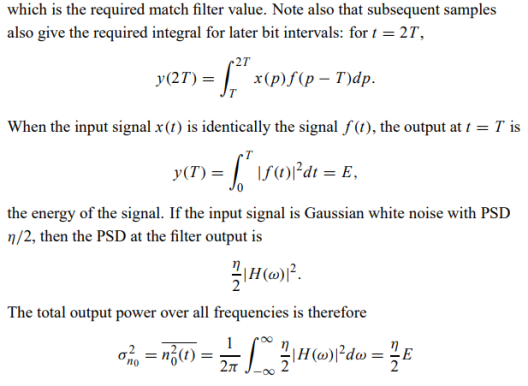
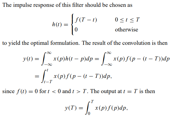
If a filter produces an output in such a way that it maximizes the ratio of output peak power to mean noise power in its frequency response, then that filter is called Matched filter.

Fig 4 Matched Filter
Frequency Response Function of Matched Filter
The frequency response of the Matched filter will be proportional to the complex conjugate of the input signal’s spectrum. Mathematically, we can write the expression for frequency response function, H(f) of the Matched filter as −
H(f)=GaS∗(f)e−j2πft1 ………..1
Where,
Ga is the maximum gain of the Matched filter
S(f) is the Fourier transform of the input signal, s(t)
S∗(f) is the complex conjugate of S(f)
t1 is the time instant at which the signal observed to be maximum
In general, the value of Ga is considered as one. We will get the following equation by substituting Ga=1in Equation 1.
H(f)=S∗(f)e−j2πft1 ……..2
The frequency response function, H(f) of the Matched filter is having the magnitude of S∗(f)and phase angle of e−j2πft1, which varies uniformly with frequency.
Impulse Response of Matched Filter
In time domain, we will get the output, h(t) of Matched filter receiver by applying the inverse Fourier transform of the frequency response function, H(f).
h(t)= ….….3
….….3
Substitute, Equation 1 in Equation 3.
h(t)=
⇒h(t)= ………4
………4
We know the following relation.
S∗(f)=S(−f) ……..5
Substitute, Equation 5 in Equation 4.
h(t)=
⇒h(t)=
⇒h(t)=Gas(t1−t)
In general, the value of Ga is considered as one. We will get the following equation by substituting Ga=1.
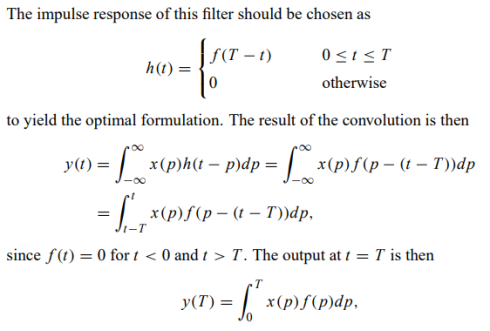
h(t)=s(t1−t)
The above equation proves that the impulse response of Matched filter is the mirror image of the received signal about a time instant t1. The following figures illustrate this concept.
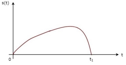
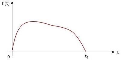
Fig 5 Impulse Response of Matched Filter
The received signal, s(t) and the impulse response, h(t) of the matched filter corresponding to the signal, s(t) are shown in the above figures.
Key takeaway
An optimum filter is such a filter used for acquiring a best estimate of desired signal from noisy measurement. It is different from the classic filters.
If a filter produces an output in such a way that it maximizes the ratio of output peak power to mean noise power in its frequency response, then that filter is called Matched filter.

5.5 Coherent reception
Coherent detection is well known in wireless communication systems. In those wireless systems, a radio frequency (RF) local oscillator (LO) is tuned to “heterodyne”, which is a signal processing technique which combine a high-frequency signal f1 with another f2 to produce a lower frequency signal (f1 – f2), with a received signal through an RF mixer, as shown in Fig.(a), so that both the amplitude and phase information contained in an RF carrier can be recovered in the following digital signal processor (DSP).
For an optical coherent system, a narrow-linewidth tunable laser, serving as an LO, tunes its frequency to “intradyne” with a received signal frequency through an optical coherent mixer, as shown in Fig. (b), and thereby recovers both the amplitude and phase information contained in a particular optical carrier.
Here, “intradyne” means that the frequency difference between an LO and a received optical carrier is small and within the bandwidth of the receiver, but does not have to be zero.
This implies that the frequency and phase of an LO do not have to be actively controlled to an extreme accuracy, therefore avoiding the use of a complicated optical phase locked loop.
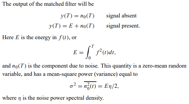
Fig 6 (a) RF Mixer (b) Optical Coherent mixer
In contrast to coherent detection is direct detection, typically used by 10Gb/s or lower-speed systems. In a direct detection receiver, its photo-detector only responds to changes in the receiving signal optical power, and cannot extract any phase or frequency information from the optical carrier.
Advantages of Coherent detection:
(1) Greatly improved receiver sensitivity.
(2) Can extract amplitude, frequency, and phase information from an optical carrier, and consequently can achieve much higher capacity in the same bandwidth.
(3) Its DSP can compensate very large chromatic and polarization mode dispersion due to optical fibers, and eliminate the need for optical dispersion compensators and the associated optical amplifiers.
(4) When using balanced detectors with a high common mode noise rejection ratio (CMRR), not only signal-to-noise ratio (SNR) can be improved further, but also agile wavelength selection can be achieved by LO tuning without the use of an optical filter or demultiplexer.
The laser phase noise of an LO is an important impairment in coherent systems as it impacts the “phase coherence”. The “linewidth” parameter of a laser diode is directly related to its phase noise.
Its impact has become as huge as what commercial laser diodes and erbium-doped fiber amplifiers have brought to the industry. Consequently, long-haul networks have already become coherent-centric today, while metro optical networks are bound to become coherent-centric in the next few years.
Key takeaway
Coherent detection is well known in wireless communication systems. In those wireless systems, a radio frequency (RF) local oscillator (LO) is tuned to “heterodyne”, which is a signal processing technique which combine a high-frequency signal f1 with another f2 to produce a lower frequency signal (f1 – f2)
FSK Modulator
The FSK modulator block diagram comprises of two oscillators with a clock and the input binary sequence. Following is its block diagram.

Fig.7: FSK modulator
The two oscillators, producing a higher and a lower frequency signals, are connected to a switch along with an internal clock. To avoid the abrupt phase discontinuities of the output waveform during the transmission of the message, a clock is applied to both the oscillators, internally. The binary input sequence is applied to the transmitter so as to choose the frequencies according to the binary input.
FSK Demodulator
There are different methods for demodulating a FSK wave. The main methods of FSK detection are asynchronous detector and synchronous detector. The synchronous detector is a coherent one, while asynchronous detector is a non-coherent one.
Asynchronous FSK Detector
The block diagram of Asynchronous FSK detector consists of two band pass filters, two envelope detectors, and a decision circuit. Following is the diagrammatic representation.
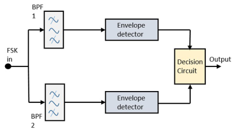
Fig.8: FSK demodulator
The FSK signal is passed through the two Band Pass Filters BPFs, tuned to Space and Mark frequencies. The output from these two BPFs look like ASK signal, which is given to the envelope detector. The signal in each envelope detector is modulated asynchronously.
The decision circuit chooses which output is more likely and selects it from any one of the envelope detectors. It also re-shapes the waveform to a rectangular one.
GENERATION AND COHERENT DETECTION OF BPSK SIGNALS
(i) Generation
To generate the BPSK signal, we build on the fact that the BPSK signal is a special case of DSB-SC modulation. Specifically, we use a product modulator consisting of two components.
(i) Non-return-to-zero level encoder, whereby the input binary data sequence is encoded in polar form with symbols 1 and 0 represented by the constant-amplitude.
(ii) Product modulator, which multiplies the level encoded binary wave by the sinusoidal carrier of amplitude to produce the BPSK signal. The timing pulses used to generate the level encoded binary wave and the sinusoidal carrier wave are usually, but not necessarily, extracted from a common master clock.
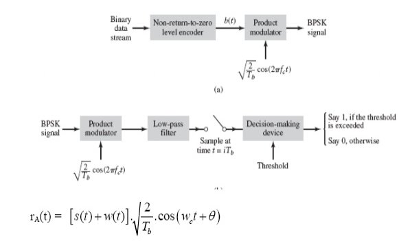
Fig. 9: Product modulator
(ii) Detection
To detect the original binary sequence of 1s and 0s, the BPSK signal at the channel output is applied to a receiver that consists of four sections
(a)Product modulator, which is also supplied with a locally generated reference signal that is a replica of the carrier wave
(b)Low-pass filter, designed to remove the double-frequency components of the product modulator output (i.e., the components centered on) and pass the zero-frequency components.
(c)Sampler, which uniformly samples the output of the low-pass filter at where; the local clock governing the operation of the sampler is synchronized with the clock responsible for bit-timing in the transmitter.
(d)Decision-making device, which compares the sampled value of the low-pass filters output to an externally supplied threshold, every seconds. If the threshold is exceeded, the device decides in favour of symbol 1; otherwise, it decides in favour of symbol 0. levels.
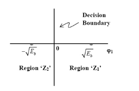
Fig. 10: Decision-making device


Fig.11: Decision-making device
GENERATION AND COHERENT DETECTION OF BFSK SIGNALS
(i) Generation
On-off level encoder:
Here, the output is of constant amplitude √Eb for input 1 and 0 for input 0.
Pair of oscillators:
Frequency f1 and f2 differ by integer multiple of 1/Tb. The lower oscillator has frequency f2 preceded by inverter. When in a signal interval, the input symbol is 1, the upper oscillator is switched on, and signal s1(t) is transmitted, while lower oscillator is switched off.
When input is 0, upper oscillator is off, lower oscillator is on and signal s2(t) is transmitted.
Fig.12: BFSK generation
(ii) Detection
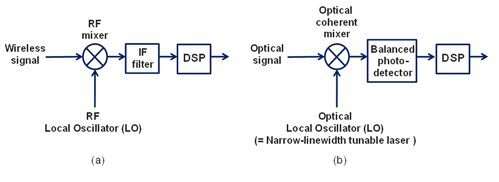
Fig.13: BFSK detection
It consists of two correlators with a common input, and reference signals Ø1(t), Ø2(t) are applied.
Then y = x1 – x2
The output y is compared with the threshold =0
If y>0 then output = 1 else 0.
But if y=0 then the receiver makes a random guess of 0 or 1.
Binary ASK
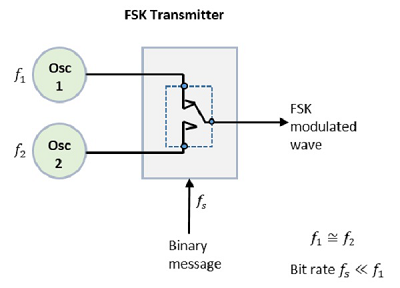
Fig 14 BASK Transmitter
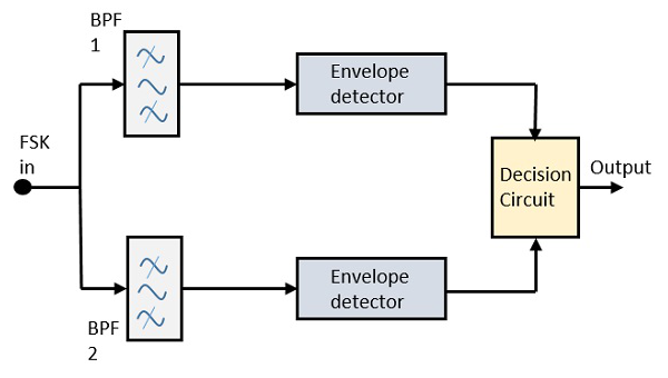
Fig 15 Coherent BASK Demodulation
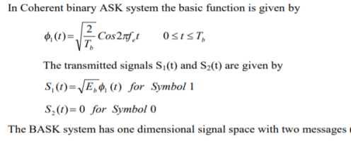
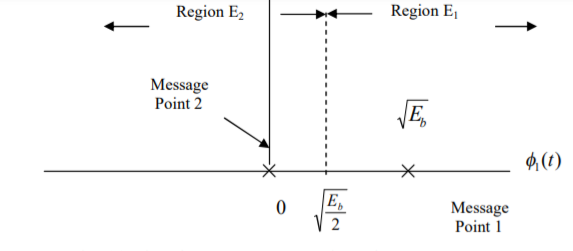
Fig 16 Signal Space Representation of BASK Signal
In transmitter the binary data sequence is given to an on-off encoder. Which gives an output  volts for symbol 1 and 0 volt for symbol 0. The resulting binary wave [in unipolar form] and sinusoidal carrier 1(t) is applied to a product modulator. The desired BASK wave is obtained at the modulator output. In demodulator, the received noisy BASK signal x(t) is apply to correlator with coherent reference signal 1(t) as shown in fig. (b). The correlator output x is compared with threshold λ.
If x > λ the receiver decides in favour of symbol 1.
If x < λ the receiver decides in favour of symbol 0.
Key Takeaways:
The FSK modulator block diagram comprises of two oscillators with a clock and the input binary sequence
The main methods of FSK detection are asynchronous detector and synchronous detector.
Non-Coherent Detection of ASK
Incoherent detection as used in analog communication does not require carrier for reconstruction. The simplest form of incoherent detector is the envelope detector as shown in figure below. The output of envelope detector is the baseband signal. Once the baseband signal is recovered, its samples are taken at regular intervals and compared with threshold. If Z(t) is greater than threshold ( ) a decision will be made in favour of symbol ‘1’ If Z(t) the sampled value is less than threshold ( ) a decision will be made in favour of symbol ‘0’

Fig 17 Envelop detection for BASK
Non-Coherent Detection of FSK

Fig 18 Non—Coherent Detection of FSK
Figure above shows the block diagram of incoherent type FSK demodulator. The detector consists of two band pass filters one tuned to each of the two frequencies used to communicate ‘0’s and ‘1’s., The output of filter is envelope detected and then baseband detected using an integrate and dump operation. The detector is simply evaluating which of two possible sinusoids is stronger at the receiver. If we take the difference of the outputs of the two envelope detectors the result is bipolar baseband. The resulting envelope detector outputs are sampled at t = kTb and their values are compared with the threshold and a decision will be made in favour of symbol 1 or 0.
The non-coherent detection of PSK is not possible.
QPSK
(i) Generation
The QPSK Modulator uses a bit-splitter, two multipliers with local oscillator, a 2-bit serial to parallel converter, and a summer circuit.
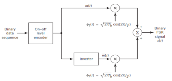
Fig.19: QPSK generation
At the modulator’s input, the message signal’s even bits (i.e., 2nd bit, 4th bit, 6th bit, etc.) and odd bits (i.e., 1st bit, 3rd bit, 5th bit, etc.) are separated by the bits splitter and are multiplied with the same carrier to generate odd BPSK (called as PSKI) and even BPSK (called as PSKQ). The PSKQ signal is anyhow phase shifted by 90° before being modulated.
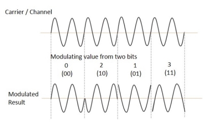
The QPSK waveform for two-bits input is as follows, which shows the modulated result for different instances of binary inputs.
(ii) Detection
The QPSK Demodulator uses two product demodulator circuits with local oscillator, two band pass filters, two integrator circuits, and a 2-bit parallel to serial converter.
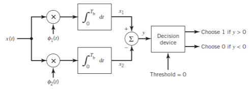
Fig.20: QPSK detectors
The two product detectors at the input of demodulator simultaneously demodulate the two BPSK signals. The pair of bits are recovered here from the original data. These signals after processing are passed to the parallel to serial converter.

Fig.21: QPSK output
Key takeaway

BFSK:


Based on the decision rule 


 is the variance of
Power spectra:

Where 

Equivalent baseband signal


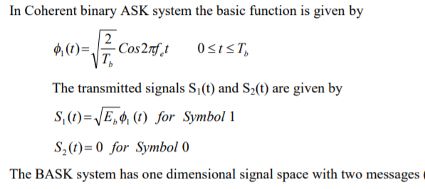
Fig 22 PSD for BFSK
BPSK
The low pass filter (LPF) is a filter “matched” to the baseband signal being transmitted. For BPSK this is just a rectangular pulse of duration T.
The impulse response is
H(t) = pr(t)
The output of the low pass filter is
X(t) = 
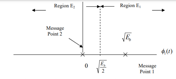
Fig 23 The output of LPF
The sampled version of the output is given by
Xi(t) = 
= 
= 
η is Gaussian random variable, mean 0 variance No/2.
Assuming 2π fcT =2πn for some integer n (or that fcT>> 1)
X(iT) = √PT bi-1 + 𝛈
Pe,b = Q (√2E /N0)
Where Q (x) = (1/2π) e –u2/2 du
For binary signals this is the smallest bit error probability, i.e. BPSK are optimal signals and the receiver shown above is optimum (in additive white Gaussian noise). For binary signals the energy transmitted per information bit Eb is equal to the energy per signal E.
For Pe b = 10-5 we need a bit-energy, Eb to noise density N0 ratio of Eb/N0 = 9.6dB.
Key takeaway

For Gray encoding,  can directly be computed.
Assume that  is transmitted which corresponds to
  Then the conditional bit error probability is given by


From the direct decision rule for data bits

 2=1⇔Y∈D2⋃D3
Thus,


By symmetry all conditional four bit errors probabilities are identical. Since two data bits are transmitted per modulation symbol (waveform) in QPSK, we have the relations  . Therefore,


Key takeaway
Since two data bits are transmitted per modulation symbol (waveform) in QPSK, we have the relations  . Therefore,

References
1. “Communication Systems”, Simon Haykin, Wiley publication, 4th Edition, 2004
2. “Digital Communication Fundamentals and Applications”, Bernard Sklar, Pearson
Education India, 2nd Edition, 2009
3. “Modern Electronic Communication”, Miller Gary M, Prentice-Hall, 6th Edition, 1999
4. “Digital Communications”, John Proakis, Tata Mc Graw Hill, 5th Edition, 2007
5. “Electronic Communication Systems, Fundamentals Through Advanced”, Wayne Tomsi, Pearson Education, 4th Edition, 2001
