Unit -3
Sequential circuits and systems
A latch is a simple digital circuit where the output can be set to either logic 1 or logic 0 by an input signal. The circuit then remains in this state even after the input is removed. This is a memory circuit that can “remember” a single binary digit (bit).
- In digital electronics, a Latch is one kind of a logic circuit, and it is also known as a bistable-multivibrator. Because it has two stable states namely active high as well as active low.
- It works like a storage device by holding the data through a feedback lane.
- It stores 1-bit of data as long as the apparatus is activated. Once enable is declared then instantly latch can change the stored data. It constantly trials the inputs once enable signal is activated.
- The working of these circuits can be done in 2-states based on the enable signal being high or else low. When the latch circuit is the in an active high state, then both the i/ps are low. Similarly, when the latch circuit is then an active low state, then both the i/ps are high.
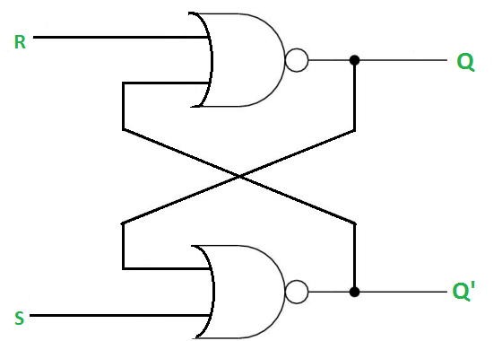
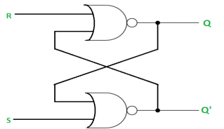
SR Latch is a circuit which has:
(i) 2 cross-coupled NOR gate or NAND gate.
(ii) 2 input S for SET and R for RESET.
(iii) 2 output Q and Q’.
Q | Q’ | STATE |
1 | 0 | Set |
0 | 1 | Reset |
Under normal conditions, both the input remains 0.
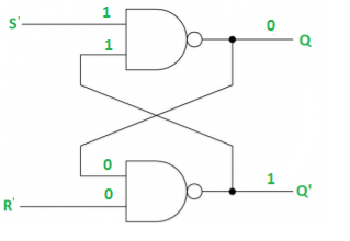
RS Latch with NAND gates:
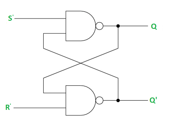
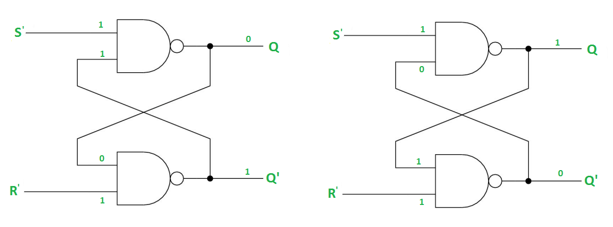
Case-1: When S’=R’=1 or S=R=0 then
If Q = 1, Q = R’ = 1.
If Q = 0, Q = 0 and R’ = 1 respectively.
Case-2: S’=0, R’=1 (S=1, R=0)
As S’=0, Q = 1(SET state).
In 2nd NAND gate, as Q = R’ = 1, Q’=0.
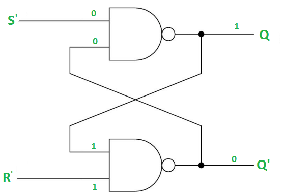
Case-3: S’= 1, R’= 0 (S=0, R=1)
As R’=0, Q’ = 1.
In 1st NAND gate, as Q =S’ = 1, Q=0 (RESET state).
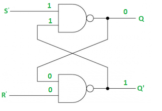
Case-4: S’= R’= 0 (S=R=1)
When S=R=1, both Q = Q’ = 1 which is not allowed.
So, this input condition is prohibited.
The SR Latch using NOR gate is:
Gated SR Latch –
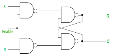
It is a latch which enable input that works when enable = 1 and retain the previous state when enable = 0.

Gated D Latch –
It is similar to SR latch with little modifications. Here, the inputs are complements of one another. The design of D latch with Enable signal is given below:

The truth table is shown below:
ENABLE | D | Q(N) | Q(N+1) | STATE |
1 | 0 | x | 0 | RESET |
1 | 1 | x | 1 | SET |
0 | x | x | Q(n) | No Change |
As the output is same as input, it is also known as Transparent Latch.
The characteristic equation for D latch with enable input is given as:
Q(n+1) = EN.D + EN'.Q(n)
J-K Flip Flop:

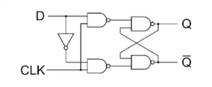
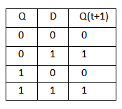
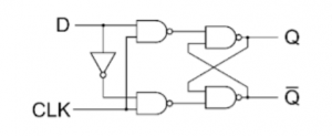
D Flip Flop
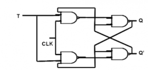
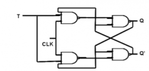
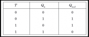
T Flip Flop :
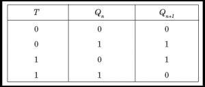
- When the clock pulse goes high, the slave is isolated; J and K inputs can affect the state of the system. The slave flip-flop is isolated when the CP goes low. When the CP goes back to 0, information is transmitted from the master flip-flop to the slave flip-flop and output is obtained.
- The master flip flop is positive level triggered and the slave flip flop is negative level triggered, hence the master responds prior to the slave.
- If J=0 and K=1, Q’ = 1 then the master goes to the K input of the slave and the clock forces the slave to reset therefore the slave copies the master.
- If J=1 and K=0, Q = 1 then the master goes to the J input of the slave and the Negative transition of the clock sets the slave and thus copy the master.
- If J=1 and K=1, the master toggles on the positive transition and the slave toggles on the negative transition of the clock.
- If J=0 and K=0, the flip flop becomes disabled and Q remains unchanged.
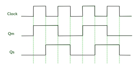
Timing Diagram of a Master flip flop –
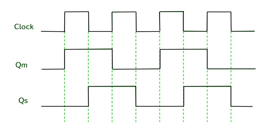
- When the CP = 1 then the output of master is high and remains high till CP = 0 because the state is stored.
- Now the output of master becomes low when the clock CP = 1 and remains low until the clock becomes high again.
- Thus toggling takes place for a clock cycle.
- When the CP = 1 then the master is operational but not the slave.
- When the clock is low, the slave becomes operational and remains high until the clock again becomes low.
- Toggling takes place during the whole process since the output changes once in a cycle.
- This makes the Master-Slave J-K flip flop a Synchronous device which passes data with the clock signal.
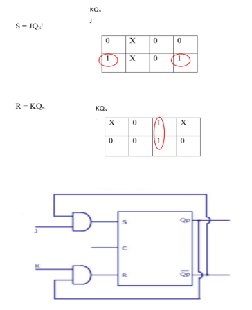
Conversion for FlipFlops :-
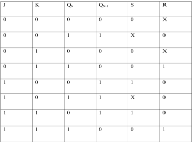
EXCITATION TABLE:
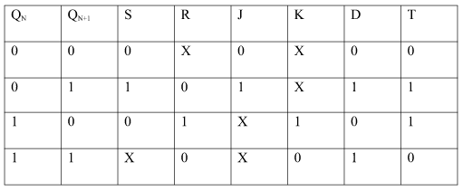
i) SR To JK FlipFlop
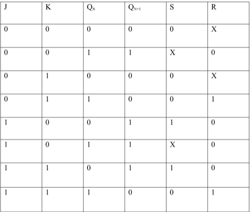
Excitation Functions:
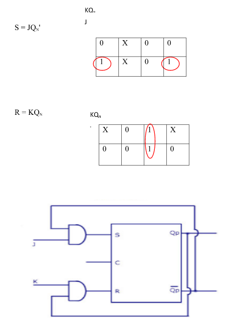
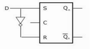
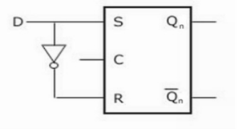
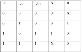
Ii) Convert SR To D FlipFlop:
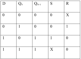
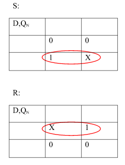
Excitation Functions:
S = D
R = D‘
- Flip flops are used to store one bit of binary data (1or 0).
- If we need to store multiple bits of data, we use multiple flip flops.
- N flip flops are connected to store n bits of data.
- A Register is a device which stores such information. It is a group of flip flops connected in series which is used to store multiple bits of data.
- The information stored in these registers can be transferred with the help of shift registers.
- This register is a group of flip flops used to store multiple bits of data.
- The bits stored in these registers can be moved in/out of the registers by applying clock pulses.
- The registers which shift the bits towards left are called “Shift left registers”.
The registers which shift the bits towards right are called “Shift right registers”.
Shift registers are of 4 types and they are:
- Serial In Serial Out register
- Serial In parallel Out register
- Parallel In Serial Out register
- Parallel In parallel Out register
- They are used for temporary data storage.
- They are used for data transfer and data manipulation.
- The SISO and PIPO registers are used to produce time delay in digital circuits.
- The SIPO register is used for conversion of serial data to parallel data hence they are used in communication lines .
- A PISO register is used to convert parallel data to serial data.
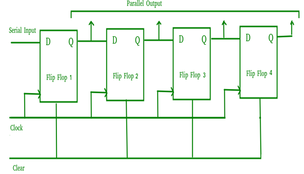
- It allows serial input through a single data line and produces a parallel output.
- The logic circuit is given underneath .
- The circuit consists of four D flip-flops which are connected synchronously.
- The clear (CLR) signal is also connected to all the 4 flip flops in order to RESET them.
- The output of the first flip flop is sent to the input of the next and so on.
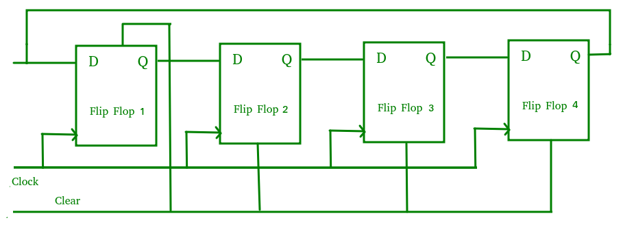
- It is a shift register counter whose output of the first flip flop is connected to the second and so on and the output of the last flip flop is fed back to the input of the first flip flop, thus named as ring counter.
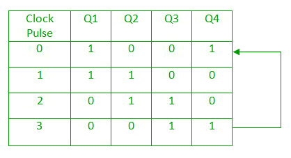
- The data pattern in the register circulates as long as clock pulses are applied.
- The circuit below comprises of four D flip-flops which are connected synchronously.
- The data pattern repeats after every four clock pulses shown in the truth table.
Ring counter
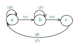
- It is a sequential state machine which takes an input string of bits and generates an output 1 whenever the target sequence has been detected.
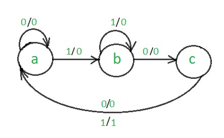
- In a Mealy machine, output depends on the present state and the external input (x).
- Hence the output is written outside the states, along with inputs.
- Sequence detector is of two types:
- Overlapping
- Non-Overlapping
- In an overlapping sequence detector the last bit of a sequence becomes the first bit of next one.
- In non-overlapping sequence detector the last bit of one sequence does not become the first bit of next one.
- Examples:
For non overlapping case
Input :0110101011001
Output:0000100010000
For overlapping case
Input :0110101011001
Output:0000101010000
The steps to design non-overlapping 101 Mealy sequence detector are:
Step 1: Development of the state diagram –
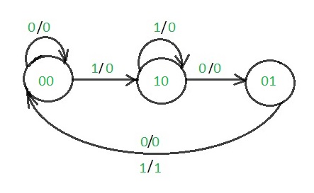
The state diagram of a Mealy machine for a 101 sequence detector is:
Step 2: Assignment of the code–
Rule 1 : States having the same next states for a given input condition should have adjacent assignments.
Rule 2:States that are the next states to a single state must be given adjacent assignments.
Rule 1 given preference over Rule 2.
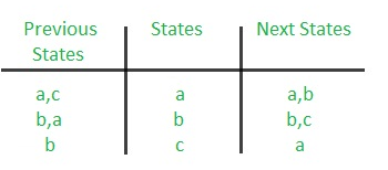

The state diagram after the code assignment is:
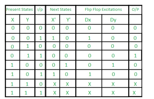
Step 3: Making Present State/Next State table –
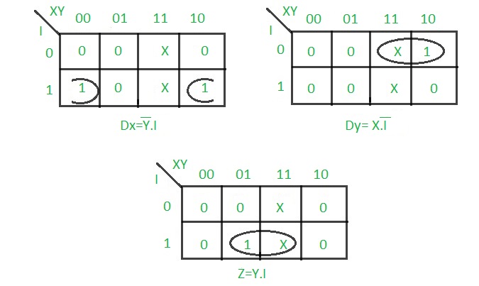
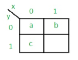
Step 4: Draw K-maps for Dx, Dy and output (Z) –
Step 5: Final implementation of the circuit –
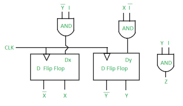
This is the desired circuit for a Mealy 101 non overlapping sequence detector.
- In this universal clock is not used and only the first flip flop is driven by main clock and the clock input of rest of the following is driven by output of previous flip flops.

Asynchronous counter

Timing diagram of Asynchronous counter
- It is seen from timing diagram that Q0 is changing as soon as the rising edge of clock pulse is encountered.
- Q1 is changing when rising edge of Q0 is encountered and so on.
- In this way ripples are generated through Q0,Q1,Q2,Q3 and therefore it is also called as a RIPPLE counter.
- It has one global clock which drives each and every flip flop and hence output changes in parallel.
- The advantage of synchronous counter over asynchronous counter is that it can operate on higher frequency and it does not have cumulative delay .
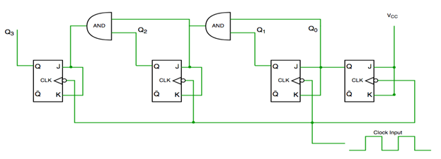
Synchronous counter
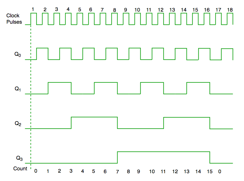
Timing diagram of synchronous counter
- A ripple counter is also called as an asynchronous counter. Here only the first flip-flop is clocked by an external clock and all subsequent flip-flops are clocked by the output of the preceding one.
- The MOD of the ripple counter is 2n where n is the no. Of flip-flops used.
- For example, a 4-bit counter, the range of the count is 0000 to 1111 i.e. (24-1).
- A counter may count up or down or up and down depending on the input control. The count sequence will repeat itself.
- There are many ways to implement the ripple counter which depends on the characteristics of the flip flops used and the requirements of the count sequence.
- Clock Trigger: Positive edged or Negative edged
- JK or D flip-flops
- Count Direction: Up, Down, or Up/Down
Asynchronous (Ripple) Counters:
- 74HC390 - Dual decade ripple counter from NXP.
- 74HC393 - Dual 4-stage binary ripple counter from ON Semiconductor.
- 74HC4040 - 12-Stage binary ripple counter from Fairchild Semiconductor.
- 74HC93 - 4-Bit binary ripple counter from Texas Instruments.
- CD4060 - 14-Stage binary counter plus oscillator from ST Microelectronics.
- HEF4042B - 7-Stage binary ripple counter from NXP.
Synchronous Counters:
- 74HC160 - Pre-settable synchronous BCD counter with asynchronous reset from NXP.
- 74HC161 - 4-Bit synchronous BCD counter with asynchronous reset and synchronous load from Texas Instruments.
- 74HC163 - 4-Bit synchronous binary counter with asynchronous reset and synchronous load from Texas Instruments.
- 74HC191 - 4-bit synchronous binary up/down counter with asynchronous reset and load from NXP.
- 74HC192 - 4-Bit synchronous BCD counter with asynchronous reset and load from Texas Instruments.
- 74HC193 - 4-Bit synchronous binary counter with asynchronous reset and load from Texas Instruments.
- CD4017/4022B - 4-Stage synchronous counters with Decade (1 of 10) or Octal (1 of 8) outputs from Texas Instruments.
- In this universal clock is not used and only the first flip flop is driven by main clock and the clock input of rest of the following is driven by output of previous flip flops.

Asynchronous counter
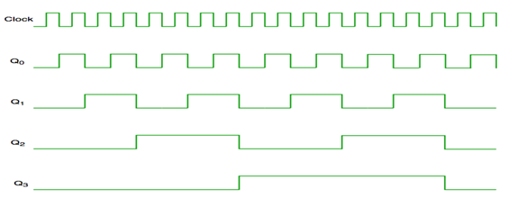
Timing diagram of Asynchronous counter
- It is seen from timing diagram that Q0 is changing as soon as the rising edge of clock pulse is encountered.
- Q1 is changing when rising edge of Q0 is encountered and so on.
In this way ripples are generated through Q0,Q1,Q2,Q3 and therefore it is also called as a RIPPLE counter.
- A Counter stores the number of times a particular event or process has occurred in relationship to a clock signal.
- They are used in digital electronics for counting purpose.
- They can count specific event happening how many times in the circuit.
- For example, in UP counter count increases for every rising edge of clock.
- A counter can follow certain sequence based on our design like any sequence 0,1,3,2… .
- They can be designed with the help of flip flops.
Reference
1. R. P. Jain, "Modern Digital Electronics", McGraw Hill Education, 2009.
2. M. M. Mano, "Digital logic and Computer design", Pearson Education India, 2016.
3. A. Kumar, "Fundamentals of Digital Circuits", Prentice Hall India, 2016.
Unit - 3
Sequential circuits and systems
A latch is a simple digital circuit where the output can be set to either logic 1 or logic 0 by an input signal. The circuit then remains in this state even after the input is removed. This is a memory circuit that can “remember” a single binary digit (bit).
- In digital electronics, a Latch is one kind of a logic circuit, and it is also known as a bistable-multivibrator. Because it has two stable states namely active high as well as active low.
- It works like a storage device by holding the data through a feedback lane.
- It stores 1-bit of data as long as the apparatus is activated. Once enable is declared then instantly latch can change the stored data. It constantly trials the inputs once enable signal is activated.
- The working of these circuits can be done in 2-states based on the enable signal being high or else low. When the latch circuit is the in an active high state, then both the i/ps are low. Similarly, when the latch circuit is then an active low state, then both the i/ps are high.
SR Latch is a circuit which has:
(i) 2 cross-coupled NOR gate or NAND gate.
(ii) 2 input S for SET and R for RESET.
(iii) 2 output Q and Q’.
Q | Q’ | STATE |
1 | 0 | Set |
0 | 1 | Reset |
Under normal conditions, both the input remains 0.
RS Latch with NAND gates:

Case-1: When S’=R’=1 or S=R=0 then
If Q = 1, Q = R’ = 1.
If Q = 0, Q = 0 and R’ = 1 respectively.

Case-2: S’=0, R’=1 (S=1, R=0)
As S’=0, Q = 1(SET state).
In 2nd NAND gate, as Q = R’ = 1, Q’=0.

Case-3: S’= 1, R’= 0 (S=0, R=1)
As R’=0, Q’ = 1.
In 1st NAND gate, as Q =S’ = 1, Q=0 (RESET state).

Case-4: S’= R’= 0 (S=R=1)
When S=R=1, both Q = Q’ = 1 which is not allowed.
So, this input condition is prohibited.
The SR Latch using NOR gate is:

Gated SR Latch –
It is a latch which enable input that works when enable = 1 and retain the previous state when enable = 0.
Gated D Latch –
It is similar to SR latch with little modifications. Here, the inputs are complements of one another. The design of D latch with Enable signal is given below:
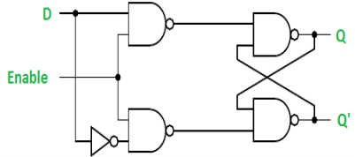
The truth table is shown below:
ENABLE | D | Q(N) | Q(N+1) | STATE |
1 | 0 | x | 0 | RESET |
1 | 1 | x | 1 | SET |
0 | x | x | Q(n) | No Change |
As the output is same as input, it is also known as Transparent Latch.
The characteristic equation for D latch with enable input is given as:
Q(n+1) = EN.D + EN'.Q(n)
J-K Flip Flop:

D Flip Flop

T Flip Flop:

- When the clock pulse goes high, the slave is isolated; J and K inputs can affect the state of the system. The slave flip-flop is isolated when the CP goes low. When the CP goes back to 0, information is transmitted from the master flip-flop to the slave flip-flop and output is obtained.
- The master flip flop is positive level triggered and the slave flip flop is negative level triggered, hence the master responds prior to the slave.
- If J=0 and K=1, Q’ = 1 then the master goes to the K input of the slave and the clock forces the slave to reset therefore the slave copies the master.
- If J=1 and K=0, Q = 1 then the master goes to the J input of the slave and the Negative transition of the clock sets the slave and thus copy the master.
- If J=1 and K=1, the master toggles on the positive transition and the slave toggles on the negative transition of the clock.
- If J=0 and K=0, the flip flop becomes disabled and Q remains unchanged.
Timing Diagram of a Master flip flop –

- When the CP = 1 then the output of master is high and remains high till CP = 0 because the state is stored.
- Now the output of master becomes low when the clock CP = 1 and remains low until the clock becomes high again.
- Thus toggling takes place for a clock cycle.
- When the CP = 1 then the master is operational but not the slave.
- When the clock is low, the slave becomes operational and remains high until the clock again becomes low.
- Toggling takes place during the whole process since the output changes once in a cycle.
- This makes the Master-Slave J-K flip flop a Synchronous device which passes data with the clock signal.
Conversion for Flip Flops:
EXCITATION TABLE:
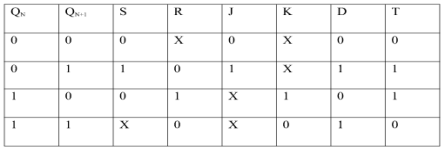
i) SR To JK FlipFlop

Excitation Functions:

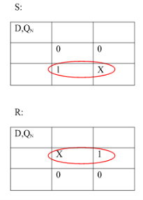
Ii) Convert SR To D Flip Flop:

Excitation Functions:
S = D
R = D‘

- Flip flops are used to store one bit of binary data (1or 0).
- If we need to store multiple bits of data, we use multiple flip flops.
- N flip flops are connected to store n bits of data.
- A Register is a device which stores such information. It is a group of flip flops connected in series which is used to store multiple bits of data.
- The information stored in these registers can be transferred with the help of shift registers.
- This register is a group of flip flops used to store multiple bits of data.
- The bits stored in these registers can be moved in/out of the registers by applying clock pulses.
- The registers which shift the bits towards left are called “Shift left registers”.
The registers which shift the bits towards right are called “Shift right registers”.
Shift registers are of 4 types and they are:
- Serial In Serial Out register
- Serial In parallel Out register
- Parallel In Serial Out register
- Parallel In parallel Out register
- They are used for temporary data storage.
- They are used for data transfer and data manipulation.
- The SISO and PIPO registers are used to produce time delay in digital circuits.
- The SIPO register is used for conversion of serial data to parallel data hence they are used in communication lines.
- A PISO register is used to convert parallel data to serial data.
- It allows serial input through a single data line and produces a parallel output.
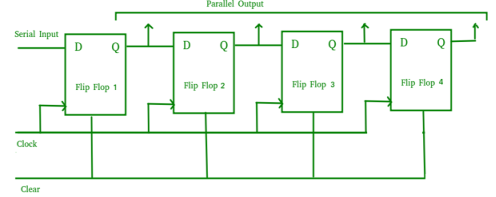
- The logic circuit is given underneath.
- The circuit consists of four D flip-flops which are connected synchronously.
- The clear (CLR) signal is also connected to all the 4 flip flops in order to RESET them.
- The output of the first flip flop is sent to the input of the next and so on.
- It is a shift register counter whose output of the first flip flop is connected to the second and so on and the output of the last flip flop is fed back to the input of the first flip flop, thus named as ring counter.
- The data pattern in the register circulates as long as clock pulses are applied.
- The circuit below comprises of four D flip-flops which are connected synchronously.
- The data pattern repeats after every four clock pulses shown in the truth table.
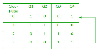

Fig. Ring counter
- It is a sequential state machine which takes an input string of bits and generates an output 1 whenever the target sequence has been detected.
- In a Mealy machine, output depends on the present state and the external input (x).
- Hence the output is written outside the states, along with inputs.
- Sequence detector is of two types:
- Overlapping
- Non-Overlapping
- In an overlapping sequence detector the last bit of a sequence becomes the first bit of next one.
- In non-overlapping sequence detector the last bit of one sequence does not become the first bit of next one.
- Examples:
For non overlapping case
Input :0110101011001
Output:0000100010000
For overlapping case
Input :0110101011001
Output:0000101010000
The steps to design non-overlapping 101 Mealy sequence detector are:
Step 1: Development of the state diagram –
The state diagram of a Mealy machine for a 101 sequence detector is:

Step 2: Assignment of the code–
Rule 1: States having the same next states for a given input condition should have adjacent assignments.
Rule 2: States that are the next states to a single state must be given adjacent assignments.
Rule 1 given preference over Rule 2.
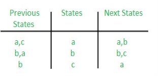

The state diagram after the code assignment is:

Step 3: Making Present State/Next State table –
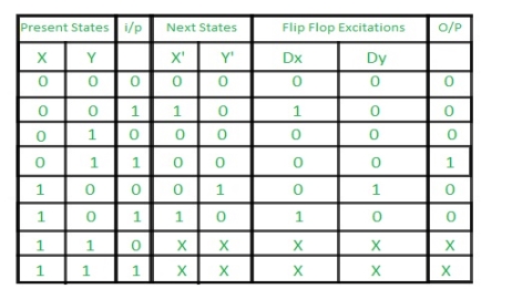
Step 4: Draw K-maps for Dx, Dy and output (Z) –

Step 5: Final implementation of the circuit –

This is the desired circuit for a Mealy 101 non overlapping sequence detector.
- In this universal clock is not used and only the first flip flop is driven by main clock and the clock input of rest of the following is driven by output of previous flip flops.

Fig. Asynchronous counter
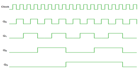
Fig. Timing diagram of Asynchronous counter
- It is seen from timing diagram that Q0 is changing as soon as the rising edge of clock pulse is encountered.
- Q1 is changing when rising edge of Q0 is encountered and so on.
- In this way ripples are generated through Q0,Q1,Q2,Q3 and therefore it is also called as a RIPPLE counter.
- It has one global clock which drives each and every flip flop and hence output changes in parallel.
- The advantage of synchronous counter over asynchronous counter is that it can operate on higher frequency and it does not have cumulative delay.

Fig. Synchronous counter

Fig. Timing diagram of synchronous counter
- A ripple counter is also called as an asynchronous counter. Here only the first flip-flop is clocked by an external clock and all subsequent flip-flops are clocked by the output of the preceding one.
- The MOD of the ripple counter is 2n where n is the no. Of flip-flops used.
- For example, a 4-bit counter, the range of the count is 0000 to 1111 i.e. (24-1).
- A counter may count up or down or up and down depending on the input control. The count sequence will repeat itself.
- There are many ways to implement the ripple counter which depends on the characteristics of the flip flops used and the requirements of the count sequence.
- Clock Trigger: Positive edged or Negative edged
- JK or D flip-flops
- Count Direction: Up, Down, or Up/Down
Asynchronous (Ripple) Counters:
- 74HC390 - Dual decade ripple counter from NXP.
- 74HC393 - Dual 4-stage binary ripple counter from ON Semiconductor.
- 74HC4040 - 12-Stage binary ripple counter from Fairchild Semiconductor.
- 74HC93 - 4-Bit binary ripple counter from Texas Instruments.
- CD4060 - 14-Stage binary counter plus oscillator from ST Microelectronics.
- HEF4042B - 7-Stage binary ripple counter from NXP.
Synchronous Counters:
- 74HC160 - Pre-settable synchronous BCD counter with asynchronous reset from NXP.
- 74HC161 - 4-Bit synchronous BCD counter with asynchronous reset and synchronous load from Texas Instruments.
- 74HC163 - 4-Bit synchronous binary counter with asynchronous reset and synchronous load from Texas Instruments.
- 74HC191 - 4-bit synchronous binary up/down counter with asynchronous reset and load from NXP.
- 74HC192 - 4-Bit synchronous BCD counter with asynchronous reset and load from Texas Instruments.
- 74HC193 - 4-Bit synchronous binary counter with asynchronous reset and load from Texas Instruments.
- CD4017/4022B - 4-Stage synchronous counters with Decade (1 of 10) or Octal (1 of 8) outputs from Texas Instruments.
Unit - 3
Sequential circuits and systems
A latch is a simple digital circuit where the output can be set to either logic 1 or logic 0 by an input signal. The circuit then remains in this state even after the input is removed. This is a memory circuit that can “remember” a single binary digit (bit).
- In digital electronics, a Latch is one kind of a logic circuit, and it is also known as a bistable-multivibrator. Because it has two stable states namely active high as well as active low.
- It works like a storage device by holding the data through a feedback lane.
- It stores 1-bit of data as long as the apparatus is activated. Once enable is declared then instantly latch can change the stored data. It constantly trials the inputs once enable signal is activated.
- The working of these circuits can be done in 2-states based on the enable signal being high or else low. When the latch circuit is the in an active high state, then both the i/ps are low. Similarly, when the latch circuit is then an active low state, then both the i/ps are high.
SR Latch is a circuit which has:
(i) 2 cross-coupled NOR gate or NAND gate.
(ii) 2 input S for SET and R for RESET.
(iii) 2 output Q and Q’.
Q | Q’ | STATE |
1 | 0 | Set |
0 | 1 | Reset |
Under normal conditions, both the input remains 0.
RS Latch with NAND gates:

Case-1: When S’=R’=1 or S=R=0 then
If Q = 1, Q = R’ = 1.
If Q = 0, Q = 0 and R’ = 1 respectively.
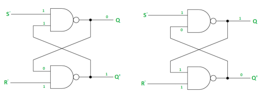
Case-2: S’=0, R’=1 (S=1, R=0)
As S’=0, Q = 1(SET state).
In 2nd NAND gate, as Q = R’ = 1, Q’=0.

Case-3: S’= 1, R’= 0 (S=0, R=1)
As R’=0, Q’ = 1.
In 1st NAND gate, as Q =S’ = 1, Q=0 (RESET state).
Case-4: S’= R’= 0 (S=R=1)
When S=R=1, both Q = Q’ = 1 which is not allowed.
So, this input condition is prohibited.
The SR Latch using NOR gate is:
Gated SR Latch –
It is a latch which enable input that works when enable = 1 and retain the previous state when enable = 0.

Gated D Latch –
It is similar to SR latch with little modifications. Here, the inputs are complements of one another. The design of D latch with Enable signal is given below:

The truth table is shown below:
ENABLE | D | Q(N) | Q(N+1) | STATE |
1 | 0 | x | 0 | RESET |
1 | 1 | x | 1 | SET |
0 | x | x | Q(n) | No Change |
As the output is same as input, it is also known as Transparent Latch.
The characteristic equation for D latch with enable input is given as:
Q(n+1) = EN.D + EN'.Q(n)
J-K Flip Flop:

D Flip Flop


T Flip Flop:


- When the clock pulse goes high, the slave is isolated; J and K inputs can affect the state of the system. The slave flip-flop is isolated when the CP goes low. When the CP goes back to 0, information is transmitted from the master flip-flop to the slave flip-flop and output is obtained.
- The master flip flop is positive level triggered and the slave flip flop is negative level triggered, hence the master responds prior to the slave.
- If J=0 and K=1, Q’ = 1 then the master goes to the K input of the slave and the clock forces the slave to reset therefore the slave copies the master.
- If J=1 and K=0, Q = 1 then the master goes to the J input of the slave and the Negative transition of the clock sets the slave and thus copy the master.
- If J=1 and K=1, the master toggles on the positive transition and the slave toggles on the negative transition of the clock.
- If J=0 and K=0, the flip flop becomes disabled and Q remains unchanged.
Timing Diagram of a Master flip flop –
- When the CP = 1 then the output of master is high and remains high till CP = 0 because the state is stored.
- Now the output of master becomes low when the clock CP = 1 and remains low until the clock becomes high again.
- Thus toggling takes place for a clock cycle.
- When the CP = 1 then the master is operational but not the slave.
- When the clock is low, the slave becomes operational and remains high until the clock again becomes low.
- Toggling takes place during the whole process since the output changes once in a cycle.
- This makes the Master-Slave J-K flip flop a Synchronous device which passes data with the clock signal.
Conversion for Flip Flops:
EXCITATION TABLE:

i) SR To JK FlipFlop

Excitation Functions:
Ii) Convert SR To D Flip Flop:

Excitation Functions:
S = D
R = D‘

- Flip flops are used to store one bit of binary data (1or 0).
- If we need to store multiple bits of data, we use multiple flip flops.
- N flip flops are connected to store n bits of data.
- A Register is a device which stores such information. It is a group of flip flops connected in series which is used to store multiple bits of data.
- The information stored in these registers can be transferred with the help of shift registers.
- This register is a group of flip flops used to store multiple bits of data.
- The bits stored in these registers can be moved in/out of the registers by applying clock pulses.
- The registers which shift the bits towards left are called “Shift left registers”.
The registers which shift the bits towards right are called “Shift right registers”.
Shift registers are of 4 types and they are:
- Serial In Serial Out register
- Serial In parallel Out register
- Parallel In Serial Out register
- Parallel In parallel Out register
- They are used for temporary data storage.
- They are used for data transfer and data manipulation.
- The SISO and PIPO registers are used to produce time delay in digital circuits.
- The SIPO register is used for conversion of serial data to parallel data hence they are used in communication lines.
- A PISO register is used to convert parallel data to serial data.
- It allows serial input through a single data line and produces a parallel output.
- The logic circuit is given underneath.
- The circuit consists of four D flip-flops which are connected synchronously.
- The clear (CLR) signal is also connected to all the 4 flip flops in order to RESET them.
- The output of the first flip flop is sent to the input of the next and so on.

- It is a shift register counter whose output of the first flip flop is connected to the second and so on and the output of the last flip flop is fed back to the input of the first flip flop, thus named as ring counter.
- The data pattern in the register circulates as long as clock pulses are applied.
- The circuit below comprises of four D flip-flops which are connected synchronously.
- The data pattern repeats after every four clock pulses shown in the truth table.


Fig. Ring counter
- It is a sequential state machine which takes an input string of bits and generates an output 1 whenever the target sequence has been detected.
- In a Mealy machine, output depends on the present state and the external input (x).
- Hence the output is written outside the states, along with inputs.
- Sequence detector is of two types:
- Overlapping
- Non-Overlapping
- In an overlapping sequence detector the last bit of a sequence becomes the first bit of next one.
- In non-overlapping sequence detector the last bit of one sequence does not become the first bit of next one.
- Examples:
For non overlapping case
Input :0110101011001
Output:0000100010000
For overlapping case
Input :0110101011001
Output:0000101010000
The steps to design non-overlapping 101 Mealy sequence detector are:
Step 1: Development of the state diagram –
The state diagram of a Mealy machine for a 101 sequence detector is:
Step 2: Assignment of the code–
Rule 1: States having the same next states for a given input condition should have adjacent assignments.
Rule 2: States that are the next states to a single state must be given adjacent assignments.
Rule 1 given preference over Rule 2.


The state diagram after the code assignment is:
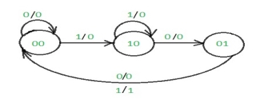
Step 3: Making Present State/Next State table –

Step 4: Draw K-maps for Dx, Dy and output (Z) –

Step 5: Final implementation of the circuit –

This is the desired circuit for a Mealy 101 non overlapping sequence detector.
- In this universal clock is not used and only the first flip flop is driven by main clock and the clock input of rest of the following is driven by output of previous flip flops.

Fig. Asynchronous counter

Fig. Timing diagram of Asynchronous counter
- It is seen from timing diagram that Q0 is changing as soon as the rising edge of clock pulse is encountered.
- Q1 is changing when rising edge of Q0 is encountered and so on.
- In this way ripples are generated through Q0,Q1,Q2,Q3 and therefore it is also called as a RIPPLE counter.
- It has one global clock which drives each and every flip flop and hence output changes in parallel.
- The advantage of synchronous counter over asynchronous counter is that it can operate on higher frequency and it does not have cumulative delay.
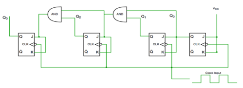
Fig. Synchronous counter

Fig. Timing diagram of synchronous counter
- A ripple counter is also called as an asynchronous counter. Here only the first flip-flop is clocked by an external clock and all subsequent flip-flops are clocked by the output of the preceding one.
- The MOD of the ripple counter is 2n where n is the no. Of flip-flops used.
- For example, a 4-bit counter, the range of the count is 0000 to 1111 i.e. (24-1).
- A counter may count up or down or up and down depending on the input control. The count sequence will repeat itself.
- There are many ways to implement the ripple counter which depends on the characteristics of the flip flops used and the requirements of the count sequence.
- Clock Trigger: Positive edged or Negative edged
- JK or D flip-flops
- Count Direction: Up, Down, or Up/Down
Asynchronous (Ripple) Counters:
- 74HC390 - Dual decade ripple counter from NXP.
- 74HC393 - Dual 4-stage binary ripple counter from ON Semiconductor.
- 74HC4040 - 12-Stage binary ripple counter from Fairchild Semiconductor.
- 74HC93 - 4-Bit binary ripple counter from Texas Instruments.
- CD4060 - 14-Stage binary counter plus oscillator from ST Microelectronics.
- HEF4042B - 7-Stage binary ripple counter from NXP.
Synchronous Counters:
- 74HC160 - Pre-settable synchronous BCD counter with asynchronous reset from NXP.
- 74HC161 - 4-Bit synchronous BCD counter with asynchronous reset and synchronous load from Texas Instruments.
- 74HC163 - 4-Bit synchronous binary counter with asynchronous reset and synchronous load from Texas Instruments.
- 74HC191 - 4-bit synchronous binary up/down counter with asynchronous reset and load from NXP.
- 74HC192 - 4-Bit synchronous BCD counter with asynchronous reset and load from Texas Instruments.
- 74HC193 - 4-Bit synchronous binary counter with asynchronous reset and load from Texas Instruments.
- CD4017/4022B - 4-Stage synchronous counters with Decade (1 of 10) or Octal (1 of 8) outputs from Texas Instruments.
- In this universal clock is not used and only the first flip flop is driven by main clock and the clock input of rest of the following is driven by output of previous flip flops.

Fig. Asynchronous counter

Fig. Timing diagram of Asynchronous counter
- It is seen from timing diagram that Q0 is changing as soon as the rising edge of clock pulse is encountered.
- Q1 is changing when rising edge of Q0 is encountered and so on.
In this way ripples are generated through Q0,Q1,Q2,Q3 and therefore it is also called as a RIPPLE counter.
- A Counter stores the number of times a particular event or process has occurred in relationship to a clock signal.
- They are used in digital electronics for counting purpose.
- They can count specific event happening how many times in the circuit.
- For example, in UP counter count increases for every rising edge of clock.
- A counter can follow certain sequence based on our design like any sequence 0,1,3,2… .
- They can be designed with the help of flip flops.
References:
1. R. P. Jain, "Modern Digital Electronics", McGraw Hill Education, 2009.
2. M. M. Mano, "Digital logic and Computer design", Pearson Education India, 2016.
3. A. Kumar, "Fundamentals of Digital Circuits", Prentice Hall India, 2016.
Unit - 3
Sequential circuits and systems
A latch is a simple digital circuit where the output can be set to either logic 1 or logic 0 by an input signal. The circuit then remains in this state even after the input is removed. This is a memory circuit that can “remember” a single binary digit (bit).
- In digital electronics, a Latch is one kind of a logic circuit, and it is also known as a bistable-multivibrator. Because it has two stable states namely active high as well as active low.
- It works like a storage device by holding the data through a feedback lane.
- It stores 1-bit of data as long as the apparatus is activated. Once enable is declared then instantly latch can change the stored data. It constantly trials the inputs once enable signal is activated.
- The working of these circuits can be done in 2-states based on the enable signal being high or else low. When the latch circuit is the in an active high state, then both the i/ps are low. Similarly, when the latch circuit is then an active low state, then both the i/ps are high.
SR Latch is a circuit which has:
(i) 2 cross-coupled NOR gate or NAND gate.
(ii) 2 input S for SET and R for RESET.
(iii) 2 output Q and Q’.
Q | Q’ | STATE |
1 | 0 | Set |
0 | 1 | Reset |
Under normal conditions, both the input remains 0.
RS Latch with NAND gates:
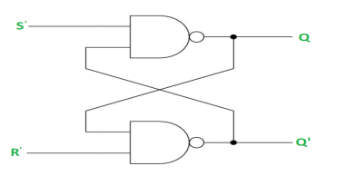
Case-1: When S’=R’=1 or S=R=0 then
If Q = 1, Q = R’ = 1.
If Q = 0, Q = 0 and R’ = 1 respectively.

Case-2: S’=0, R’=1 (S=1, R=0)
As S’=0, Q = 1(SET state).
In 2nd NAND gate, as Q = R’ = 1, Q’=0.
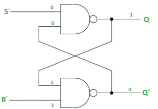
Case-3: S’= 1, R’= 0 (S=0, R=1)
As R’=0, Q’ = 1.
In 1st NAND gate, as Q =S’ = 1, Q=0 (RESET state).

Case-4: S’= R’= 0 (S=R=1)
When S=R=1, both Q = Q’ = 1 which is not allowed.
So, this input condition is prohibited.
The SR Latch using NOR gate is:

Gated SR Latch –
It is a latch which enable input that works when enable = 1 and retain the previous state when enable = 0.

Gated D Latch –
It is similar to SR latch with little modifications. Here, the inputs are complements of one another. The design of D latch with Enable signal is given below:

The truth table is shown below:
ENABLE | D | Q(N) | Q(N+1) | STATE |
1 | 0 | x | 0 | RESET |
1 | 1 | x | 1 | SET |
0 | x | x | Q(n) | No Change |
As the output is same as input, it is also known as Transparent Latch.
The characteristic equation for D latch with enable input is given as:
Q(n+1) = EN.D + EN'.Q(n)
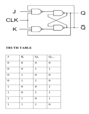
J-K Flip Flop:
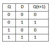
D Flip Flop

T Flip Flop:

- When the clock pulse goes high, the slave is isolated; J and K inputs can affect the state of the system. The slave flip-flop is isolated when the CP goes low. When the CP goes back to 0, information is transmitted from the master flip-flop to the slave flip-flop and output is obtained.
- The master flip flop is positive level triggered and the slave flip flop is negative level triggered, hence the master responds prior to the slave.
- If J=0 and K=1, Q’ = 1 then the master goes to the K input of the slave and the clock forces the slave to reset therefore the slave copies the master.
- If J=1 and K=0, Q = 1 then the master goes to the J input of the slave and the Negative transition of the clock sets the slave and thus copy the master.
- If J=1 and K=1, the master toggles on the positive transition and the slave toggles on the negative transition of the clock.
- If J=0 and K=0, the flip flop becomes disabled and Q remains unchanged.
Timing Diagram of a Master flip flop –

- When the CP = 1 then the output of master is high and remains high till CP = 0 because the state is stored.
- Now the output of master becomes low when the clock CP = 1 and remains low until the clock becomes high again.
- Thus toggling takes place for a clock cycle.
- When the CP = 1 then the master is operational but not the slave.
- When the clock is low, the slave becomes operational and remains high until the clock again becomes low.
- Toggling takes place during the whole process since the output changes once in a cycle.
- This makes the Master-Slave J-K flip flop a Synchronous device which passes data with the clock signal.
Conversion for Flip Flops:
EXCITATION TABLE:

i) SR To JK FlipFlop
Excitation Functions:

Ii) Convert SR To D Flip Flop:
Excitation Functions:
S = D
R = D‘


- Flip flops are used to store one bit of binary data (1or 0).
- If we need to store multiple bits of data, we use multiple flip flops.
- N flip flops are connected to store n bits of data.
- A Register is a device which stores such information. It is a group of flip flops connected in series which is used to store multiple bits of data.
- The information stored in these registers can be transferred with the help of shift registers.
- This register is a group of flip flops used to store multiple bits of data.
- The bits stored in these registers can be moved in/out of the registers by applying clock pulses.
- The registers which shift the bits towards left are called “Shift left registers”.
The registers which shift the bits towards right are called “Shift right registers”.
Shift registers are of 4 types and they are:
- Serial In Serial Out register
- Serial In parallel Out register
- Parallel In Serial Out register
- Parallel In parallel Out register
- They are used for temporary data storage.
- They are used for data transfer and data manipulation.
- The SISO and PIPO registers are used to produce time delay in digital circuits.
- The SIPO register is used for conversion of serial data to parallel data hence they are used in communication lines.
- A PISO register is used to convert parallel data to serial data.
- It allows serial input through a single data line and produces a parallel output.
- The logic circuit is given underneath.
- The circuit consists of four D flip-flops which are connected synchronously.
- The clear (CLR) signal is also connected to all the 4 flip flops in order to RESET them.
- The output of the first flip flop is sent to the input of the next and so on.

- It is a shift register counter whose output of the first flip flop is connected to the second and so on and the output of the last flip flop is fed back to the input of the first flip flop, thus named as ring counter.
- The data pattern in the register circulates as long as clock pulses are applied.
- The circuit below comprises of four D flip-flops which are connected synchronously.
- The data pattern repeats after every four clock pulses shown in the truth table.


Fig. Ring counter
- It is a sequential state machine which takes an input string of bits and generates an output 1 whenever the target sequence has been detected.
- In a Mealy machine, output depends on the present state and the external input (x).
- Hence the output is written outside the states, along with inputs.
- Sequence detector is of two types:
- Overlapping
- Non-Overlapping
- In an overlapping sequence detector the last bit of a sequence becomes the first bit of next one.
- In non-overlapping sequence detector the last bit of one sequence does not become the first bit of next one.
- Examples:
For non overlapping case
Input :0110101011001
Output:0000100010000
For overlapping case
Input :0110101011001
Output:0000101010000
The steps to design non-overlapping 101 Mealy sequence detector are:
Step 1: Development of the state diagram –
The state diagram of a Mealy machine for a 101 sequence detector is:

Step 2: Assignment of the code–
Rule 1: States having the same next states for a given input condition should have adjacent assignments.
Rule 2: States that are the next states to a single state must be given adjacent assignments.
Rule 1 given preference over Rule 2.

The state diagram after the code assignment is:

Step 3: Making Present State/Next State table –

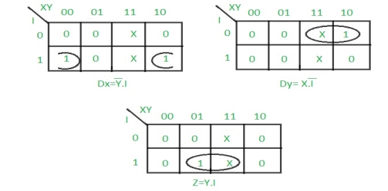
Step 4: Draw K-maps for Dx, Dy and output (Z) –
Step 5: Final implementation of the circuit –
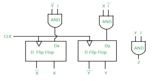
This is the desired circuit for a Mealy 101 non overlapping sequence detector.
- In this universal clock is not used and only the first flip flop is driven by main clock and the clock input of rest of the following is driven by output of previous flip flops.

Fig. Asynchronous counter

Fig. Timing diagram of Asynchronous counter
- It is seen from timing diagram that Q0 is changing as soon as the rising edge of clock pulse is encountered.
- Q1 is changing when rising edge of Q0 is encountered and so on.
- In this way ripples are generated through Q0,Q1,Q2,Q3 and therefore it is also called as a RIPPLE counter.
- It has one global clock which drives each and every flip flop and hence output changes in parallel.
- The advantage of synchronous counter over asynchronous counter is that it can operate on higher frequency and it does not have cumulative delay.

Fig. Synchronous counter
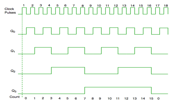
Fig. Timing diagram of synchronous counter
- A ripple counter is also called as an asynchronous counter. Here only the first flip-flop is clocked by an external clock and all subsequent flip-flops are clocked by the output of the preceding one.
- The MOD of the ripple counter is 2n where n is the no. Of flip-flops used.
- For example, a 4-bit counter, the range of the count is 0000 to 1111 i.e. (24-1).
- A counter may count up or down or up and down depending on the input control. The count sequence will repeat itself.
- There are many ways to implement the ripple counter which depends on the characteristics of the flip flops used and the requirements of the count sequence.
- Clock Trigger: Positive edged or Negative edged
- JK or D flip-flops
- Count Direction: Up, Down, or Up/Down
Asynchronous (Ripple) Counters:
- 74HC390 - Dual decade ripple counter from NXP.
- 74HC393 - Dual 4-stage binary ripple counter from ON Semiconductor.
- 74HC4040 - 12-Stage binary ripple counter from Fairchild Semiconductor.
- 74HC93 - 4-Bit binary ripple counter from Texas Instruments.
- CD4060 - 14-Stage binary counter plus oscillator from ST Microelectronics.
- HEF4042B - 7-Stage binary ripple counter from NXP.
Synchronous Counters:
- 74HC160 - Pre-settable synchronous BCD counter with asynchronous reset from NXP.
- 74HC161 - 4-Bit synchronous BCD counter with asynchronous reset and synchronous load from Texas Instruments.
- 74HC163 - 4-Bit synchronous binary counter with asynchronous reset and synchronous load from Texas Instruments.
- 74HC191 - 4-bit synchronous binary up/down counter with asynchronous reset and load from NXP.
- 74HC192 - 4-Bit synchronous BCD counter with asynchronous reset and load from Texas Instruments.
- 74HC193 - 4-Bit synchronous binary counter with asynchronous reset and load from Texas Instruments.
- CD4017/4022B - 4-Stage synchronous counters with Decade (1 of 10) or Octal (1 of 8) outputs from Texas Instruments.
- In this universal clock is not used and only the first flip flop is driven by main clock and the clock input of rest of the following is driven by output of previous flip flops.
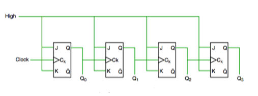
Fig. Asynchronous counter
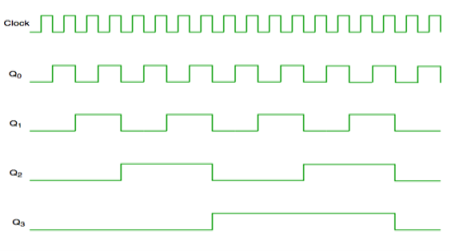
Fig. Timing diagram of Asynchronous counter
- It is seen from timing diagram that Q0 is changing as soon as the rising edge of clock pulse is encountered.
- Q1 is changing when rising edge of Q0 is encountered and so on.
In this way ripples are generated through Q0,Q1,Q2,Q3 and therefore it is also called as a RIPPLE counter.
- A Counter stores the number of times a particular event or process has occurred in relationship to a clock signal.
- They are used in digital electronics for counting purpose.
- They can count specific event happening how many times in the circuit.
- For example, in UP counter count increases for every rising edge of clock.
- A counter can follow certain sequence based on our design like any sequence 0,1,3,2… .
- They can be designed with the help of flip flops.
References:
1. R. P. Jain, "Modern Digital Electronics", McGraw Hill Education, 2009.
2. M. M. Mano, "Digital logic and Computer design", Pearson Education India, 2016.
3. A. Kumar, "Fundamentals of Digital Circuits", Prentice Hall India, 2016.