UNIT-1
Functional blocks of a computer, Data representation
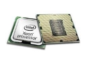
A Central Processing Unit is also called a processor, central processor, or microprocessor. It carries out all the important functions of a computer. It receives instructions from both the hardware and active software and produces output accordingly. It stores all important programs like operating systems and application software. CPU also helps Input and output devices to communicate with each other. Owing to these features of CPU, it is often referred to as the brain of the computer.
CPU is installed or inserted into a CPU socket located on the motherboard. Furthermore, it is provided with a heat sink to absorb and dissipate heat to keep the CPU cool and functioning smoothly.
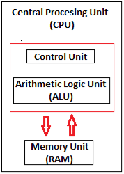
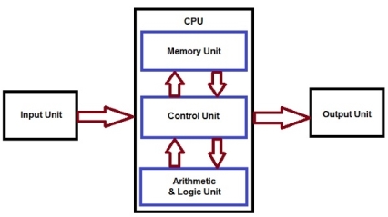
Generally, a CPU has three components:
- ALU (Arithmetic Logic Unit)
- Control Unit
- Memory or Storage Unit
|
Fig 1 - CPU
Control Unit: It is the circuitry in the control unit, which makes use of electrical signals to instruct the computer system for executing already stored instructions. It takes instructions from memory and then decodes and executes these instructions. So, it controls and coordinates the functioning of all parts of the computer. The Control Unit's main task is to maintain and regulate the flow of information across the processor. It does not take part in processing and storing data.
ALU: It is the arithmetic logic unit, which performs arithmetic and logical functions. Arithmetic functions include addition, subtraction, multiplication division, and comparisons. Logical functions mainly include selecting, comparing, and merging the data. A CPU may contain more than one ALU. Furthermore, ALUs can be used for maintaining timers that help run the computer.
Memory or Storage Unit/ Registers: It is called Random access memory (RAM). It temporarily stores data, programs, and intermediate and final results of processing. So, it acts as a temporary storage area that holds the data temporarily, which is used to run the computer.
The clock speed of a CPU or a processor refers to the number of instructions it can process in a second. It is measured in gigahertz. For example, a CPU with a clock speed of 4.0 GHz means it can process 4 billion instructions in a second.
CPUs are mostly manufactured by Intel and AMD, each of which manufactures its own types of CPUs. In modern times, there are lots of CPU types in the market. Some of the basic types of CPUs are described below:
Single Core CPU: Single Core is the oldest type of computer CPU, which was used in the 1970s. It has only one core to process different operations. It can start only one operation at a time; the CPU switches back and forth between different sets of data streams when more than one program runs. So, it is not suitable for multitasking as the performance will be reduced if more than one application runs. The performance of these CPUs is mainly dependent on the clock speed. It is still used in various devices, such as smartphones.
Dual Core CPU: As the name suggests, Dual Core CPU contains two cores in a single Integrated Circuit (IC). Although each core has its own controller and cache, they are linked together to work as a single unit and thus can perform faster than the single-core processors and can handle multitasking more efficiently than Single Core processors.
Quad Core CPU: This type of CPU comes with two dual-core processors in one integrated circuit (IC) or chip. So, a quad-core processor is a chip that contains four independent units called cores. These cores read and execute instructions of CPU. The cores can run multiple instructions simultaneously, thereby increases the overall speed for programs that are compatible with parallel processing.
Quad Core CPU uses a technology that allows four independent processing units (cores) to run in parallel on a single chip. Thus by integrating multiple cores in a single CPU, higher performance can be generated without boosting the clock speed. However, the performance increases only when the computer's software supports multiprocessing. The software which supports multiprocessing divides the processing load between multiple processors instead of using one processor at a time.
Some of the important events in the development of CPU since its invention till date are as follows:
- In 1823, Baron Jons Jackob Berzelius discovered silicon that is the main component of CPU till date.
- In 1903, Nikola Tesla got gates or switches patented, which are electrical logic circuits.
- In December 1947, John Bardeen, William Shockley, and Walter Brattain invented the first transistor at the Bell Laboratories and got it patented in 1948.
- In 1958, the first working integrated circuit was developed by Robert Noyce and Jack Kilby.
- In 1960, IBM established the first mass-production facility for transistors in New York.
- In 1968, Robert Noyce and Gordon Moore founded Intel Corporation.
- AMD (Advanced Micro Devices) was founded in May 1969.
- In 1971, Intel introduced the first microprocessor, the Intel 4004, with the help of Ted Hoff.
- In 1972, Intel introduced the 8008 processor; in 1976, Intel 8086 was introduced, and in June 1979, Intel 8088 was released.
- In 1979, a 16/32-bit processor, the Motorola 68000, was released. Later, it was used as a processor for the Apple Macintosh and Amiga computers.
- In 1987, Sun introduced the SPARC processor.
- In March 1991, AMD introduced the AM386 microprocessor family.
- In March 1993, Intel released the Pentium processor. In 1995, Cyrix introduced the Cx5x86 processor to give competition to Intel Pentium processors.
- In January 1999, Intel introduced the Celeron 366 MHz and 400 MHz processors.
- In April 2005, AMD introduced its first dual-core processor.
- In 2006, Intel introduced the Core 2 Duo processor.
- In 2007, Intel introduced different types of Core 2 Quad processors.
- In April 2008, Intel introduced the first series of Intel Atom processors, the Z5xx series. They were single-core processors with a 200 MHz GPU.
- In September 2009, Intel released the first Core i5 desktop processor with four cores.
- In January 2010, Intel released many processors such as Core 2 Quad processor Q9500, first Core i3 and i5 mobile processors, first Core i3 and i5 desktop processors. In the same year in July, it released the first Core i7 desktop processor with six cores.
- In June 2017, Intel introduced the first Core i9 desktop processor.
- In April 2018, Intel released the first Core i9 mobile processor.
The computer memory holds the data and instructions needed to process raw data and produce output. The computer memory is divided into large number of small parts known as cells. Each cell has a unique address which varies from 0 to memory size minus one.
Computer memory is of two types: Volatile (RAM) and Non-volatile (ROM). The secondary memory (hard disk) is referred as storage not memory.
But, if we categorize memory on behalf of space or location, it is of four types:
- Register memory
- Cache memory
- Primary memory
- Secondary memory
Register memory is the smallest and fastest memory in a computer. It is not a part of the main memory and is located in the CPU in the form of registers, which are the smallest data holding elements. A register temporarily holds frequently used data, instructions, and memory address that are to be used by CPU. They hold instructions that are currently processed by the CPU. All data is required to pass through registers before it can be processed. So, they are used by CPU to process the data entered by the users.
Registers hold a small amount of data around 32 bits to 64 bits. The speed of a CPU depends on the number and size (no. of bits) of registers that are built into the CPU. Registers can be of different types based on their uses. Some of the widely used Registers include Accumulator or AC, Data Register or DR, the Address Register or AR, Program Counter (PC), I/O Address Register, and more.
Types and Functions of Computer Registers:
- Data Register: It is a 16-bit register, which is used to store operands (variables) to be operated by the processor. It temporarily stores data, which is being transmitted to or received from a peripheral device.
- Program Counter (PC): It holds the address of the memory location of the next instruction, which is to be fetched after the current instruction is completed. So, it is used to maintain the path of execution of the different programs and thus executes the programs one by one, when the previous instruction gets completed.
- Instructor Register: It is a 16-bit register. It stores the instruction which is fetched from the main memory. So, it is used to hold instruction codes, which are to be executed. The Control Unit takes instruction from Instructor Register, then decodes and executes it.
- Accumulator Register: It is a 16-bit register, which is used to store the results produced by the system. For example, the results generated by CPU after the processing are stored in the AC register.
- Address Register: It is a 12-bit register that stores the address of a memory location where instructions or data is stored in the memory.
- I/O Address Register: Its job is to specify the address of a particular I/O device.
- I/O Buffer Register: Its job is to exchange the data between an I/O module and the CPU.
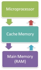
Cache memory is a high-speed memory, which is small in size but faster than the main memory (RAM). The CPU can access it more quickly than the primary memory. So, it is used to synchronize with high-speed CPU and to improve its performance.
|
Fig 2 - Memory
Cache memory can only be accessed by CPU. It can be a reserved part of the main memory or a storage device outside the CPU. It holds the data and programs which are frequently used by the CPU. So, it makes sure that the data is instantly available for CPU whenever the CPU needs this data. In other words, if the CPU finds the required data or instructions in the cache memory, it doesn't need to access the primary memory (RAM). Thus, by acting as a buffer between RAM and CPU, it speeds up the system performance.
L1: It is the first level of cache memory, which is called Level 1 cache or L1 cache. In this type of cache memory, a small amount of memory is present inside the CPU itself. If a CPU has four cores (quad core cpu), then each core will have its own level 1 cache. As this memory is present in the CPU, it can work at the same speed as of the CPU. The size of this memory ranges from 2KB to 64 KB. The L1 cache further has two types of caches: Instruction cache, which stores instructions required by the CPU, and the data cache that stores the data required by the CPU.
L2: This cache is known as Level 2 cache or L2 cache. This level 2 cache may be inside the CPU or outside the CPU. All the cores of a CPU can have their own separate level 2 cache, or they can share one L2 cache among themselves. In case it is outside the CPU, it is connected with the CPU with a very high-speed bus. The memory size of this cache is in the range of 256 KB to the 512 KB. In terms of speed, they are slower than the L1 cache.
L3: It is known as Level 3 cache or L3 cache. This cache is not present in all the processors; some high-end processors may have this type of cache. This cache is used to enhance the performance of Level 1 and Level 2 cache. It is located outside the CPU and is shared by all the cores of a CPU. Its memory size ranges from 1 MB to 8 MB. Although it is slower than L1 and L2 cache, it is faster than Random Access Memory (RAM).
How does cache memory work with CPU?
When CPU needs the data, first of all, it looks inside the L1 cache. If it does not find anything in L1, it looks inside the L2 cache. If again, it does not find the data in L2 cache, it looks into the L3 cache. If data is found in the cache memory, then it is known as a cache hit. On the contrary, if data is not found inside the cache, it is called a cache miss.
If data is not available in any of the cache memories, it looks inside the Random Access Memory (RAM). If RAM also does not have the data, then it will get that data from the Hard Disk Drive.
So, when a computer is started for the first time, or an application is opened for the first time, data is not available in cache memory or in RAM. In this case, the CPU gets the data directly from the hard disk drive. Thereafter, when you start your computer or open an application, CPU can get that data from cache memory or RAM.
Primary Memory is of two types: RAM and ROM.
It is a volatile memory. It means it does not store data or instructions permanently. When you switch on the computer the data and instructions from the hard disk are stored in RAM.
CPU utilizes this data to perform the required tasks. As soon as you shut down the computer the RAM loses all the data.
It is a non-volatile memory. It means it does not lose its data or programs that are written on it at the time of manufacture. So it is a permanent memory that contains all important data and instructions needed to perform important tasks like the boot process.
The secondary storage devices which are built into the computer or connected to the computer are known as a secondary memory of the computer. It is also known as external memory or auxiliary storage.
The secondary memory is accessed indirectly via input/output operations. It is non-volatile, so permanently stores the data even when the computer is turned off or until this data is overwritten or deleted. The CPU can't directly access the secondary memory. First, the secondary memory data is transferred to primary memory then the CPU can access it.
Some of the secondary memory or storage devices are described below:
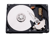
It is a rigid magnetic disc that is used to store data. It permanently stores data and is located within a drive unit.
|
Fig 3 – Hard disk
The hard disk is also known as a hard drive. It is a rigid magnetic disc that stores data permanently, as it is a non-volatile storage device. The hard disk is located within a drive unit on the computer's motherboard and comprises one or more platters packed in an air-sealed casing. The data is written on the platters by moving a magnetic head over the platters as they spin. The data stored on a computer's hard drive generally includes the operating system, installed software, and the user's files and programs, including pictures, music, videos, text documents, etc.
The main components of a hard drive include a head actuator, read/write actuator arm, read/write head, platter, and spindle. A circuit board, which is called the disk controller or interface board, is present on the back of a hard drive. It allows the hard drive to communicate with the computer.
|
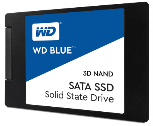
Fig 4 - SSD
SSD (Solid State Drive) is also a non-volatile storage medium that is used to hold and access data. Unlike a hard drive, it does not have moving components, so it offers many advantages over SSD, such as faster access time, noiseless operation, less power consumption, and more.
As the cost of SSD has come down, it has become an ideal replacement for a standard hard drive in desktop and laptop computers. It is also suitable for notebooks, and tablets that don't require lots of storage.
|
Fig 5 – Pen drive
Pen drive is a compact secondary storage device. It is also known as a USB flash drive, thumb drive or a jump drive. It connects to a computer via a USB port. It is commonly used to store and transfer data between computers. For example, you can write a report using a computer and then copy or transfer it in the pen drive. Later, you can connect this pen drive to a computer to see or edit your report. You can also store your important documents and pictures, music, videos in the pen drive and keep it at a safe place.
Pen drive does not have movable parts; it comprises an integrated circuit memory chip that stores the data. This chip is housed inside a plastic or aluminium casing. The data storage capacity of the pen drive generally ranges from 2 GB to 128 GB. Furthermore, it is a plug and play device as you don't need additional drives, software, or hardware to use it.
|
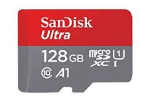
Fig 6 – SD card
SD Card stands for Secure Digital Card. It is most often used in portable and mobile devices such as smartphones and digital cameras. You can remove it from your device and see the things stored in it using a computer with a card reader.
There are many memory chips inside the SD card that store the data; it does not have moving parts. SD cards are not created equal, so they may differ from each other in terms of speed, physical sizes, and capacity. For example, standard SD cards, mini-SD cards, and micro-SD cards.
|
Fig 7 - CD
Compact Disk is a portable secondary storage device in the shape of a round medium disk. It is made of polycarbonate plastic. The concept of CD was co-developed by Philips and Sony in 1982. The first CD was created on 17 August 1982 at the workshop of Philips in Germany.
In the beginning, it was used for storing and playing sound recordings, later it was used for various purposes such as for storing documents, audio files, videos, and other data like software programs in a CD.
Physical characteristics of a CD/ Structure of CD:
A standard CD is around 5 inches in diameter and 0.05 inches in thickness. It is made of a clear polycarbonate plastic substrate, a reflective metallic layer, and a clear coating of acrylic plastic. These thin circular layers are attached one on top of another as described below:
- A polycarbonate disc layer at the bottom has the data encoded by creating lands and pits.
- The polycarbonate disc layer is coated with a thin aluminum layer that reflects the laser.
- The reflective aluminum layer is coated with a lacquer layer to prevent oxidation in order to protect the below layers. It is generally spin coated directly on the top of the reflective layer.
- The label print is applied on the lacquer layer, or artwork is screen printed on the top of the disc on the lacquer layer by offset printing or screen printing.
The data or information is stored or recorded or encoded in CD digitally using a laser beam that etches tiny indentations or bumps on its surface. The bump is called a pit, which represents the number 0. Space, where the bump is not created, is called land, and it represents the number 1. Thus, the data is encoded into a compact disc by creating pits (0) and lands (1). The CD players use laser technology to read the optically recorded data.
|
Fig 8 - DVD
DVD is short for digital versatile disc or digital video disc. It is a type of optical media used for storing optical data. Although it has the same size as a CD, its storage capacity is much more than a CD. So, it is widely used for storing and viewing movies and to distribute software programs as they are too large to fit on a CD. DVD was co-developed by Sony, Panasonic, Philips, and Toshiba in 1995.
DVDs can be divided into three main categories which are as follows:
- DVD-ROM (Read-Only): These types of DVDs come with media already recorded on them, such as movie dvds. As the name suggests, data on these discs cannot be erased or added, so these discs are known as a read-only or non-writable DVD.
- DVD-R (Writable): It allows you to record or write information to the DVD. However, you can write information only once as it becomes a read-only DVD once it is full.
- DVD-RW (Rewritable or Erasable): This type of discs can be erased, written, or recorded multiple times.
I/O devices are very important in the computer systems.They provide users the means of interacting with the system. So there is a separate I/O system devoted to handling the I/O devices.
The different Components of the I/O systems are –
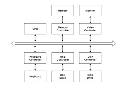
There are many I/O devices handled by the operating system such as mouse, keyboard, disk drive etc. There are different device drivers that can be connected to the operating system to handle a specific device. The device controller is an interface between the device and the device driver.
A diagram to represent this is −
|
Fig 9 – I/O Hardware
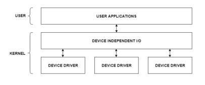
The user applications can access all the I/O devices using the device drivers, which are device specific codes. The application layer sees a common interface for all the devices.
This is illustrated using the below image −
|
Fig 10 – I/O Application Interface
Most of the devices are either block I/O and character I/O devices. Block devices are accessed one block at a time whereas character devices are accessed one character at a time.
The I/O software contains the user level libraries and the kernel modules. The libraries provide the interface to the user program to perform input and output. The kernel modules provide the device drivers that interact with the device controllers.
The I/O software should be device independent so that the programs can be used for any I/O device without specifying it in advance. For example - A program that reads a file should be able the read the file on a hard disk, floppy disk, CD-ROM etc. without having to change the program each time.
During the execution of a program, the control unit fetches one instruction at a time from the main memory and then executes it. In this execution process, it takes help of ALU, if the instruction execution involves arithmetic or logical operation (like AND, OR, Ex-OR). After execution of the current instruction, the CPU fetches the next instruction for execution. This process continues until the program is completed and the result is output using the output device. In many computers, the control unit and the ALU are integrated into a single block, known as Central Processing Unit (CPU).
Central Processing Unit (CPU) consists of the following features −
- CPU is considered as the brain of the computer.
- CPU performs all types of data processing operations.
- It stores data, intermediate results, and instructions (program).
- It controls the operation of all parts of the computer.
|
Fig 11 - Processor
CPU itself has the following three components.
- Memory or Storage Unit
- a control unit
- ALU(Arithmetic Logic Unit)
|
Fig 12 – Control Unit
This unit can store instructions, data, and intermediate results. This unit supplies information to other units of the computer when needed. It is also known as an internal storage unit or the main memory or the primary storage or Random-Access Memory (RAM).
Its size affects speed, power, and capability. Primary memory and secondary memory are two types of memories in the computer. Functions of the memory unit are −
- It stores all the data and the instructions required for processing.
- It stores intermediate results of processing.
- It stores the final results of processing before these results are released to an output device.
- All inputs and outputs are transmitted through the main memory.
This unit controls the operations of all parts of the computer but does not carry out any actual data processing operations.
Functions of this unit are −
- It is responsible for controlling the transfer of data and instructions among other units of a computer.
- It manages and coordinates all the units of the computer.
- It obtains the instructions from the memory, interprets them, and directs the operation of the computer.
- It communicates with Input/output devices for transfer of data or results from storage.
- It does not process or store data.
This unit consists of two subsections namely,
- Arithmetic section
- Logic Section
Arithmetic section
The function of arithmetic section is to perform arithmetic operations like addition, subtraction, multiplication, and division. All complex operations are done by making repetitive use of the above operations.
Logic Section
The function of the logic section is to perform logic operations such as comparing, selecting, matching, and merging of data.
Key takeaway
A Central Processing Unit is also called a processor, central processor, or microprocessor. It carries out all the important functions of a computer. It receives instructions from both the hardware and active software and produces output accordingly. It stores all important programs like operating systems and application software. CPU also helps Input and output devices to communicate with each other. Owing to these features of CPU, it is often referred to as the brain of the computer.
This basically means that an ISA describes the design of a Computer in terms of the basic operations it must support. The ISA is not concerned with the implementation specific details of a computer. It is only concerned with the set or collection of basic operations the computer must support. For example the AMD Athlon and the Core 2 Duo processors have entirely different implementations but they support more or less the same set of basic operations as defined in the x86 Instruction Set.
Let us try to understand the Objectives of an ISA by taking the example of the MIPS ISA. MIPS is one of the most widely used ISAs in education due to its simplicity.
- The ISA defines the types of instructions to be supported by the processor.
Based on the type of operations they perform MIPS Instructions are classified into 3 types:- Arithmetic/Logic Instructions:
These Instructions perform various Arithmetic & Logical operations on one or more operands. - Data Transfer Instructions:
These instructions are responsible for the transfer of instructions from memory to the processor registers and vice versa. - Branch and Jump Instructions:
These instructions are responsible for breaking the sequential flow of instructions and jumping to instructions at various other locations, this is necessary for the implementation of functions and conditional statements.
- Arithmetic/Logic Instructions:
- The ISA defines the maximum length of each type of instruction.
Since the MIPS is a 32 bit ISA, each instruction must be accomodated within 32 bits.
3. The ISA defines the Instruction Format of each type of instruction.
The Instruction Format determines how the entire instruction is encoded within 32 bits
There are 3 types of Instruction Formats in the MIPS ISA:
- R-Instruction Format
- I-Instruction Format
- J-Instruction Format
Each of the above Instruction Formats have different instruction encoding schemes, and hence need to be interpreted differently by the processor.
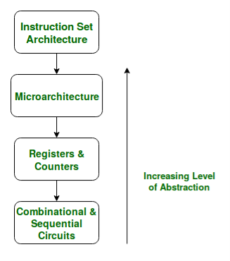
If we look at the Abstraction Hierarchy:
|
Fig 13 – The Abstraction Hierarchy
We note that the Micro architectural level lies just below the ISA level and hence is concerned with the implementation of the basic operations to be supported by the Computer as defined by the ISA. Therefore we can say that the AMD Athlon and Core 2 Duo processors are based on the same ISA but have different microarchitectures with different performance and efficiencies.
Now one may ask the need to distinguish between Microarchitecture and ISA ?
The answer to this lies in the need to standardize and maintain the compatibility of programs across different hardware implementations based on the same ISA. Making different machines compatible with the same set of basic instructions (The ISA) allows the same program to run smoothly on many different machines thereby making it easier for the programmers to document and maintain code for many different machines simultaneously and efficiently.
This Flexibility is the reason we first define an ISA and then design different microarchitectures complying to this ISA for implementing the machine. The design of a ISA is one of the major tasks in the study of Computer Architecture.
Instruction Set Architecture | Microarchitecture |
The ISA is responsible for defining the set of instructions to be supported by the processor. For example, some of the instructions defined by the ARMv7 ISA are given below | The Microarchitecture is more concerned with the lower level implementation of how the instructions are going to be executed and deals with concepts like Instruction Pipelining, Branch Prediction, Out of Order Execution. |
The Branch of Computer Architecture is more inclined towards the Analysis and Design of Instruction Set Architecture.For Example, Intel developed the x86 architecture, ARM developed the ARM architecture, & AMD developed the amd64 architecture. The RISC-V ISA developed by UC Berkeley is an example of a Open Source ISA. | On the other hand the Branch of Computer Organization is concerned with the implementation of a particular ISA deals with various hardware implementation techniques, i.e. is the Microarchitecture level. For Example, ARM licenses other companies like Qualcomm, Apple for using it ARM ISA, but each of these companies have their own implementations of this ISA thereby making them different in performance and power efficiency. The Krait cores developed by Qualcomm have a different microarchitecture and the Apple A-series processors have a different microarchitecture. |
The x86 was developed by Intel, but we see that almost every year Intel comes up with a new generation of i-series processors. The x86 architecture on which most of the Intel Processors are based essentially remains the same across all these generations but, where they differ is in the underlying Microarchitecture. They differ in their implementation, and hence are claimed to have improved Performance. These various Microarchitectures developed by Intel are codenamed as ‘Nehalem’, ‘Sandy bridge’, ‘Ivybridge’ and so on.
Therefore, in conclusion, we can say that different machines may be based on the same ISA, but have different Microarchitectures.
Key takeaway
This basically means that an ISA describes the design of a Computer in terms of the basic operations it must support. The ISA is not concerned with the implementation specific details of a computer. It is only concerned with the set or collection of basic operations the computer must support. For example the AMD Athlon and the Core 2 Duo processors have entirely different implementations but they support more or less the same set of basic operations as defined in the x86 Instruction Set.
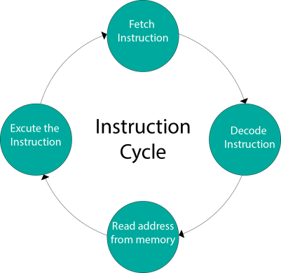
A program residing in the memory unit of a computer consists of a sequence of instructions. These instructions are executed by the processor by going through a cycle for each instruction.
In a basic computer, each instruction cycle consists of the following phases:
- Fetch instruction from memory.
- Decode the instruction.
- Read the effective address from memory.
- Execute the instruction.
|
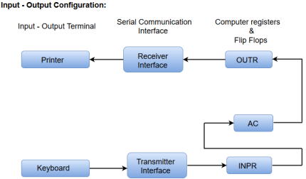
Fig 14 - Input-Output Configuration
In computer architecture, input-output devices act as an interface between the machine and the user.
Instructions and data stored in the memory must come from some input device. The results are displayed to the user through some output device.
The following block diagram shows the input-output configuration for a basic computer.
|
Fig 15 – I/O configuration
- The input-output terminals send and receive information.
- The amount of information transferred will always have eight bits of an alphanumeric code.
- The information generated through the keyboard is shifted into an input register 'INPR'.
- The information for the printer is stored in the output register 'OUTR'.
- Registers INPR and OUTR communicate with a communication interface serially and with the AC in parallel.
- The transmitter interface receives information from the keyboard and transmits it to INPR.
- The receiver interface receives information from OUTR and sends it to the printer serially.
A basic computer consists of the following hardware components.
- A memory unit with 4096 words of 16 bits each
- Registers: AC (Accumulator), DR (Data register), AR (Address register), IR (Instruction register), PC (Program counter), TR (Temporary register), SC (Sequence Counter), INPR (Input register), and OUTR (Output register).
- Flip-Flops: I, S, E, R, IEN, FGI and FGO
Note: FGI and FGO are corresponding input and output flags which are considered as control flip-flops.
- Two decoders: a 3 x 8 operation decoder and 4 x 16 timing decoder
- A 16-bit common bus
- Control Logic Gates
- The Logic and Adder circuits connected to the input of AC.
Key takeaway
A program residing in the memory unit of a computer consists of a sequence of instructions. These instructions are executed by the processor by going through a cycle for each instruction.
In a basic computer, each instruction cycle consists of the following phases:
- Fetch instruction from memory.
- Decode the instruction.
- Read the effective address from memory.
- Execute the instruction.
A digital computer system exhibits an interconnection of digital modules such as registers, decoders, arithmetic elements, and Control logic.
These digital modules are interconnected with some common data and control paths to form a complete digital system.
Moreover, digital modules are best defined by the registers and the operations that are performed on the data stored in them.
The operations performed on the data stored in registers are called Micro-operations.
The internal hardware organization of a digital system is best defined by specifying:
- The set of registers and the flow of data between them.
- The sequence of micro-operations performed on the data which are stored in the registers.
- The control paths that initiate the sequence of micro-operation
The Register Transfer Language is the symbolic representation of notations used to specify the sequence of micro-operations.
In a computer system, data transfer takes place between processor registers and memory and between processor registers and input-output systems. These data transfer can be represented by standard notations given below:
- Notations R0, R1, R2..., and so on represent processor registers.
- The addresses of memory locations are represented by names such as LOC, PLACE, MEM, etc.
- Input-output registers are represented by names such as DATA IN, DATA OUT and so on.
- The content of register or memory location is denoted by placing square brackets around the name of the register or memory location.
Key takeaway
A digital computer system exhibits an interconnection of digital modules such as registers, decoders, arithmetic elements, and Control logic.
These digital modules are interconnected with some common data and control paths to form a complete digital system.
Moreover, digital modules are best defined by the registers and the operations that are performed on the data stored in them.
The operations performed on the data stored in registers are called Micro-operations.
Addressing Modes– The term addressing modes refers to the way in which the operand of an instruction is specified. The addressing mode specifies a rule for interpreting or modifying the address field of the instruction before the operand is actually executed.
Addressing modes for 8086 instructions are divided into two categories:
1) Addressing modes for data
2) Addressing modes for branch
The 8086 memory addressing modes provide flexible access to memory, allowing you to easily access variables, arrays, records, pointers, and other complex data types. The key to good assembly language programming is the proper use of memory addressing modes.
An assembly language program instruction consists of two parts
|
Fig 16 - Assembly language program instruction
The memory address of an operand consists of two components:
IMPORTANT TERMS
- Starting address of memory segment.
- Effective address or Offset: An offset is determined by adding any combination of three address elements: displacement, base and index.
- Displacement: It is an 8 bit or 16 bit immediate value given in the instruction.
- Base: Contents of base register, BX or BP.
- Index: Content of index register SI or DI.
According to different ways of specifying an operand by 8086 microprocessor, different addressing modes are used by 8086.
Addressing modes used by 8086 microprocessors are discussed below:
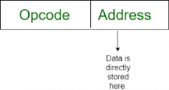
- Implied mode: In implied addressing the operand is specified in the instruction itself. In this mode the data is 8 bits or 16 bits long and data is the part of instruction. Zero address instruction are designed with implied addressing mode.
|
Example: CLC (used to reset Carry flag to 0)
- Immediate addressing mode (symbol #):In this mode data is present in address field of instruction .Designed like one address instruction format.
Note: Limitation in the immediate mode is that the range of constants are restricted by size of address field.
|
Example: MOV AL, 35H (move the data 35H into AL register)
- Register mode: In register addressing the operand is placed in one of 8 bit or 16-bit general purpose registers. The data is in the register that is specified by the instruction.
Here one register reference is required to access the data.
|
Example: MOV AX,CX (move the contents of CX register to AX register)
- Register Indirect mode: In this addressing the operand’s offset is placed in any one of the registers BX,BP,SI,DI as specified in the instruction. The effective address of the data is in the base register or an index register that is specified by the instruction.
Here two register reference is required to access the data.
|
Fig 17 – Register Indirect mode
The 8086 CPUs let you access memory indirectly through a register using the register indirect addressing modes.
- MOV AX, [BX](move the contents of memory location s
addressed by the register BX to the register AX)
- Auto Indexed (increment mode): Effective address of the operand is the contents of a register specified in the instruction. After accessing the operand, the contents of this register are automatically incremented to point to the next consecutive memory location.(R1)+.
Here one register reference, one memory reference and one ALU operation is required to access the data.
Example:
- Add R1, (R2)+ // OR
- R1 = R1 +M[R2]
R2 = R2 + d
Useful for stepping through arrays in a loop. R2 – start of array d – size of an element
- Auto indexed (decrement mode): Effective address of the operand is the contents of a register specified in the instruction. Before accessing the operand, the contents of this register are automatically decremented to point to the previous consecutive memory location. –(R1)
Here one register reference, one memory reference and one ALU operation is required to access the data.
Example:
Add R1,-(R2) //OR
R2 = R2-d
R1 = R1 + M[R2]
Auto decrement mode is same as auto increment mode. Both can also be used to implement a stack as push and pop . Auto increment and Auto decrement modes are useful for implementing “Last-In-First-Out” data structures.
- Direct addressing/ Absolute addressing Mode (symbol [ ]): The operand’s offset is given in the instruction as an 8 bit or 16 bit displacement element. In this addressing mode the 16-bit effective address of the data is the part of the instruction.
Here only one memory reference operation is required to access the data.
|
Fig 18 - Example
Example: ADD AL, [0301] //add the contents of offset address 0301 to AL
- Indirect addressing Mode (symbol @ or ()): In this mode address field of instruction contains the address of effective address. Here two references are required.
1st reference to get effective address.
2nd reference to access the data.
Based on the availability of Effective address, Indirect mode is of two kind:
- Register Indirect: In this mode effective address is in the register, and corresponding register name will be maintained in the address field of an instruction.
Here one register reference, one memory reference is required to access the data. - Memory Indirect: In this mode effective address is in the memory, and corresponding memory address will be maintained in the address field of an instruction.
Here two memory reference is required to access the data.
- Indexed addressing mode: The operand’s offset is the sum of the content of an index register SI or DI and an 8 bit or 16-bit displacement.
Example AX, [SI +05]
- Based Indexed Addressing: The operand’s offset is sum of the content of a base register BX or BP and an index register SI or DI.
Example: ADD AX, [BX+SI]
Based on Transfer of control, addressing modes are:
- PC relative addressing mode: PC relative addressing mode is used to implement intra segment transfer of control, In this mode effective address is obtained by adding displacement to PC.
- EA= PC + Address field value
PC= PC + Relative value.
3. Base register addressing mode: Base register addressing mode is used to implement inter segment transfer of control. In this mode effective address is obtained by adding base register value to address field value.
4. EA= Base register + Address field value.
5. PC= Base register + Relative value.
Note:
PC relative nad based register both addressing modes are suitable for program relocation at runtime.
Based register addressing mode is best suitable to write position independent codes.
Advantages of Addressing Modes
To give programmers to facilities such as Pointers, counters for loop controls, indexing of data and program relocation.
To reduce the number bits in the addressing field of the Instruction.
Key takeaway
Addressing Modes– The term addressing modes refers to the way in which the operand of an instruction is specified. The addressing mode specifies a rule for interpreting or modifying the address field of the instruction before the operand is actually executed.
Computer instructions are a set of machine language instructions that a particular processor understands and executes. A computer performs tasks on the basis of the instruction provided.
An instruction comprises of groups called fields. These fields include:
- The Operation code (Opcode) field which specifies the operation to be performed.
- The Address field which contains the location of the operand, i.e., register or memory location.
- The Mode field which specifies how the operand will be located.
|
Fig 19 – Mode field
A basic computer has three instruction code formats which are:
- Memory - reference instruction
- Register - reference instruction
- Input-Output instruction
Fig 20 - Memory - reference instruction
|
In Memory-reference instruction, 12 bits of memory is used to specify an address and one bit to specify the addressing mode 'I'.
Fig 21 - Register - reference instruction
|
The Register-reference instructions are represented by the Opcode 111 with a 0 in the leftmost bit (bit 15) of the instruction.
Note: The Operation code (Opcode) of an instruction refers to a group of bits that define arithmetic and logic operations such as add, subtract, multiply, shift, and compliment.
A Register-reference instruction specifies an operation on or a test of the AC (Accumulator) register.
Fig 22 - Input-Output instruction
|
Just like the Register-reference instruction, an Input-Output instruction does not need a reference to memory and is recognized by the operation code 111 with a 1 in the leftmost bit of the instruction. The remaining 12 bits are used to specify the type of the input-output operation or test performed.
- The three operation code bits in positions 12 through 14 should be equal to 111. Otherwise, the instruction is a memory-reference type, and the bit in position 15 is taken as the addressing mode I.
- When the three operation code bits are equal to 111, control unit inspects the bit in position 15. If the bit is 0, the instruction is a register-reference type. Otherwise, the instruction is an input-output type having bit 1 at position 15.
A set of instructions is said to be complete if the computer includes a sufficient number of instructions in each of the following categories:
- Arithmetic, logical and shift instructions
- A set of instructions for moving information to and from memory and processor registers.
- Instructions which controls the program together with instructions that check status conditions.
- Input and Output instructions
Arithmetic, logic and shift instructions provide computational capabilities for processing the type of data the user may wish to employ.
A huge amount of binary information is stored in the memory unit, but all computations are done in processor registers. Therefore, one must possess the capability of moving information between these two units.
Program control instructions such as branch instructions are used change the sequence in which the program is executed.
Input and Output instructions act as an interface between the computer and the user. Programs and data must be transferred into memory, and the results of computations must be transferred back to the user.
Key takeaway
Computer instructions are a set of machine language instructions that a particular processor understands and executes. A computer performs tasks on the basis of the instruction provided.
An instruction comprises of groups called fields. These fields include:
- The Operation code (Opcode) field which specifies the operation to be performed.
- The Address field which contains the location of the operand, i.e., register or memory location.
- The Mode field which specifies how the operand will be located.
The Instruction Set Architecture (ISA) is the part of the processor that is visible to the programmer or compiler writer. The ISA serves as the boundary between software and hardware. We will briefly describe the instruction sets found in many of the microprocessors used today. The ISA of a processor can be described using 5 categories:
Operand Storage in the CPU
Where are the operands kept other than in memory?
Number of explicit named operands
How many operands are named in a typical instruction?
Operand location
Can any ALU instruction operand be located in memory? Or must all operands be kept internally in the CPU?
Operations
What operations are provided in the ISA.
Type and size of operands
What is the type and size of each operand and how is it specified?
Of all the above the most distinguishing factor is the first.
The 3 most common types of ISAs are:
- Stack - The operands are implicitly on top of the stack.
- Accumulator - One operand is implicitly the accumulator.
- General Purpose Register (GPR) - All operands are explicitely mentioned, they are either registers or memory locations.
Lets look at the assembly code of
C = A + B;
in all 3 architectures:
Stack | Accumulator | GPR |
PUSH A | LOAD A | LOAD R1,A |
PUSH B | ADD B | ADD R1,B |
ADD | STORE C | STORE R1,C |
POP C | - | - |
Not all processors can be neatly tagged into one of the above catagories. The i8086 has many instructions that use implicit operands although it has a general register set. The i8051 is another example, it has 4 banks of GPRs but most instructions must have the A register as one of its operands.
What are the advantages and disadvantages of each of these approachs?
Advantages: Simple Model of expression evaluation (reverse polish). Short instructions.
Disadvantages: A stack can't be randomly accessed This makes it hard to generate efficient code. The stack itself is accessed every operation and becomes a bottleneck.
Advantages: Short instructions.
Disadvantages: The accumulator is only temporary storage so memory traffic is the highest for this approach.
Advantages: Makes code generation easy. Data can be stored for long periods in registers.
Disadvantages: All operands must be named leading to longer instructions.
Earlier CPUs were of the first 2 types but in the last 15 years all CPUs made are GPR processors. The 2 major reasons are that registers are faster than memory, the more data that can be kept internally in the CPU the faster the program will run. The other reason is that registers are easier for a compiler to use.
Reduced Instruction Set Computer (RISC)
As we mentioned before most modern CPUs are of the GPR (General Purpose Register) type. A few examples of such CPUs are the IBM 360, DEC VAX, Intel 80x86 and Motorola 68xxx. But while these CPUS were clearly better than previous stack and accumulator-based CPUs they were still lacking in several areas:
- Instructions were of varying length from 1 byte to 6-8 bytes. This causes problems with the pre-fetching and pipelining of instructions.
- ALU (Arithmetic Logical Unit) instructions could have operands that were memory locations. Because the number of cycles it takes to access memory varies so does the whole instruction. This isn't good for compiler writers, pipelining and multiple issue.
- Most ALU instructions had only 2 operands where one of the operands is also the destination. This means this operand is destroyed during the operation or it must be saved before somewhere.
Thus in the early 80's the idea of RISC was introduced. The SPARC project was started at Berkeley and the MIPS project at Stanford. RISC stands for Reduced Instruction Set Computer. The ISA is composed of instructions that all have exactly the same size, usually 32 bits. Thus, they can be pre-fetched and pipelined successfully. All ALU instructions have 3 operands which are only registers. The only memory access is through explicit LOAD/STORE instructions.
Thus C = A + B will be assembled as:
LOAD R1,A
LOAD R2,B
ADD R3,R1,R2
STORE C,R3
Although it takes 4 instructions, we can reuse the values in the registers.
Why is this architecture called RISC? What is Reduced about it?
The answer is that to make all instructions the same length the number of bits that are used for the opcode is reduced. Thus, less instructions are provided. The instructions that were thrown out are the less important string and BCD (binary-coded decimal) operations. In fact, now that memory access is restricted there aren't several kinds of MOV or ADD instructions. Thus, the older architecture is called CISC (Complete Instruction Set Computer). RISC architectures are also called LOAD/STORE architectures.
The number of registers in RISC is usually 32 or more. The first RISC CPU the MIPS 2000 has 32 GPRs as opposed to 16 in the 68xxx architecture and 8 in the 80x86 architecture. The only disadvantage of RISC is its code size. Usually more instructions are needed and there is a waste in short instructions (POP, PUSH).
So why are there still CISC CPUs being developed? Why is Intel spending time and money to manufacture the Pentium II and the Pentium III?
The answer is simple, backward compatibility. The IBM compatible PC is the most common computer in the world. Intel wanted a CPU that would run all the applications that are in the hands of more than 100 million users. On the other hand, Motorola which builds the 68xxx series which was used in the Macintosh made the transition and together with IBM and Apple built the Power PC (PPC) a RISC CPU which is installed in the new Power Macs. As of now Intel and the PC manufacturers are making more money but with Microsoft playing in the RISC field as well (Windows NT runs on Compaq's Alpha) and with the promise of Java the future of CISC isn't clear at all.
Key takeaway
The Instruction Set Architecture (ISA) is the part of the processor that is visible to the programmer or compiler writer. The ISA serves as the boundary between software and hardware. We will briefly describe the instruction sets found in many of the microprocessors used today.
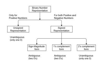
Variables such as integers can be representing in two ways, i.e., signed and unsigned. Signed numbers use sign flag or can be distinguish between negative values and positive values. Whereas unsigned numbers stored only positive numbers but not negative numbers.
Number representation techniques like: Binary, Octal, Decimal and Hexadecimal number representation techniques can represent numbers in both signed and unsigned ways. Binary Number System is one the type of Number Representation techniques. It is most popular and used in digital systems. Binary system is used for representing binary quantities which can be represented by any device that has only two operating states or possible conditions. For example, a switch has only two states: open or close.
In the Binary System, there are only two symbols or possible digit values, i.e., 0 and 1. Represented by any device that only 2 operating states or possible conditions. Binary numbers are indicated by the addition of either an 0b prefix or a 2 suffix.
Representation of Binary Numbers:
Binary numbers can be represented in signed and unsigned way. Unsigned binary numbers do not have sign bit, whereas signed binary numbers uses signed bit as well or these can be distinguishable between positive and negative numbers. A signed binary is a specific data type of a signed variable.
|
Fig 23 – Binary number representation
1. Unsigned Numbers:
Unsigned numbers don’t have any sign, these can contain only magnitude of the number. So, representation of unsigned binary numbers are all positive numbers only. For example, representation of positive decimal numbers are positive by default. We always assume that there is a positive sign symbol in front of every number.
Representation of Unsigned Binary Numbers:
Since there is no sign bit in this unsigned binary number, so N bit binary number represent its magnitude only. Zero (0) is also unsigned number. This representation has only one zero (0), which is always positive. Every number in unsigned number representation has only one unique binary equivalent form, so this is unambiguous representation technique. The range of unsigned binary number is from 0 to (2n-1).
Example-1: Represent decimal number 92 in unsigned binary number.
Simply convert it into Binary number, it contains only magnitude of the given number.
= (92)10
= (1x26+0x25+1x24+1x23+1x22+0x21+0x20)10
= (1011100)2
It’s 7-bit binary magnitude of the decimal number 92.
Example-2: Find range of 5-bit unsigned binary numbers. Also, find minimum and maximum value in this range.
Since, range of unsigned binary number is from 0 to (2n-1). Therefore, range of 5-bit unsigned binary number is from 0 to (25-1) which is equal from minimum value 0 (i.e., 00000) to maximum value 31 (i.e., 11111).
2. Signed Numbers:
Signed numbers contain sign flag, this representation distinguishes positive and negative numbers. This technique contains both sign bit and magnitude of a number. For example, in representation of negative decimal numbers, we need to put negative symbol in front of given decimal number.
Representation of Signed Binary Numbers:
There are three types of representations for signed binary numbers. Because of extra signed bit, binary number zero has two representation, either positive (0) or negative (1), so ambiguous representation. But 2’s complementation representation is unambiguous representation because of there is no double representation of number 0. These are: Sign-Magnitude form, 1’s complement form, and 2’s complement form which are explained as following below.
2.(a) Sign-Magnitude form:
For n bit binary number, 1 bit is reserved for sign symbol. If the value of sign bit is 0, then the given number will be positive, else if the value of sign bit is 1, then the given number will be negative. Remaining (n-1) bits represent magnitude of the number. Since magnitude of number zero (0) is always 0, so there can be two representation of number zero (0), positive (+0) and negative (-0), which depends on value of sign bit. Hence these representations are ambiguous generally because of two representation of number zero (0). Generally, sign bit is a most significant bit (MSB) of representation. The range of Sign-Magnitude form is from (2(n-1)-1) to (2(n-1)-1).
For example, range of 6-bit Sign-Magnitude form binary number is from (25-1) to (25-1) which is equal from minimum value -31 (i.e., 1 11111) to maximum value +31 (i.e., 0 11111). And zero (0) has two representation, -0 (i.e., 1 00000) and +0 (i.e., 0 00000).
2.(b) 1’s complement form:
Since, 1’s complement of a number is obtained by inverting each bit of given number. So, we represent positive numbers in binary form and negative numbers in 1’s complement form. There is extra bit for sign representation. If value of sign bit is 0, then number is positive and you can directly represent it in simple binary form, but if value of sign bit 1, then number is negative and you have to take 1’s complement of given binary number. You can get negative number by 1’s complement of a positive number and positive number by using 1’s complement of a negative number. Therefore, in this representation, zero (0) can have two representation, that’s why 1’s complement form is also ambiguous form. The range of 1’s complement form is from (2(n-1)-1) to (2(n-1)-1) .
For example, range of 6 bit 1’s complement form binary number is from (25-1) to (25-1) which is equal from minimum value -31 (i.e., 1 00000) to maximum value +31 (i.e., 0 11111). And zero (0) has two representation, -0 (i.e., 1 11111) and +0 (i.e., 0 00000).
2.(c) 2’s complement form:
Since, 2’s complement of a number is obtained by inverting each bit of given number plus 1 to least significant bit (LSB). So, we represent positive numbers in binary form and negative numbers in 2’s complement form. There is extra bit for sign representation. If value of sign bit is 0, then number is positive and you can directly represent it in simple binary form, but if value of sign bit 1, then number is negative and you have to take 2’s complement of given binary number. You can get negative number by 2’s complement of a positive number and positive number by directly using simple binary representation. If value of most significant bit (MSB) is 1, then take 2’s complement from, else not. Therefore, in this representation, zero (0) has only one (unique) representation which is always positive. The range of 2’s complement form is from (2(n-1)) to (2(n-1)-1).
For example, range of 6 bit 2’s complement form binary number is from (25) to (25-1) which is equal from minimum value -32 (i.e., 1 00000) to maximum value +31 (i.e., 0 11111). And zero (0) has two representation, -0 (i.e., 1 11111) and +0 (i.e., 0 00000).
Key takeaway
Variables such as integers can be representing in two ways, i.e., signed and unsigned. Signed numbers use sign flag or can be distinguish between negative values and positive values. Whereas unsigned numbers stored only positive numbers but not negative numbers.
Number representation techniques like: Binary, Octal, Decimal and Hexadecimal number representation techniques can represent numbers in both signed and unsigned ways. Binary Number System is one the type of Number Representation techniques. It is most popular and used in digital systems. Binary system is used for representing binary quantities which can be represented by any device that has only two operating states or possible conditions. For example, a switch has only two states: open or close.
Digital Computers use Binary number system to represent all types of information inside the computers. Alphanumeric characters are represented using binary bits (i.e., 0 and 1). Digital representations are easier to design, storage is easy, accuracy and precision are greater.
There are various types of number representation techniques for digital number representation, for example: Binary number system, octal number system, decimal number system, and hexadecimal number system etc. But Binary number system is most relevant and popular for representing numbers in digital computer system.
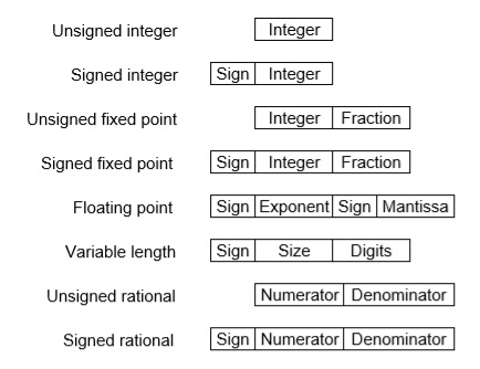
These are structures as following below −
|
There are two major approaches to store real numbers (i.e., numbers with fractional component) in modern computing. These are (i) Fixed Point Notation and (ii) Floating Point Notation. In fixed point notation, there are a fixed number of digits after the decimal point, whereas floating point number allows for a varying number of digits after the decimal point.
Fixed-Point Representation −
This representation has fixed number of bits for integer part and for fractional part. For example, if given fixed-point representation is IIII.FFFF, then you can store minimum value is 0000.0001 and maximum value is 9999.9999. There are three parts of a fixed-point number representation: the sign field, integer field, and fractional field.
|
We can represent these numbers using:
- Signed representation: range from -(2(k-1)-1) to (2(k-1)-1), for k bits.
- 1’s complement representation: range from -(2(k-1)-1) to (2(k-1)-1), for k bits.
- 2’s complementation representation: range from -(2(k-1)) to (2(k-1)-1), for k bits.
2’s complementation representation is preferred in computer system because of unambiguous property and easier for arithmetic operations.
Example −Assume number is using 32-bit format which reserve 1 bit for the sign, 15 bits for the integer part and 16 bits for the fractional part.
Then, -43.625 is represented as following:
|
Where, 0 is used to represent + and 1 is used to represent. 000000000101011 is 15-bit binary value for decimal 43 and 1010000000000000 is 16 bit binary value for fractional 0.625.
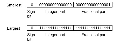
The advantage of using a fixed-point representation is performance and disadvantage is relatively limited range of values that they can represent. So, it is usually inadequate for numerical analysis as it does not allow enough numbers and accuracy. A number whose representation exceeds 32 bits would have to be stored inexactly.
|
These are above smallest positive number and largest positive number which can be store in 32-bit representation as given above format. Therefore, the smallest positive number is 2-16 ≈ 0.000015 approximate and the largest positive number is (215-1) +(1-2-16) =215(1-2-16) =32768, and gap between these numbers is 2-16.
We can move the radix point either left or right with the help of only integer field is 1.
Floating-Point Representation −
This representation does not reserve a specific number of bits for the integer part or the fractional part. Instead, it reserves a certain number of bits for the number (called the mantissa or significand) and a certain number of bits to say where within that number the decimal place sits (called the exponent).
The floating number representation of a number has two part: the first part represents a signed fixed-point number called mantissa. The second part of designates the position of the decimal (or binary) point and is called the exponent. The fixed-point mantissa may be fraction or an integer. Floating -point is always interpreted to represent a number in the following form: Mxre.
Only the mantissa m and the exponent e are physically represented in the register (including their sign). A floating-point binary number is represented in a similar manner except that is uses base 2 for the exponent. A floating-point number is said to be normalized if the most significant digit of the mantissa is 1.
|
So, actual number is (-1)s(1+m)x2(e-Bias), where s is the sign bit, m is the mantissa, e is the exponent value, and Bias is the bias number.
Note that signed integers and exponent are represented by either sign representation, or one’s complement representation, or two’s complement representation.
The floating-point representation is more flexible. Any non-zero number can be represented in the normalized form of ± (1.b1b2b3 ...)2x2n This is normalized form of a number x.
Example −Suppose number is using 32-bit format: the 1-bit sign bit, 8 bits for signed exponent, and 23 bits for the fractional part. The leading bit 1 is not stored (as it is always 1 for a normalized number) and is referred to as a “hidden bit”.
Then −53.5 is normalized as -53.5= (-110101.1)2= (-1.101011) x25, which is represented as following below,
|
Where 00000101 is the 8-bit binary value of exponent value +5.
Note that 8-bit exponent field is used to store integer exponents -126 ≤ n ≤ 127.
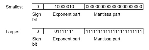
The smallest normalized positive number that fits into 32 bits is (1.00000000000000000000000)2x2-126=2-126≈1.18x10-38, and largest normalized positive number that fits into 32 bits is (1.11111111111111111111111)2x2127= (224-1)x2104 ≈ 3.40x1038 . These numbers are represented as following below,
|
The precision of a floating-point format is the number of positions reserved for binary digits plus one (for the hidden bit). In the examples considered here the precision is 23+1=24.
The gap between 1 and the next normalized floating-point number is known as machine epsilon. the gap is (1+2-23)-1=2-23for above example, but this is same as the smallest positive floating-point number because of non-uniform spacing unlike in the fixed-point scenario.
Note that non-terminating binary numbers can be represented in floating point representation, e.g., 1/3 = (0.010101 ...)2 cannot be a floating-point number as its binary representation is non-terminating.
IEEE Floating point Number Representation −
IEEE (Institute of Electrical and Electronics Engineers) has standardized Floating-Point Representation as following diagram.
|
So, actual number is (-1)s(1+m)x2(e-Bias), where s is the sign bit, m is the mantissa, e is the exponent value, and Bias is the bias number. The sign bit is 0 for positive number and 1 for negative number. Exponents are represented by or two’s complement representation.
According to IEEE 754 standard, the floating-point number is represented in following ways:
- Half Precision (16 bit): 1 sign bit, 5 bits exponent, and 10-bit mantissa
- Single Precision (32 bit): 1 sign bit, 8 bit exponent, and 23-bit mantissa
- Double Precision (64 bit): 1 sign bit, 11 bit exponent, and 52-bit mantissa
- Quadruple Precision (128 bit): 1 sign bit, 15 bit exponent, and 112-bit mantissa
Special Value Representation −
There are some special values depended upon different values of the exponent and mantissa in the IEEE 754 standard.
- All the exponent bits 0 with all mantissa bits 0 represents 0. If sign bit is 0, then +0, else -0.
- All the exponent bits 1 with all mantissa bits 0 represents infinity. If sign bit is 0, then +∞, else -∞.
- All the exponent bits 0 and mantissa bits non-zero represents denormalized number.
- All the exponent bits 1 and mantissa bits non-zero represents error.
Key takeaway
Digital Computers use Binary number system to represent all types of information inside the computers. Alphanumeric characters are represented using binary bits (i.e., 0 and 1). Digital representations are easier to design, storage is easy, accuracy and precision are greater.
There are various types of number representation techniques for digital number representation, for example: Binary number system, octal number system, decimal number system, and hexadecimal number system etc. But Binary number system is most relevant and popular for representing numbers in digital computer system.
Everything represented by a computer is represented by binary sequences.
A common non-integer to be represented is a character. We use standard encodings (binary sequences) to represent characters.
REMEMBER: bit patterns do NOT imply a representation
A 4-bit binary quantity is called a nibble. An 8-bit binary quantity is called a byte.
Many I/O devices work with 8-bit quantities. A standard code ASCII (American Standard for Computer Information Interchange) defines what character is represented by each sequence. You'll look these up in an ASCII table.
Examples:
0100 0001 is 41 (hex) or 65 (decimal). It represents 'A'
0100 0010 is 42 (hex) or 66 (decimal). It represents 'B'
Different bit patterns are used for each different character that needs to be represented.
The code has some nice properties. If the bit patterns are compared, (pretending they represent integers), then 'A' < 'B'. This is good, because it helps with sorting things into alphabetical order.
Notes:
- 'a' (0x61) is different than 'A' (0x41)
- '8' (0x38) is different than the integer 8
two's complement representation for 8: 0000 0000 0000 0000 0000 0000 0000 1000
the ASCII character '8': 0011 1000
- the digits:
'0' is 48 (decimal) or 0x30
'9' is 57 (decimal) or 0x39
Because of this difference between the integer representation for a character, and the character representation for a character, we constantly need to convert from one to the other.
The computer does arithmetic operations on two's complement integers (and often operations on unsigned integers). The computer has the ability to read in or print out a single character representation at a time. So, any time we want to do I/O, we're working with one character at a time, and the ASCII representation of the character. Yet, lots of the time, the data represents numbers (just consider integers, for now).
Characters that represent an integer
To read in an integer, and then process the integer, consider an example. Suppose the user types the 4-character sequence 123\n.
The computer can read in a single character at a time. If it reads in exactly 4 characters, then the representations that the computer will have will be
ASCII decimal binary integer 8-bit two's comp.
character hex value desired representation
'1' 0x31 49 00110001 1 00000001
'2' 0x32 50 00110010 2 00000010
'3' 0x33 51 00110011 3 00000011
'\n' 0x0a 10 00001010 (NA) (NA)
From this example, it should be easy to see that conversion of a single ASCII character representation to the desired two's complement integer representation does an integer subtraction.
integer rep desired = ASCII representation - 48
What we need is an algorithm for translating multi-character strings to the integers they represent, and vice versa.
ALGORITHM: character string --> integer
the steps:
for '3' '5' '4'
integer = 0
read '3'
translate '3' to 3
integer = integer * 10 + 3 = 3
read '5'
translate '5' to 5
integer = integer * 10 + 5 = 35
read '4'
translate '4' to 4
integer = integer * 10 + 4 = 354
the algorithm:
integer = 0
while there are more characters
get character
digit <- character - 48
integer <- integer * 10 + digit
Going the other direction for translation (integer to set of characters represented, printed out in the correct order), we partially reverse the algorithm.
ALGORITHM: integer --> character string
the steps:
For 354, figure out how many characters there are in
the base desired (3).
Figure out base^(number of characters - 1) (10^2)=100
354 div 100 gives 3
translate 3 to '3' and print it out
354 % 100 gives 54
100/10 = 10
54 div 10 gives 5
translate 5 to '5' and print it out
54 mod 10 gives 4
10/10 = 1
4 div 1 gives 4
translate 4 to '4' and print it out
4 mod 1 gives 0
1/10 = 0, so you're done
written in a form using two loops:
# figure out base^(number of characters - 1)
power_of_base = base
while power_of_base is not large enough
power_of_base = power_of_base * base
while power_of_base != 0
digit = integer / power_of_base
char_to_print = digit + 48
print char_to_print
integer = integer % power_of_base # remainder after integer division
power_of_base = power_of_base / base # quotient
Key takeaway
Everything represented by a computer is represented by binary sequences.
A common non-integer to be represented is a character. We use standard encodings (binary sequences) to represent characters.
REMEMBER: bit patterns do NOT imply a representation
A 4-bit binary quantity is called a nibble. An 8-bit binary quantity is called a byte.
Many I/O devices work with 8-bit quantities. A standard code ASCII (American Standard for Computer Information Interchange) defines what character is represented by each sequence. You'll look these up in an ASCII table.
Operations we'll get to know:
addition
subtraction
multiplication
division
logical operations (not, and, or, nand, nor, xor, xnor)
shifting
the rules for doing the arithmetic operations vary depending
on what representation is implied.
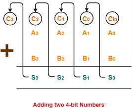
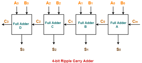
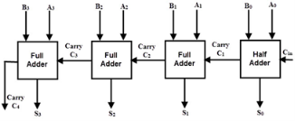
A LITTLE BIT ON ADDING
----------------------
an overview.
carry in a b | sum carry out
---------------+----------------
0 0 0 | 0 0
0 0 1 | 1 0
0 1 0 | 1 0
0 1 1 | 0 1
1 0 0 | 1 0
1 0 1 | 0 1
1 1 0 | 0 1
1 1 1 | 1 1
|
a 0011
+b +0001
-- -----
sum 0100
its really just like we do for decimal!
0 + 0 = 0
1 + 0 = 1
1 + 1 = 2 which is 10 in binary, sum is 0 and carry the 1.
1 + 1 + 1 = 3 sum is 1, and carry a 1.
ADDITION
--------
unsigned:
just like the simple addition given.
examples:
100001 00001010 (10)
+011101 +00001110 (14)
------- ---------
111110 00011000 (24)
ignore (throw away) carry out of the msb.
Why? Because computers ALWAYS work with a fixed precision.
sign magnitude:
rules:
- add magnitudes only (do not carry into the sign bit)
- throw away any carry out of the msb of the magnitude
(Due, again, to the fixed precision constraints.)
- add only integers of like sign ( + to + or - to -)
- sign of result is same as sign of the addends
examples:
0 0101 (5) 1 1010 (-10)
+ 0 0011 (3) + 1 0011 (-3)
--------- ---------
0 1000 (8) 1 1101 (-13)
0 01011 (11)
+ 1 01110 (-14)
----------------
don't add! must do subtraction!
one's complement:
by example
00111 (7) 111110 (-1) 11110 (-1) + 00101 (5) + 000010 (2) + 11100 (-3) ----------- ------------ ------------ 01100 (12) 1 000000 (0) wrong! 1 11010 (-5) wrong! + 1 + 1 ---------- ---------- 000001 (1) right! 11011 (-4) right!
|
so it seems that if there is a carry out (of 1) from the msb, then
the result will be off by 1, so add 1 again to get the correct
result. (Implementation in HW called an "end around carrry.")
two's complement:
rules:
- just add all the bits
- throw away any carry out of the msb
- (same as for unsigned!)
examples
00011 (3) 101000 111111 (-1) + 11100 (-4) + 010000 + 001000 (8) ------------ -------- -------- 11111 (-1) 111000 1 000111 (7)
|
after seeing examples for all these representations, you may see
why 2's complement addition requires simpler hardware than
sign mag. or one's complement addition.
SUBTRACTION
-----------
general rules:
1 - 1 = 0
0 - 0 = 0
1 - 0 = 1
10 - 1 = 1
0 - 1 = borrow!
unsigned:
- it only makes sense to subtract a smaller number from a larger one
examples
1011 (11) must borrow
- 0111 (7)
------------
0100 (4)
sign magnitude:
- if the signs are the same, then do subtraction
- if signs are different, then change the problem to addition
- compare magnitudes, then subtract smaller from larger
- if the order is switched, then switch the sign too.
- when the integers are of the opposite sign, then do
a - b becomes a + (-b)
a + b becomes a - (-b)
examples
0 00111 (7) 1 11000 (-24)
- 0 11000 (24) - 1 00010 (-2)
-------------- --------------
1 10110 (-22)
do 0 11000 (24)
- 0 00111 (7)
--------------
1 10001 (-17)
(switch sign since the order of the subtraction was reversed)
one's complement:
figure it out on your own
two's complement:
- change the problem to addition!
a - b becomes a + (-b)
- so, get the additive inverse of b, and do addition.
examples
10110 (-10)
- 00011 (3) --> 00011
------------ |
\|/
11100
+ 1
-------
11101 (-3)
so do
10110 (-10)
+ 11101 (-3)
------------
1 10011 (-13)
(throw away carry out)
OVERFLOW DETECTION IN ADDITION
unsigned -- when there is a carry out of the msb
1000 (8)
+1001 (9)
-----
1 0001 (1)
sign magnitude -- when there is a carry out of the msb of the magnitude
1 1000 (-8)
+ 1 1001 (-9)
-----
1 0001 (-1) (carry out of msb of magnitude)
2's complement -- when the signs of the addends are the same, and the
sign of the result is different
0011 (3)
+ 0110 (6)
----------
1001 (-7) (note that a correct answer would be 9, but
9 cannot be represented in 4 bit 2's complement)
a detail -- you will never get overflow when adding 2 numbers of
opposite signs
OVERFLOW DETECTION IN SUBTRACTION
unsigned -- never
sign magnitude -- never happen when doing subtraction
2's complement -- we never do subtraction, so use the addition rule
on the addition operation done.
MULTIPLICATION of integers
0 x 0 = 0
0 x 1 = 0
1 x 0 = 0
1 x 1 = 1
-- longhand, it looks just like decimal
-- the result can require 2x as many bits as the larger multiplicand
-- in 2's complement, to always get the right answer without
thinking about the problem, sign extend both multiplicands to
2x as many bits (as the larger). Then take the correct number
of result bits from the least significant portion of the result.
2's complement example:
1111 1111 -1
x 1111 1001 x -7
---------------- ------
11111111 7
00000000
00000000
11111111
11111111
11111111
11111111
+ 11111111
----------------
1 00000000111
-------- (correct answer underlined)
0011 (3) 0000 0011 (3)
x 1011 (-5) x 1111 1011 (-5)
------ -----------
0011 00000011
0011 00000011
0000 00000000
+ 0011 00000011
--------- 00000011
0100001 00000011
not -15 in any 00000011
representation! + 00000011
------------------
1011110001
take the least significant 8 bits 11110001 = -15
DIVISION of integers
unsigned only!
example of 15 / 3 1111 / 011
To do this longhand, use the same algorithm as for decimal integers.
LOGICAL OPERATIONS
done bitwise
X = 0011
Y = 1010
X AND Y is 0010
X OR Y is 1011
X NOR Y is 0100
X XOR Y is 1001
etc.
SHIFT OPERATIONS
a way of moving bits around within a word
3 types: logical, arithmetic and rotate
(each type can go either left or right)
logical left - move bits to the left, same order
- throw away the bit that pops off the msb
- introduce a 0 into the lsb
00110101
01101010 (logically left shifted by 1 bit)
logical right - move bits to the right, same order
- throw away the bit that pops off the lsb
- introduce a 0 into the msb
00110101
00011010 (logically right shifted by 1 bit)
arithmetic left - move bits to the left, same order
- throw away the bit that pops off the msb
- introduce a 0 into the lsb
- SAME AS LOGICAL LEFT SHIFT!
arithmetic right - move bits to the right, same order
- throw away the bit that pops off the lsb
- reproduce the original msb into the new msb
- another way of thinking about it: shift the
bits, and then do sign extension
00110101 -> 00011010 (arithmetically right shifted by 1 bit)
1100 -> 1110 (arithmetically right shifted by 1 bit)
rotate left - move bits to the left, same order
- put the bit that pops off the msb into the lsb,
so no bits are thrown away or lost.
00110101 -> 01101010 (rotated left by 1 place)
1100 -> 1001 (rotated left by 1 place)
rotate right - move bits to the right, same order
- put the bit that pops off the lsb into the msb,
so no bits are thrown away or lost.
00110101 -> 10011010 (rotated right by 1 place)
1100 -> 0110 (rotated right by 1 place)
SASM INSTRUCTIONS FOR LOGICAL AND SHIFT OPERATIONS
SASM has instructions that do bitwise logical operations and
shifting operations.
lnot x x <- NOT (x)
land x, y x <- (x) AND (y)
lor x, y x <- (x) OR (y)
lxor x, y x <- (x) XOR (y)
llsh x x <- (x), logically left shifted by 1 bit
rlsh x x <- (x), logically right shifted by 1 bit
rash x x <- (x), arithmetically right shifted by 1 bit
rror x x <- (x), rotated right by 1 bit
Key takeaway
carry in a b | sum carry out
---------------+----------------
0 0 0 | 0 0
0 0 1 | 1 0
0 1 0 | 1 0
0 1 1 | 0 1
1 0 0 | 1 0
1 0 1 | 0 1
1 1 0 | 0 1
1 1 1 | 1 1
|
a 0011
+b +0001
-- -----
sum 0100
its really just like we do for decimal!
0 + 0 = 0
1 + 0 = 1
1 + 1 = 2 which is 10 in binary, sum is 0 and carry the 1.
1 + 1 + 1 = 3 sum is 1, and carry a 1.
- Ripple Carry Adder is a combinational logic circuit.
- It is used for the purpose of adding two n-bit binary numbers.
- It requires n full adders in its circuit for adding two n-bit binary numbers.
- It is also known as n-bit parallel adder.
4-bit Ripple Carry Adder-
4-bit ripple carry adder is used for the purpose of adding two 4-bit binary numbers. |
In Mathematics, any two 4-bit binary numbers A3A2A1A0 and B3B2B1B0 are added as shown below-
|
Fig 24 – Adding two 4 bit numbers
Using ripple carry adder, this addition is carried out as shown by the following logic diagram-
|
Fig 25 – 4-bit Ripple carry Adder
As shown-
- Ripple Carry Adder works in different stages.
- Each full adder takes the carry-in as input and produces carry-out and sum bit as output.
- The carry-out produced by a full adder serves as carry-in for its adjacent most significant full adder.
- When carry-in becomes available to the full adder, it activates the full adder.
- After full adder becomes activated, it comes into operation.
Working Of 4-bit Ripple Carry Adder-
Let-
- The two 4-bit numbers are 0101 (A3A2A1A0) and 1010 (B3B2B1B0).
- These numbers are to be added using a 4-bit ripple carry adder.
4-bit Ripple Carry Adder carries out the addition as explained in the following stages-
- When Cin is fed as input to the full Adder A, it activates the full adder A.
- Then at full adder A, A0 = 1, B0 = 0, Cin = 0.
Full adder A computes the sum bit and carry bit as-
S0 = A0 ⊕ B0 ⊕ Cin
S0 = 1 ⊕ 0 ⊕ 0
S0 = 1
C0 = A0B0 ⊕ B0Cin ⊕ CinA0
C0 = 1.0 ⊕ 0.0 ⊕ 0.1
C0 = 0 ⊕ 0 ⊕ 0
C0 = 0
- When C0 is fed as input to the full adder B, it activates the full adder B.
- Then at full adder B, A1 = 0, B1 = 1, C0 = 0.
Full adder B computes the sum bit and carry bit as-
S1 = A1 ⊕ B1 ⊕ C0
S1 = 0 ⊕ 1 ⊕ 0
S1 = 1
C1 = A1B1 ⊕ B1C0 ⊕ C0A1
C1 = 0.1 ⊕ 1.0 ⊕ 0.0
C1 = 0 ⊕ 0 ⊕ 0
C1 = 0
- When C1 is fed as input to the full adder C, it activates the full adder C.
- Then at full adder C, A2 = 1, B2 = 0, C1 = 0.
Full adder C computes the sum bit and carry bit as-
S2 = A2 ⊕ B2 ⊕ C1
S2 = 1 ⊕ 0 ⊕ 0
S2 = 1
C2 = A2B2 ⊕ B2C1 ⊕ C1A2
C2 = 1.0 ⊕ 0.0 ⊕ 0.1
C2 = 0 ⊕ 0 ⊕ 0
C2 = 0
- When C2 is fed as input to the full adder D, it activates the full adder D.
- Then at full adder D, A3 = 0, B3 = 1, C2 = 0.
Full adder D computes the sum bit and carry bit as-
Calculation of S3–
S3 = A3 ⊕ B3 ⊕ C2
S3 = 0 ⊕ 1 ⊕ 0
S3 = 1
Calculation of C3–
C3 = A3B3 ⊕ B3C2 ⊕ C2A3
C3 = 0.1 ⊕ 1.0 ⊕ 0.0
C3 = 0 ⊕ 0 ⊕ 0
C3 = 0
Thus finally,
- Output Sum = S3S2S1S0 = 1111
- Output Carry = C3 = 0
Why Ripple Carry Adder is Called So? In Ripple Carry Adder,
|
Disadvantages of Ripple Carry Adder-
- Ripple Carry Adder does not allow using all the full adders simultaneously.
- Each full adder has to necessarily wait until the carry bit becomes available from its adjacent full adder.
- This increases the propagation time.
- Due to this reason, ripple carry adder becomes extremely slow.
- This is considered to be the biggest disadvantage of using ripple carry adder.
Key takeaway
- Ripple Carry Adder is a combinational logic circuit.
- It is used for the purpose of adding two n-bit binary numbers.
- It requires n full adders in its circuit for adding two n-bit binary numbers.
- It is also known as n-bit parallel adder.
In case of parallel adders, the binary addition of two numbers is initiated when all the bits of the augend and the addend must be available at the same time to perform the computation. In a parallel adder circuit, the carry output of each full adder stage is connected to the carry input of the next higher-order stage, hence it is also called as ripple carry type adder.
In such adder circuits, it is not possible to produce the sum and carry outputs of any stage until the input carry occurs. So there will be a considerable time delay in the addition process, which is known as , carry propagation delay. In any combinational circuit, signal must propagate through the gates before the correct output sum is available in the output terminals.
|
Fig 26 - Example
Consider the above figure, in which the sum S4 is produced by the corresponding full adder as soon as the input signals are applied to it. But the carry input C4 is not available on its final steady state value until carry c3 is available at its steady state value. Similarly, C3 depends on C2 and C2 on C1. Therefore, carry must propagate to all the stages in order that output S4 and carry C5 settle their final steady-state value.
The propagation time is equal to the propagation delay of the typical gate times the number of gate levels in the circuit. For example, if each full adder stage has a propagation delay of 20n seconds, then S4 will reach its final correct value after 80n (20 × 4) seconds. If we extend the number of stages for adding a greater number of bits then this situation becomes much worse.
So the speed at which the number of bits added in the parallel adder depends on the carry propagation time. However, signals must be propagated through the gates at a given enough time to produce the correct or desired output.
The following are the methods to get the high speed in the parallel adder to produce the binary addition.
- By employing faster gates with reduced delays, we can reduce the propagation delay. But there will be a capability limit for every physical logic gate.
- Another way is to increase the circuit complexity in order to reduce the carry delay time. There are several methods available to speeding up the parallel adder, one commonly used method employs the principle of look ahead-carry addition by eliminating inter stage carry logic.
A carry-Lookahead adder is a fast parallel adder as it reduces the propagation delay by more complex hardware, hence it is costlier. In this design, the carry logic over fixed groups of bits of the adder is reduced to two-level logic, which is nothing but a transformation of the ripple carry design.
This method makes use of logic gates so as to look at the lower order bits of the augend and addend to see whether a higher order carry is to be generated or not. Let us discuss in detail.
|
Fig 27 - Example
Consider the full adder circuit shown above with corresponding truth table. If we define two variables as carry generate Gi and carry propagate Pi then,
Pi = Ai ⊕ Bi
Gi = Ai Bi
The sum output and carry output can be expressed as
Si = Pi ⊕ Ci
C i +1 = Gi + Pi Ci
Where Gi is a carry generate which produces the carry when both Ai, Bi are one regardless of the input carry. Pi is a carry propagate and it is associate with the propagation of carry from Ci to Ci +1.
The carry output Boolean function of each stage in a 4 stage carry-Lookahead adder can be expressed as
C1 = G0 + P0 Cin
C2 = G1 + P1 C1
= G1 + P1 G0 + P1 P0 Cin
C3 = G2 + P2 C2
= G2 + P2 G1+ P2 P1 G0 + P2 P1 P0 Cin
C4 = G3 + P3 C3
= G3 + P3 G2+ P3 P2 G1 + P3 P2 P1 G0 + P3 P2 P1 P0 Cin
From the above Boolean equations, we can observe that C4 does not have to wait for C3 and C2 to propagate but actually C4 is propagated at the same time as C3 and C2. Since the Boolean expression for each carry output is the sum of products so these can be implemented with one level of AND gates followed by an OR gate.
The implementation of three Boolean functions for each carry output (C2, C3 and C4) for a carry-Lookahead carry generator shown in below figure.
|
Fig 28 – Look ahead carry generator
Therefore, a 4-bit parallel adder can be implemented with the carry-Lookahead scheme to increase the speed of binary addition as shown in below figure. In this, two Ex-OR gates are required by each sum output. The first Ex-OR gate generates Pi variable output and the AND gate generates Gi variable.
Hence, in two gates levels all these P’s and G’s are generated. The carry-Lookahead generators allows all these P and G signals to propagate after they settle into their steady state values and produces the output carriers at a delay of two levels of gates. Therefore, the sum outputs S2 to S4 have equal propagation delay times.
|
Fig 29 - example
It is also possible to construct 16 bit and 32-bit parallel adders by cascading the number of 4-bit adders with carry logic. A 16 bit carry-Lookahead adder is constructed by cascading the four 4-bit adders with two more gate delays, whereas the 32 bit carry-Lookahead adder is formed by cascading of two 16 bit adders.
In a 16 bit carry-Lookahead adder, 5 and 8 gate delays are required to get C16 and S15 respectively, which are less as compared to the 9 and 10 gate delay for C16 and S15 respectively in cascaded four bit carry-Lookahead adder blocks. Similarly, in 32-bit adder, 7 and 10 gate delays are required by C32 and S31 which are less compared to 18 and 17 gate delays for the same outputs if the 32-bit adder is implemented by eight 4 bit adders.
The high-speed carry-Lookahead adders are integrated on integrated circuits in different bit configurations by several manufacturers. There are several individual carry generator ICs are available so that we have to make connection with logic gates to perform the addition operation.
A typical carry-Lookahead generator IC is 74182 which accept four pairs of active low carry propagate (as P0, P1, P2 and P3) and carry generate (Go, G1, G2 and G3) signals and an active high input (Cn).
It provides active high carriers (Cn+x, Cn+y, Cn+z) across the four groups of binary adders. This IC also facilitates the other levels of look ahead by active low propagate and carry generate outputs.
The logic expressions provided by the IC 74182 are
|
On the other hand, there are many high-speed adder ICs which combine a set of full adders with carry-Lookahead circuitry. The most popular form of such IC is 74LS83/74S283 which is a 4-bit parallel adder high speed IC that contains four interconnected full adders with a carry-Lookahead circuitry.
The functional symbol for this type of IC is shown in below figure. It accepts the two 4 bit numbers as A3A2A1A0 and B3B2B1B0 and input carry Cin0 into the LSB position. This IC produce output sum bits as S3S2S1S0 and the carry output Cout3 into the MSB position.
|
By cascading two or more parallel adder ICs we can perform the addition of larger binary numbers such as 8 bit, 24-bit and 32 bit addition.
Key takeaway
In case of parallel adders, the binary addition of two numbers is initiated when all the bits of the augend and the addend must be available at the same time to perform the computation. In a parallel adder circuit, the carry output of each full adder stage is connected to the carry input of the next higher-order stage, hence it is also called as ripple carry type adder.
In such adder circuits, it is not possible to produce the sum and carry outputs of any stage until the input carry occurs. So there will be a considerable time delay in the addition process , which is known as , carry propagation delay. In any combinational circuit , signal must propagate through the gates before the correct output sum is available in the output terminals.
Booth algorithm gives a procedure for multiplying binary integers in signed 2’s complement representation in efficient way, i.e., less number of additions/subtractions required. It operates on the fact that strings of 0’s in the multiplier require no addition but just shifting and a string of 1’s in the multiplier from bit weight 2^k to weight 2^m can be treated as 2^(k+1 ) to 2^m.
As in all multiplication schemes, booth algorithm requires examination of the multiplier bits and shifting of the partial product. Prior to the shifting, the multiplicand may be added to the partial product, subtracted from the partial product, or left unchanged according to following rules:
- The multiplicand is subtracted from the partial product upon encountering the first least significant 1 in a string of 1’s in the multiplier
- The multiplicand is added to the partial product upon encountering the first 0 (provided that there was a previous ‘1’) in a string of 0’s in the multiplier.
- The partial product does not change when the multiplier bit is identical to the previous multiplier bit.
Hardware Implementation of Booths Algorithm – The hardware implementation of the booth algorithm requires the register configuration shown in the figure below.
Booth’s Algorithm Flowchart –
|
Fig 30 – Booths flowchart
We name the register as A, B and Q, AC, BR and QR respectively. Qn designates the least significant bit of multiplier in the register QR. An extra flip-flop Qn+1is appended to QR to facilitate a double inspection of the multiplier.The flowchart for the booth algorithm is shown below.
|
Fig 31 – Booth’s algorithm
AC and the appended bit Qn+1 are initially cleared to 0 and the sequence SC is set to a number n equal to the number of bits in the multiplier. The two bits of the multiplier in Qn and Qn+1are inspected. If the two bits are equal to 10, it means that the first 1 in a string has been encountered. This requires subtraction of the multiplicand from the partial product in AC. If the 2 bits are equal to 01, it means that the first 0 in a string of 0’s has been encountered. This requires the addition of the multiplicand to the partial product in AC.
When the two bits are equal, the partial product does not change. An overflow cannot occur because the addition and subtraction of the multiplicand follow each other. As a consequence, the 2 numbers that are added always have a opposite signs, a condition that excludes an overflow. The next step is to shift right the partial product and the multiplier (including Qn+1). This is an arithmetic shift right (ashr) operation which AC and QR ti the right and leaves the sign bit in AC unchanged. The sequence counter is decremented and the computational loop is repeated n times.
Example – A numerical example of booth’s algorithm is shown below for n = 4. It shows the step by step multiplication of -5 and -7.
MD = -5 = 1011, MD = 1011, MD'+1 = 0101
MR = -7 = 1001
The explanation of first step is as follows: Qn+1
AC = 0000, MR = 1001, Qn+1 = 0, SC = 4
Qn Qn+1 = 10
So, we do AC + (MD)'+1, which gives AC = 0101
On right shifting AC and MR, we get
AC = 0010, MR = 1100 and Qn+1 = 1
OPERATION | AC | MR | Qn+1 | SC |
| 0000 | 1001 | 0 | 4 |
AC + MD’ + 1 | 0101 | 1001 | 0 |
|
ASHR | 0010 | 1100 | 1 | 3 |
AC + MR | 1101 | 1100 | 1 |
|
ASHR | 1110 | 1110 | 0 | 2 |
ASHR | 1111 | 0111 | 0 | 1 |
AC + MD’ + 1 | 0010 | 0011 | 1 | 0 |
Product is calculated as follows:
Product = AC MR
Product = 0010 0011 = 35
Best Case and Worst Case Occurrence:
Best case is when there is a large block of consecutive 1’s and 0’s in the multipliers, so that there is minimum number of logical operations taking place, as in addition and subtraction.
Worst case is when there are pairs of alternate 0’s and 1’s, either 01 or 10 in the multipliers, so that maximum number of additions and subtractions are required.
Key takeaway
Booth algorithm gives a procedure for multiplying binary integers in signed 2’s complement representation in efficient way, i.e., less number of additions/subtractions required. It operates on the fact that strings of 0’s in the multiplier require no addition but just shifting and a string of 1’s in the multiplier from bit weight 2^k to weight 2^m can be treated as 2^(k+1 ) to 2^m.
As in all multiplication schemes, booth algorithm requires examination of the multiplier bits and shifting of the partial product.
In earlier post Restoring Division learned about restoring division. Now, here perform Non-Restoring division, it is less complex than the restoring one because simpler operation is involved i.e. addition and subtraction, also now restoring step is performed. In the method, rely on the sign bit of the register which initially contain zero named as A.
Here is the flow chart given below.
|
Fig 32 - flowchart
Let’s pick the step involved:
- Step-1: First the registers are initialized with corresponding values (Q = Dividend, M = Divisor, A = 0, n = number of bits in dividend)
- Step-2: Check the sign bit of register A
- Step-3: If it is 1 shift left content of AQ and perform A = A+M, otherwise shift left AQ and perform A = A-M (means add 2’s complement of M to A and store it to A)
- Step-4: Again the sign bit of register A
- Step-5: If sign bit is 1 Q[0] become 0 otherwise Q[0] become 1 (Q[0] means least significant bit of register Q)
- Step-6: Decrements value of N by 1
- Step-7: If N is not equal to zero go to Step 2 otherwise go to next step
- Step-8: If sign bit of A is 1 then perform A = A+M
- Step-9: Register Q contain quotient and A contain remainder
Examples: Perform Non_Restoring Division for Unsigned Integer
Dividend =11
Divisor =3
-M =11101
N | M | A | Q | Action |
4 | 00011 | 00000 | 1011 | Start |
|
| 00001 | 011_ | Left shift AQ |
|
| 11110 | 011_ | A=A-M |
3 |
| 11110 | 0110 | Q[0]=0 |
|
| 11100 | 110_ | Left shift AQ |
|
| 11111 | 110_ | A=A+M |
2 |
| 11111 | 1100 | Q[0]=0 |
|
| 11111 | 100_ | Left Shift AQ |
|
| 00010 | 100_ | A=A+M |
1 |
| 00010 | 1001 | Q[0]=1 |
|
| 00101 | 001_ | Left Shift AQ |
|
| 00010 | 001_ | A=A-M |
0 |
| 00010 | 0011 | Q[0]=1 |
Quotient = 3 (Q)
Remainder = 2 (A)
Restoring Division Algorithm For Unsigned Integer
A division algorithm provides a quotient and a remainder when we divide two number. They are generally of two type slow algorithm and fast algorithm. Slow division algorithm are restoring, non-restoring, non-performing restoring, SRT algorithm and under fast comes Newton–Raphson and Goldschmidt.
In this article, will be performing restoring algorithm for unsigned integer. Restoring term is due to fact that value of register A is restored after each iteration.
|
Fig 33 - Example
Here, register Q contain quotient and register A contain remainder. Here, n-bit dividend is loaded in Q and divisor is loaded in M. Value of Register is initially kept 0 and this is the register whose value is restored during iteration due to which it is named Restoring.
Let’s pick the step involved:
- Step-1: First the registers are initialized with corresponding values (Q = Dividend, M = Divisor, A = 0, n = number of bits in dividend)
- Step-2: Then the content of register A and Q is shifted left as if they are a single unit
- Step-3: Then content of register M is subtracted from A and result is stored in A
- Step-4: Then the most significant bit of the A is checked if it is 0 the least significant bit of Q is set to 1 otherwise if it is 1 the least significant bit of Q is set to 0 and value of register A is restored i.e the value of A before the subtraction with M
- Step-5: The value of counter n is decremented
- Step-6: If the value of n becomes zero we get of the loop otherwise we repeat from step 2
- Step-7: Finally, the register Q contain the quotient and A contain remainder
Examples:
Perform Division Restoring Algorithm
Dividend = 11
Divisor = 3
n | M | A | Q | Operation |
4 | 00011 | 00000 | 1011 | initialize |
| 00011 | 00001 | 011_ | shift left AQ |
| 00011 | 11110 | 011_ | A=A-M |
| 00011 | 00001 | 0110 | Q[0]=0 And restore A |
3 | 00011 | 00010 | 110_ | shift left AQ |
| 00011 | 11111 | 110_ | A=A-M |
| 00011 | 00010 | 1100 | Q[0]=0 |
2 | 00011 | 00101 | 100_ | shift left AQ |
| 00011 | 00010 | 100_ | A=A-M |
| 00011 | 00010 | 1001 | Q[0]=1 |
1 | 00011 | 00101 | 001_ | shift left AQ |
| 00011 | 00010 | 001_ | A=A-M |
| 00011 | 00010 | 0011 | Q[0]=1 |
Remember to restore the value of A most significant bit of A is 1. As that register Q contain the quotient, i.e. 3 and register A contain remainder 2.
Key takeaway
In earlier post Restoring Division learned about restoring division. Now, here perform Non-Restoring division, it is less complex than the restoring one because simpler operation is involved i.e. addition and subtraction, also now restoring step is performed. In the method, rely on the sign bit of the register which initially contain zero named as A.
The objectives of this module are to discuss the need for floating point numbers, the standard representation used for floating point numbers and discuss how the various floating point arithmetic operations of addition, subtraction, multiplication and division are carried out.
Floating-point numbers and operations
Representation
When you have to represent very small or very large numbers, a fixed point representation will not do. The accuracy will be lost. Therefore, you will have to look at floating-point representations, where the binary point is assumed to be floating. When you consider a decimal number 12.34 * 107, this can also be treated as 0.1234 * 109, where 0.1234 is the fixed-point mantissa. The other part represents the exponent value, and indicates that the actual position of the binary point is 9 positions to the right (left) of the indicated binary point in the fraction. Since the binary point can be moved to any position and the exponent value adjusted appropriately, it is called a floating-point representation. By convention, you generally go in for a normalized representation, wherein the floating-point is placed to the right of the first nonzero (significant) digit. The base need not be specified explicitly and the sign, the significant digits and the signed exponent constitute the representation.
The IEEE (Institute of Electrical and Electronics Engineers) has produced a standard for floating point arithmetic. This standard specifies how single precision (32 bit) and double precision (64 bit) floating point numbers are to be represented, as well as how arithmetic should be carried out on them. The IEEE single precision floating point standard representation requires a 32 bit word, which may be represented as numbered from 0 to 31, left to right. The first bit is the sign bit, S, the next eight bits are the exponent bits, ‘E’, and the final 23 bits are the fraction ‘F’. Instead of the signed exponent E, the value stored is an unsigned integer E’ = E + 127, called the excess-127 format. Therefore, E’ is in the range 0 £ E’ £ 255.
S E’E’E’E’E’E’E’E’ FFFFFFFFFFFFFFFFFFFFFFF
0 1 8 9 31
The value V represented by the word may be determined as follows:
- If E’ = 255 and F is nonzero, then V = NaN (“Not a number”)
- If E’ = 255 and F is zero and S is 1, then V = -Infinity
- If E’ = 255 and F is zero and S is 0, then V = Infinity
- If 0 < E< 255 then V =(-1)**S * 2 ** (E-127) * (1.F) where “1.F” is intended to represent the binary number created by prefixing F with an implicit leading 1 and a binary point.
- If E’ = 0 and F is nonzero, then V = (-1)**S * 2 ** (-126) * (0.F). These are “unnormalized” values.
- If E’= 0 and F is zero and S is 1, then V = -0
- If E’ = 0 and F is zero and S is 0, then V = 0
For example,
0 00000000 00000000000000000000000 = 0
1 00000000 00000000000000000000000 = -0
0 11111111 00000000000000000000000 = Infinity
1 11111111 00000000000000000000000 = -Infinity
0 11111111 00000100000000000000000 = NaN
1 11111111 00100010001001010101010 = NaN
0 10000000 00000000000000000000000 = +1 * 2**(128-127) * 1.0 = 2
0 10000001 10100000000000000000000 = +1 * 2**(129-127) * 1.101 = 6.5
1 10000001 10100000000000000000000 = -1 * 2**(129-127) * 1.101 = -6.5
0 00000001 00000000000000000000000 = +1 * 2**(1-127) * 1.0 = 2**(-126)
0 00000000 10000000000000000000000 = +1 * 2**(-126) * 0.1 = 2**(-127)
0 00000000 00000000000000000000001 = +1 * 2**(-126) *
0.00000000000000000000001 = 2**(-149) (Smallest positive value)
(unnormalized values)
Double Precision Numbers:
The IEEE double precision floating point standard representation requires a 64-bit word, which may be represented as numbered from 0 to 63, left to right. The first bit is the sign bit, S, the next eleven bits are the excess-1023 exponent bits, E’, and the final 52 bits are the fraction ‘F’:
S E’E’E’E’E’E’E’E’E’E’E’
FFFFFFFFFFFFFFFFFFFFFFFFFFFFFFFFFFFFFFFFFFFFFFFFFFFF
0 1 11 12
63
The value V represented by the word may be determined as follows:
- If E’ = 2047 and F is nonzero, then V = NaN (“Not a number”)
- If E’= 2047 and F is zero and S is 1, then V = -Infinity
- If E’= 2047 and F is zero and S is 0, then V = Infinity
- If 0 < E’< 2047 then V = (-1)**S * 2 ** (E-1023) * (1.F) where “1.F” is intended to represent the binary number created by prefixing F with an implicit leading 1 and a binary point.
- If E’= 0 and F is nonzero, then V = (-1)**S * 2 ** (-1022) * (0.F) These are “unnormalized” values.
- If E’= 0 and F is zero and S is 1, then V = – 0
- If E’= 0 and F is zero and S is 0, then V = 0
Arithmetic unit
Arithmetic operations on floating point numbers consist of addition, subtraction, multiplication and division. The operations are done with algorithms similar to those used on sign magnitude integers (because of the similarity of representation) — example, only add numbers of the same sign. If the numbers are of opposite sign, must do subtraction.
ADDITION
Example on decimal value given in scientific notation:
3.25 x 10 ** 3
+ 2.63 x 10 ** -1
—————–
first step: align decimal points
second step: add
3.25 x 10 ** 3
+ 0.000263 x 10 ** 3
——————–
3.250263 x 10 ** 3
(presumes use of infinite precision, without regard for accuracy)
third step: normalize the result (already normalized!)
Example on floating pt. value given in binary:
.25 = 0 01111101 00000000000000000000000
100 = 0 10000101 10010000000000000000000
To add these fl. pt. representations,
step 1: align radix points
shifting the mantissa left by 1 bit decreases the exponent by 1
shifting the mantissa right by 1 bit increases the exponent by 1
we want to shift the mantissa right, because the bits that fall off the end should come from the least significant end of the mantissa
-> choose to shift the .25, since we want to increase it’s exponent.
-> shift by 10000101
-01111101
———
00001000 (8) places.
0 01111101 00000000000000000000000 (original value)
0 01111110 10000000000000000000000 (shifted 1 place)
(note that hidden bit is shifted into msb of mantissa)
0 01111111 01000000000000000000000 (shifted 2 places)
0 10000000 00100000000000000000000 (shifted 3 places)
0 10000001 00010000000000000000000 (shifted 4 places)
0 10000010 00001000000000000000000 (shifted 5 places)
0 10000011 00000100000000000000000 (shifted 6 places)
0 10000100 00000010000000000000000 (shifted 7 places)
0 10000101 00000001000000000000000 (shifted 8 places)
step 2: add (don’t forget the hidden bit for the 100)
0 10000101 1.10010000000000000000000 (100)
+ 0 10000101 0.00000001000000000000000 (.25)
—————————————
0 10000101 1.10010001000000000000000
step 3: normalize the result (get the “hidden bit” to be a 1)
It already is for this example.
result is | 0 10000101 10010001000000000000000 |
SUBTRACTION
Same as addition as far as alignment of radix points
Then the algorithm for subtraction of sign mag. numbers takes over.
before subtracting,
compare magnitudes (don’t forget the hidden bit!)
change sign bit if order of operands is changed.
don’t forget to normalize number afterward.
MULTIPLICATION
Example on decimal values given in scientific notation:
3.0 x 10 ** 1
+ 0.5 x 10 ** 2
—————–
Algorithm: multiply mantissas
add exponents
3.0 x 10 ** 1
+ 0.5 x 10 ** 2
—————–
1.50 x 10 ** 3
Example in binary: Consider a mantissa that is only 4 bits.
0 10000100 0100
x 1 00111100 1100
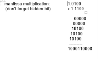
Add exponents:
always add true exponents (otherwise the bias gets added in twice)
DIVISION
It is similar to multiplication.
do unsigned division on the mantissas (don’t forget the hidden bit)
subtract TRUE exponents
The organization of a floating point adder unit and the algorithm is given below.
|
The floating point multiplication algorithm is given below. A similar algorithm based on the steps discussed before can be used for division.
|
Fig 34 – division algorithm
|
Rounding
The floating point arithmetic operations discussed above may produce a result with more digits than can be represented in 1.M. In such cases, the result must be rounded to fit into the available number of M positions. The extra bits that are used in intermediate calculations to improve the precision of the result are called guard bits. It is only a tradeoff of hardware cost (keeping extra bits) and speed versus accumulated rounding error, because finally these extra bits have to be rounded off to conform to the IEEE standard.
Rounding Methods:
- Truncate
– Remove all digits beyond those supported
– 1.00100 -> 1.00
- Round up to the next value
– 1.00100 -> 1.01
- Round down to the previous value
– 1.00100 -> 1.00
– Differs from Truncate for negative numbers
- Round-to-nearest-even
– Rounds to the even value (the one with an LSB of 0)
– 1.00100 -> 1.00
– 1.01100 -> 1.10
– Produces zero average bias
– Default mode
A product may have twice as many digits as the multiplier and multiplicand
– 1.11 x 1.01 = 10.0011
For round-to-nearest-even, we need to know the value to the right of the LSB (round bit) and whether any other digits to the right of the round digit are 1’s (the sticky bit is the OR of these digits). The IEEE standard requires the use of 3 extra bits of less significance than the 24 bits (of mantissa) implied in the single precision representation – guard bit, round bit and sticky bit. When a mantissa is to be shifted in order to align radix points, the bits that fall off the least significant end of the mantissa go into these extra bits (guard, round, and sticky bits). These bits can also be set by the normalization step in multiplication, and by extra bits of quotient (remainder) in division. The guard and round bits are just 2 extra bits of precision that are used in calculations. The sticky bit is an indication of what is/could be in lesser significant bits that are not kept. If a value of 1 ever is shifted into the sticky bit position, that sticky bit remains a 1 (“sticks” at 1), despite further shifts.
To summarize, in his module we have discussed the need for floating point numbers, the IEEE standard for representing floating point numbers, Floating point addition / subtraction, multiplication, division and the various rounding methods.
Key takeaway
The objectives of this module are to discuss the need for floating point numbers, the standard representation used for floating point numbers and discuss how the various floating point arithmetic operations of addition, subtraction, multiplication and division are carried out.
Reference:
1. “Computer Architecture and Organization”, 3rd Edition by John P. Hayes, WCB/McGraw-Hill
2. “Computer Organization and Architecture: Designing for Performance”, 10th Edition by William Stallings, Pearson Education.
3. “Computer System Design and Architecture”, 2nd Edition by Vincent P. Heuring and Harry F. Jordan, Pearson Education.
