UNIT 2
Introduction to x86 architecture. CPU control unit design, Peripheral devices and their characteristics
The Control Unit is classified into two major categories:
- Hardwired Control
- Microprogrammed Control
The Hardwired Control organization involves the control logic to be implemented with gates, flip-flops, decoders, and other digital circuits.
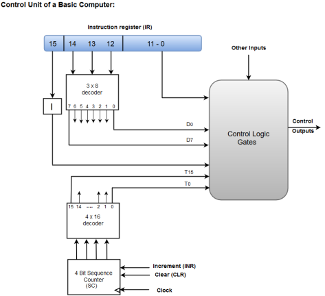
The following image shows the block diagram of a Hardwired Control organization.
|
Fig 1 – Control unit of basic computer
- A Hard-wired Control consists of two decoders, a sequence counter, and a number of logic gates.
- An instruction fetched from the memory unit is placed in the instruction register (IR).
- The component of an instruction register includes; I bit, the operation code, and bits 0 through 11.
- The operation code in bits 12 through 14 are coded with a 3 x 8 decoder.
- The outputs of the decoder are designated by the symbols D0 through D7.
- The operation code at bit 15 is transferred to a flip-flop designated by the symbol I.
- The operation codes from Bits 0 through 11 are applied to the control logic gates.
- The Sequence counter (SC) can count in binary from 0 through 15.
The Microprogrammed Control organization is implemented by using the programming approach.
In Microprogrammed Control, the micro-operations are performed by executing a program consisting of micro-instructions.
The following image shows the block diagram of a Microprogrammed Control organization.
|
Fig 2 – Microprogrammed control unit of a basic computer
- The Control memory address register specifies the address of the micro-instruction.
- The Control memory is assumed to be a ROM, within which all control information is permanently stored.
- The control register holds the microinstruction fetched from the memory.
- The micro-instruction contains a control word that specifies one or more micro-operations for the data processor.
- While the micro-operations are being executed, the next address is computed in the next address generator circuit and then transferred into the control address register to read the next microinstruction.
- The next address generator is often referred to as a micro-program sequencer, as it determines the address sequence that is read from control memory.
Key takeaway
The Hardwired Control organization involves the control logic to be implemented with gates, flip-flops, decoders, and other digital circuits.
The Microprogrammed Control organization is implemented by using the programming approach.
In Microprogrammed Control, the micro-operations are performed by executing a program consisting of micro-instructions.
Micro processing unit is synonymous to central processing unit, CPU used in traditional computer. Microprocessor (MPU) acts as a device or a group of devices which do the following tasks.
- communicate with peripherals devices
- provide timing signal
- direct data flow
- perform computer tasks as specified by the instructions in memory
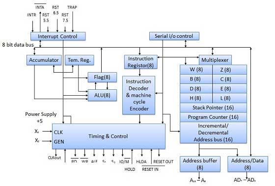
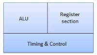
The 8085 microprocessor is an 8-bit general purpose microprocessor which is capable to address 64k of memory. This processor has forty pins, requires +5 V single power supply and a 3-MHz single-phase clock.
|
The ALU perform the computing function of microprocessor. It includes the accumulator, temporary register, arithmetic & logic circuit & and five flags. Result is stored in accumulator & flags.
|
It is an 8-bit register that is part of ALU. This register is used to store 8-bit data & in performing arithmetic & logic operation. The result of operation is stored in accumulator.
|
Fig 5 - Accumulator
Flags are programmable. They can be used to store and transfer the data from the registers by using instruction. The ALU includes five flip-flops that are set and reset according to data condition in accumulator and other registers.
- S (Sign) flag − After the execution of an arithmetic operation, if bit D7 of the result is 1, the sign flag is set. It is used to signed number. In a given byte, if D7 is 1 means negative number. If it is zero means it is a positive number.
- Z (Zero) flag − The zero flag is set if ALU operation result is 0.
- AC (Auxiliary Carry) flag − In arithmetic operation, when carry is generated by digit D3 and passed on to digit D4, the AC flag is set. This flag is used only internally BCD operation.
- P (Parity) flag − After arithmetic or logic operation, if result has even number of 1s, the flag is set. If it has odd number of 1s, flag is reset.
- C (Carry) flag − If arithmetic operation result is in a carry, the carry flag is set, otherwise it is reset.
It is basically a storage device and transfers data from registers by using instructions.
- Stack Pointer (SP) − The stack pointer is also a 16-bit register which is used as a memory pointer. It points to a memory location in Read/Write memory known as stack. In between execution of program, sometime data to be stored in stack. The beginning of the stack is defined by loading a 16-bit address in the stack pointer.
- Program Counter (PC) − This 16-bit register deals with fourth operation to sequence the execution of instruction. This register is also a memory pointer. Memory location have 16-bit address. It is used to store the execution address. The function of the program counter is to point to memory address from which next byte is to be fetched.
- Storage registers − These registers store 8-bit data during a program execution. These registers are identified as B, C, D, E, H, L. They can be combined as register pair BC, DE and HL to perform some 16 bit operations.
This unit is responsible to synchronize Microprocessor operation as per the clock pulse and to generate the control signals which are necessary for smooth communication between Microprocessor and peripherals devices. The RD bar and WR bar signals are synchronous pulses which indicates whether data is available on the data bus or not. The control unit is responsible to control the flow of data between microprocessor, memory and peripheral devices.
|
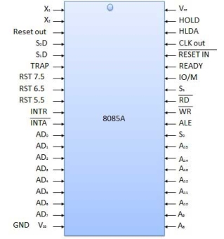
All the signal can be classified into six groups
S.N. | Group | Description |
1 | Address bus | The 8085 microprocessor has 8 signal line, A15 - A8 which are uni directional and used as a high order address bus. |
2 | Data bus | The signal line AD7 - AD0 are bi-directional for dual purpose. They are used as low order address bus as well as data bus. |
3 | Control signal and Status signal | Control Signal RD bar − It is a read control signal (active low). If it is active then memory read the data. WR bar − It is write control signal (active low). It is active when written into selected memory. Status signal ALU (Address Latch Enable) − When ALU is high. 8085 microprocessor use address bus. When ALU is low. 8085 microprocessors are use data bus. IO/M bar − This is a status signal used to differentiate between i/o and memory operations. When it is high, it indicates an i/o operation and when it is low, it indicates memory operation. S1 and S0 − These status signals, similar to i/o and memory bar, can identify various operations, but they are rarely used in small system. |
4 | Power supply and frequency signal | Vcc − +5v power supply. Vss − ground reference. X, X − A crystal is connected at these two pins. The frequency is internally divided by two operate system at 3-MHz, the crystal should have a frequency of 6-MHz. CLK out − This signal can be used as the system clock for other devices. |
5 | Externally initiated signal | INTR (i/p) − Interrupt request. INTA bar (o/p) − It is used as acknowledge interrupt. TRAP (i/p) − This is non maskable interrupt and has highest priority. HOLD (i/p) − It is used to hold the executing program. HLDA (o/p) − Hold acknowledge. READY (i/p) − This signal is used to delay the microprocessor read or write cycle until a slow responding peripheral is ready to accept or send data. RESET IN bar − When the signal on this pin goes low, the program counter is set to zero, the bus are tri-stated, & MPU is reset. RESET OUT − This signal indicate that MPU is being reset. The signal can be used to reset other devices. RST 7.5, RST 6.5, RST 5.5 (Request interrupt) − It is used to transfer the program control to specific memory location. They have higher priority than INTR interrupt. |
6 | Serial I/O ports | The 8085 microprocessor has two signals to implement the serial transmission serial input data and serial output data. |
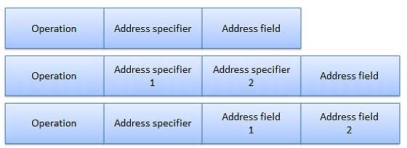
Each instruction is represented by a sequence of bits within the computer. The instruction is divided into group of bits called field. The way instruction is expressed is known as instruction format. It is usually represented in the form of rectangular box. The instruction format may be of the following types.
These are the instruction formats in which the instruction length varies on the basis of opcode & address specifiers. For Example, VAX instruction vary between 1 and 53 bytes while X86 instruction vary between 1 and 17 bytes.
|
Fig 7 – Variable instruction formats
These formats have good code density.
These instruction formats are very difficult to decode and pipeline.
In this type of instruction format, all instructions are of same size. For Example, MIPS, Power PC, Alpha, ARM.
|
Fig 8 – Fixed instruction formats
They are easy to decode & pipeline.
They don't have good code density.
In this type of instruction formats, we have multiple format length specified by opcode. For example, IBM 360/70, MIPS 16, Thumb.
|
Fig 9 – Hybrid instruction formats
These compromises between code density & instruction of these type are very easy to decode.
Addressing mode provides different ways for accessing an address to given data to a processor. Operated data is stored in the memory location, each instruction required certain data on which it has to operate. There are various techniques to specify address of data. These techniques are called Addressing Modes.
- Direct addressing mode − In the direct addressing mode, address of the operand is given in the instruction and data is available in the memory location which is provided in instruction. We will move this data in desired location.
- Indirect addressing mode − In the indirect addressing mode, the instruction specifies a register which contain the address of the operand. Both internal RAM and external RAM can be accessed via indirect addressing mode.
- Immediate addressing mode − In the immediate addressing mode, direct data is given in the operand which move the data in accumulator. It is very fast.
- Relative addressing mode − In the relative address mode, the effective address is determined by the index mode by using the program counter instead of general purpose processor register. This mode is called relative address mode.
- Index addressing mode − In the index address mode, the effective address of the operand is generated by adding a content value to the contents of the register. This mode is called index address mode.
Key takeaway
Micro processing unit is synonymous to central processing unit, CPU used in traditional computer. Microprocessor (MPU) acts as a device or a group of devices which do the following tasks.
- communicate with peripherals devices
- provide timing signal
- direct data flow
- perform computer tasks as specified by the instructions in memory
Semiconductor memory is used in any electronics assembly that uses computer processing technology. Semiconductor memory is the essential electronics component needed for any computer based PCB assembly.
In addition to this, memory cards have become commonplace items for temporarily storing data – everything from the portable flash memory cards used for transferring files, to semiconductor memory cards used in cameras, mobile phones and the like.
The use of semiconductor memory has grown, and the size of these memory cards has increased as the need for larger and larger amounts of storage is needed.
To meet the growing needs for semiconductor memory, there are many types and technologies that are used. As the demand grows new memory technologies are being introduced and the existing types and technologies are being further developed.
A variety of different memory technologies are available – each one suited to different applications. Names such as ROM, RAM, EPROM, EEPROM, Flash memory, DRAM, SRAM, SDRAM, as well as F-RAM and MRAM are available, and new types are being developed to enable improved performance.
Terms like DDR3, DDR4, DDR5 and many more are seen and these refer to different types of SDRAM semiconductor memory.
In addition to this the semiconductor devices are available in many forms – Ics for printed board assembly, USB memory cards, Compact Flash cards, SD memory cards and even solid state hard drives. Semiconductor memory is even incorporated into many microprocessor chips as on-board memory.
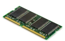
|
Fig 10 – Printed circuit board containing computer memory
Semiconductor memory: main types
There are two main types or categories that can be used for semiconductor technology. These memory types or categories differentiate the memory to the way in which it operates:
RAM - Random Access Memory: As the names suggest, the RAM or random access memory is a form of semiconductor memory technology that is used for reading and writing data in any order - in other words as it is required by the processor. It is used for such applications as the computer or processor memory where variables and other stored and are required on a random basis. Data is stored and read many times to and from this type of memory.
Random access memory is used in huge quantities in computer applications as current day computing and processing technology requires large amounts of memory to enable them to handle the memory hungry applications used today. Many types of RAM including SDRAM with its DDR3, DDR4, and soon DDR5 variants are used in huge quantities.
ROM - Read Only Memory: A ROM is a form of semiconductor memory technology used where the data is written once and then not changed. In view of this it is used where data needs to be stored permanently, even when the power is removed - many memory technologies lose the data once the power is removed.
As a result, this type of semiconductor memory technology is widely used for storing programs and data that must survive when a computer or processor is powered down. For example, the BIOS of a computer will be stored in ROM. As the name implies, data cannot be easily written to ROM. Depending on the technology used in the ROM, writing the data into the ROM initially may require special hardware. Although it is often possible to change the data, this gain requires special hardware to erase the data ready for new data to be written in.
As can be seen, these two types of memory are very different, and as a result they are used in very different ways.
Each of the semiconductor memory technologies outlined below falls into one of these two types of category. each technology offers its own advantages and is used in a particular way, or for a particular application.
Semiconductor memory technologies
There is a large variety of types of ROM and RAM that are available. Often the overall name for the memory technology includes the initials RAM or ROM and this gives a guide as to the overall type of format for the memory.
With technology moving forwards apace, not only are the established technologies moving forwards with SDRAM technology moving from DDR3 to DDR4 and then to DDR5, but Flash memory used in memory cards is also developing as are the other technologies.
In addition to this, new memory technologies are arriving on the scene and they are starting to make an impact in the market, enabling processor circuits to perform more effectively.
The different memory types or memory technologies are detailed below:
DRAM: Dynamic RAM is a form of random access memory. DRAM uses a capacitor to store each bit of data, and the level of charge on each capacitor determines whether that bit is a logical 1 or 0.
However these capacitors do not hold their charge indefinitely, and therefore the data needs to be refreshed periodically. As a result of this dynamic refreshing it gains its name of being a dynamic RAM. DRAM is the form of semiconductor memory that is often used in equipment including personal computers and workstations where it forms the main RAM for the computer. The semiconductor devices are normally available as integrated circuits for use in PCB assembly in the form of surface mount devices or less frequently now as leaded components.
EEPROM: This is an Electrically Erasable Programmable Read Only Memory. Data can be written to these semiconductor devices and it can be erased using an electrical voltage. This is typically applied to an erase pin on the chip. Like other types of PROM, EEPROM retains the contents of the memory even when the power is turned off. Also like other types of ROM, EEPROM is not as fast as RAM.
EPROM: This is an Erasable Programmable Read Only Memory. These semiconductor devices can be programmed and then erased at a later time. This is normally achieved by exposing the semiconductor device itself to ultraviolet light. To enable this to happen there is a circular window in the package of the EPROM to enable the light to reach the silicon of the device. When the PROM is in use, this window is normally covered by a label, especially when the data may need to be preserved for an extended period.
The PROM stores its data as a charge on a capacitor. There is a charge storage capacitor for each cell and this can be read repeatedly as required. However it is found that after many years the charge may leak away and the data may be lost.
Nevertheless, this type of semiconductor memory used to be widely used in applications where a form of ROM was required, but where the data needed to be changed periodically, as in a development environment, or where quantities were low.
Flash memory: Flash memory may be considered as a development of EEPROM technology. Data can be written to it and it can be erased, although only in blocks, but data can be read on an individual cell basis.
To erase and re-programme areas of the chip, programming voltages at levels that are available within electronic equipment are used. It is also non-volatile, and this makes it particularly useful. As a result Flash memory is widely used in many applications including USB memory sticks, compact Flash memory cards, SD memory cards and also now solid state hard drives for computers and many other applications.
F-RAM: Ferroelectric RAM is a random-access memory technology that has many similarities to the standard DRAM technology. The major difference is that it incorporates a ferroelectric layer instead of the more usual dielectric layer and this provides its non-volatile capability. As it offers a non-volatile capability, F-RAM is a direct competitor to Flash.
MRAM: This is Magneto-resistive RAM, or Magnetic RAM. It is a non-volatile RAM memory technology that uses magnetic charges to store data instead of electric charges.
Unlike technologies including DRAM, which require a constant flow of electricity to maintain the integrity of the data, MRAM retains data even when the power is removed. An additional advantage is that it only requires low power for active operation. As a result this technology could become a major player in the electronics industry now that production processes have been developed to enable it to be produced.
P-RAM / PCM: This type of semiconductor memory is known as Phase change Random Access Memory, P-RAM or just Phase Change memory, PCM. It is based around a phenomenon where a form of chalcogenide glass changes is state or phase between an amorphous state (high resistance) and a polycrystalline state (low resistance). It is possible to detect the state of an individual cell and hence use this for data storage. Currently this type of memory has not been widely commercialised, but it is expected to be a competitor for flash memory.
PROM: This stands for Programmable Read Only Memory. It is a semiconductor memory which can only have data written to it once - the data written to it is permanent. These memories are bought in a blank format and they are programmed using a special PROM programmer.
Typically a PROM will consist of an array of fuseable links some of which are "blown" during the programming process to provide the required data pattern.
SDRAM: Synchronous DRAM. This form of semiconductor memory can run at faster speeds than conventional DRAM. It is synchronised to the clock of the processor and is capable of keeping two sets of memory addresses open simultaneously. By transferring data alternately from one set of addresses, and then the other, SDRAM cuts down on the delays associated with non-synchronous RAM, which must close one address bank before opening the next.
Within the SDRAM family there are several types of memory technologies that are seen. These are referred to by the letters DDR - Double Data Rate. DDR4 is currently the latest technology, but this is soon to be followed by DDR5 which will offer some significant improvements in performance.
SRAM: Static Random Access Memory. This form of semiconductor memory gains its name from the fact that, unlike DRAM, the data does not need to be refreshed dynamically.
These semiconductor devices are able to support faster read and write times than DRAM (typically 10 ns against 60 ns for DRAM), and in addition its cycle time is much shorter because it does not need to pause between accesses. However they consume more power, they are less dense and more expensive than DRAM. As a result of this SRAM is normally used for caches, while DRAM is used as the main semiconductor memory technology.
Semiconductor memory technology is developing at a fast rate to meet the ever growing needs of the electronics industry. Not only are the existing technologies themselves being developed, but considerable amounts of research are being invested in new types of semiconductor memory technology.
In terms of the memory technologies currently in use, SDRAM versions like DDR4 are being further developed to provide DDR5 which will offer significant performance improvements. In time, DDR5 will be developed to provide the next generation of SDRAM.
Other forms of memory are seen around the home in the form of USB memory sticks, Compact Flash, CF cards or SD memory cards for cameras and other applications as well as solid state hard drives for computers.
The semiconductor devices are available in a wide range of formats to meet the differing PCB assembly and other needs.
Memory Organisation
The memory is organized in the form of a cell, each cell is able to be identified with a unique number called address. Each cell is able to recognize control signals such as “read” and “write”, generated by CPU when it wants to read or write address. Whenever CPU executes the program there is a need to transfer the instruction from the memory to CPU because the program is available in memory. To access the instruction CPU generates the memory request.
Memory Request:
Memory request contains the address along with the control signals. For Example, When inserting data into the stack, each block consumes memory (RAM) and the number of memory cells can be determined by the capacity of a memory chip.
Example: Find the total number of cells in 64k*8 memory chip.
Size of each cell = 8
Number of bytes in 64k = (2^6)*(2^10)
Therefore,
the total number of cells = 2^16 cells
With the number of cells, the number of address lines required to enable one cell can be determined.
Word Size:
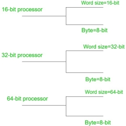
It is the maximum number of bits that a CPU can process at a time and it depends upon the processor. Word size is a fixed size piece of data handled as a unit by the instruction set or the hardware of a processor.
|
Fig 11 - Example
Word size varies as per the processor architectures because of generation and the present technology, it could be low as 4-bits or high as 64-bits depending on what a particular processor can handle. Word size is used for a number of concepts like Addresses, Registers, Fixed-point numbers, Floating point numbers.
Key takeaway
Semiconductor memory is used in any electronics assembly that uses computer processing technology. Semiconductor memory is the essential electronics component needed for any computer based PCB assembly.
In addition to this, memory cards have become commonplace items for temporarily storing data - everything from the portable flash memory cards used for transferring files, to semiconductor memory cards used in cameras, mobile phones and the like.
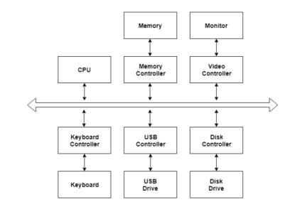
I/O devices are very important in the computer systems. They provide users the means of interacting with the system. So there is a separate I/O system devoted to handling the I/O devices.
The different Components of the I/O systems are −
There are many I/O devices handled by the operating system such as mouse, keyboard, disk drive etc. There are different device drivers that can be connected to the operating system to handle a specific device. The device controller is an interface between the device and the device driver.
A diagram to represent this is −
|
Fig 12 – I/O hardware
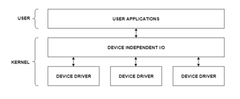
The user applications can access all the I/O devices using the device drivers, which are device specific codes. The application layer sees a common interface for all the devices.
This is illustrated using the below image −
|
Fig 13 – I/O application interface
Most of the devices are either block I/O and character I/O devices. Block devices are accessed one block at a time whereas character devices are accessed one character at a time.
The I/O software contains the user level libraries and the kernel modules. The libraries provide the interface to the user program to perform input and output. The kernel modules provide the device drivers that interact with the device controllers.
The I/O software should be device independent so that the programs can be used for any I/O device without specifying it in advance. For example - A program that reads a file should be able the read the file on a hard disk, floppy disk, CD-ROM etc. without having to change the program each time.
Key takeaway
I/O devices are very important in the computer systems. They provide users the means of interacting with the system. So there is a separate I/O system devoted to handling the I/O devices.
The method that is used to transfer information between internal storage and external I/O devices is known as I/O interface. The CPU is interfaced using special communication links by the peripherals connected to any computer system. These communication links are used to resolve the differences between CPU and peripheral. There exist special hardware components between CPU and peripherals to supervise and synchronize all the input and output transfers that are called interface units.
The binary information that is received from an external device is usually stored in the memory unit. The information that is transferred from the CPU to the external device is originated from the memory unit. CPU merely processes the information but the source and target is always the memory unit. Data transfer between CPU and the I/O devices may be done in different modes.
Data transfer to and from the peripherals may be done in any of the three possible ways
- Programmed I/O.
- Interrupt- initiated I/O.
- Direct memory access (DMA).
Now let’s discuss each mode one by one.
- Programmed I/O: It is due to the result of the I/O instructions that are written in the computer program. Each data item transfer is initiated by an instruction in the program. Usually the transfer is from a CPU register and memory. In this case it requires constant monitoring by the CPU of the peripheral devices.
Example of Programmed I/O: In this case, the I/O device does not have direct access to the memory unit. A transfer from I/O device to memory requires the execution of several instructions by the CPU, including an input instruction to transfer the data from device to the CPU and store instruction to transfer the data from CPU to memory. In programmed I/O, the CPU stays in the program loop until the I/O unit indicates that it is ready for data transfer. This is a time consuming process since it needlessly keeps the CPU busy. This situation can be avoided by using an interrupt facility. This is discussed below.
2. Interrupt- initiated I/O: Since in the above case we saw the CPU is kept busy unnecessarily. This situation can very well be avoided by using an interrupt driven method for data transfer. By using interrupt facility and special commands to inform the interface to issue an interrupt request signal whenever data is available from any device. In the meantime, the CPU can proceed for any other program execution. The interface meanwhile keeps monitoring the device. Whenever it is determined that the device is ready for data transfer it initiates an interrupt request signal to the computer. Upon detection of an external interrupt signal the CPU stops momentarily the task that it was already performing, branches to the service program to process the I/O transfer, and then return to the task it was originally performing.
Note: Both the methods programmed I/O and Interrupt-driven I/O require the active intervention of the
processor to transfer data between memory and the I/O module, and any data transfer must transverse
a path through the processor. Thus both these forms of I/O suffer from two inherent drawbacks.
- The I/O transfer rate is limited by the speed with which the processor can test and service a
device. - The processor is tied up in managing an I/O transfer; a number of instructions must be executed
for each I/O transfer.
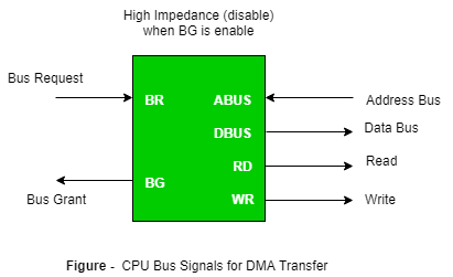
- Direct Memory Access: The data transfer between a fast storage media such as magnetic disk and memory unit is limited by the speed of the CPU. Thus we can allow the peripherals directly communicate with each other using the memory buses, removing the intervention of the CPU. This type of data transfer technique is known as DMA or direct memory access. During DMA the CPU is idle and it has no control over the memory buses. The DMA controller takes over the buses to manage the transfer directly between the I/O devices and the memory unit.
|
Fig 14 – CPU bus signals for DMA Transfer
Bus Request: It is used by the DMA controller to request the CPU to relinquish the control of the buses.
Bus Grant: It is activated by the CPU to Inform the external DMA controller that the buses are in high impedance state and the requesting DMA can take control of the buses. Once the DMA has taken the control of the buses it transfers the data. This transfer can take place in many ways.
Types of DMA transfer using DMA controller:
Burst Transfer:
DMA returns the bus after complete data transfer. A register is used as a byte count, being decremented for each byte transfer, and upon the byte count reaching zero, the DMAC will release the bus. When the DMAC operates in burst mode, the CPU is halted for the duration of the data
transfer.
Steps involved are:
- Bus grant request time.
- Transfer the entire block of data at transfer rate of device because the device is usually slow than the speed at which the data can be transferred to CPU.
- Release the control of the bus back to CPU So, total time taken to transfer the N bytes = Bus grant request time + (N) * (memory transfer rate) + Bus release control time.
Where,
X µsec =data transfer time or preparation time (words/block)
Y µsec =memory cycle time or cycle time or transfer time (words/block)
% CPU idle (Blocked)=(Y/X+Y)*100
% CPU Busy=(X/X+Y)*100
Cyclic Stealing:
An alternative method in which DMA controller transfers one word at a time after which it must return the control of the buses to the CPU. The CPU delays its operation only for one memory cycle to allow the direct memory I/O transfer to “steal” one memory cycle.
Steps Involved are:
- Buffer the byte into the buffer
- Inform the CPU that the device has 1 byte to transfer (i.e. bus grant request)
- Transfer the byte (at system bus speed)
- Release the control of the bus back to CPU.
Before moving on transfer next byte of data, device performs step 1 again so that bus isn’t tied up and the transfer won’t depend upon the transfer rate of device. So, for 1 byte of transfer of data, time taken by using cycle stealing mode (T). = time required for bus grant + 1 bus cycle to transfer data + time required to release the bus, it will be N x T
In cycle stealing mode we always follow pipelining concept that when one byte is getting transferred then Device is parallel preparing the next byte. “The fraction of CPU time to the data transfer time” if asked then cycle stealing mode is used.
Where,
X µsec =data transfer time or preparation time
(words/block)
Y µsec =memory cycle time or cycle time or transfer
time (words/block)
% CPU idle (Blocked) =(Y/X)*100
% CPU busy=(X/Y)*100
Interleaved mode: In this technique, the DMA controller takes over the system bus when the microprocessor is not using it. An alternate half cycle i.e. half cycle DMA + half cycle processor.
Key takeaway
The method that is used to transfer information between internal storage and external I/O devices is known as I/O interface. The CPU is interfaced using special communication links by the peripherals connected to any computer system. These communication links are used to resolve the differences between CPU and peripheral. There exists special hardware components between CPU and peripherals to supervise and synchronize all the input and output transfers that are called interface units.
In Input Output Transfer Techniques, the system requires the transfer of data between external circuitry and the microprocessor. In this section, we will discuss different ways of I/O transfer.
1. Program controlled I/O or Polling control.
2. Interrupt program controlled I/O or interrupt driven I/O.
3. Hardware controlled I/O.
4. I/O controlled by Handshake signals.
5. I/O controlled by ready signal.
1.Program controlled I/O or Polling control:
In program controlled I/O, the transfer of data is completely under the control of the microprocessor program. This means that the data transfer takes place only when an Input Output Transfer Techniques instruction executed. In most of the cases it is necessary to check whether the device is ready for data transfer or not. To check this, microprocessor polls the status bit associated with the I/O device.
2.Interrupt program controlled I/O or Interrupt driven I/O:
In interrupt program-controlled approach, when a peripheral is ready to transfer data, it sends an interrupt signal to the microprocessor. This indicates that the Input Output Transfer Techniques is initiated by the external I/O device. When interrupted, the microprocessor stops the execution of the program and transfers the program control to an interrupt service routine. This interrupt service routine performs the data transfer. After the data transfer, it returns control to the main program at the point it was interrupted.
To increase the speed of data transfer between memory and I/O, the hardware controlled I/O is used. It is commonly referred to as direct memory access (DMA). The hardware which controls this data transfer is commonly known as DMA controller. The DMA controller sends a HOLD signal, to the microprocessor to initiate data transfer. In response to HOLD signal microprocessor releases its data, address and control buses to the DMA controller. Then the data transfer is controlled at high speed by the DMA controller without the intervention of the microprocessor. After data transfer, DMA controller sends low on the HOLD pin, which gives the control of data, address, and control buses back to the microprocessor. This type of data transfer is used for large data transfers. This technique is explained in more details in chapter 8.
4.I/O Control by handshake signals:
The handshake signals are used to ensure the readiness of the I/O device and to synchronize the timing of the data transfer. In this data transfer, the status of handshaking signals are checked between the microprocessor and an I/O device and when both are ready, the actual data is transferred.
5. I/O control by READY signal:
This technique is used to transfer data between slower I/O device and the microprocessor. In some applications, speed of I/O system is not compatible with the microprocessor’s timings. This means that it takes longer time to read/write data. In such situations, the microprocessor has to confirm whether a peripheral is ready to transfer data or not. If READY pin is high, the peripheral is ready otherwise 8085 enters WAIT State or WAIT States. These WAIT states elongate the read/write cycle timings and prepare 8085 microprocessors to communicate with slower I/O devices.
Key takeaway
In Input Output Transfer Techniques, the system requires the transfer of data between external circuitry and the microprocessor. In this section, we will discuss different ways of I/O transfer.
1. Program controlled I/O or Polling control.
2. Interrupt program controlled I/O or interrupt driven I/O.
3. Hardware controlled I/O.
4. I/O controlled by Handshake signals.
5. I/O controlled by ready signal.
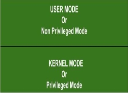
In any Operating System, it is necessary to have Dual Mode Operation to ensure protection and security of the System from unauthorized or errant users . This Dual Mode separates the User Mode from the System Mode or Kernel Mode.
|
What are Privileged Instructions?
The Instructions that can run only in Kernel Mode are called Privileged Instructions.
Privileged Instructions possess the following characteristics:
(i) If any attempt is made to execute a Privileged Instruction in User Mode, then it will not be executed and treated as an illegal instruction. The Hardware traps it to the Operating System.
(ii) Before transferring the control to any User Program, it is the responsibility of the Operating System to ensure that the Timer is set to interrupt. Thus, if the timer interrupts then the Operating System regains the control.
Thus, any instruction which can modify the contents of the Timer is a Privileged Instruction.
(iii) Privileged Instructions are used by the Operating System in order to achieve correct operation.
(iv) Various examples of Privileged Instructions include:
- I/O instructions and Halt instructions
- Turn off all Interrupts
- Set the Timer
- Context Switching
- Clear the Memory or Remove a process from the Memory
- Modify entries in Device-status table
What are Non-Privileged Instructions?
The Instructions that can run only in User Mode are called Non-Privileged Instructions.
Various examples of Non-Privileged Instructions include:
- Reading the status of Processor
- Reading the System Time
- Generate any Trap Instruction
- Sending the final printout of Printer
Also, it is important to note that in order to change the mode from Privileged to Non-Privileged, we require a Non-Privileged Instruction that does not generate any interrupt.
Key takeaway
(i) If any attempt is made to execute a Privileged Instruction in User Mode, then it will not be executed and treated as an illegal instruction. The Hardware traps it to the Operating System.
(ii) Before transferring the control to any User Program, it is the responsibility of the Operating System to ensure that the Timer is set to interrupt. Thus, if the timer interrupts then the Operating System regains the control.
Thus, any instruction which can modify the contents of the Timer is a Privileged Instruction.
Various examples of Non-Privileged Instructions include:
- Reading the status of Processor
- Reading the System Time
- Generate any Trap Instruction
- Sending the final printout of Printer
Exceptions and interrupts are unexpected events which will disrupt the normal flow of execution of instruction (that is currently executing by processor). An exception is an unexpected event from within the processor. Interrupt is an unexpected event from outside the process.
Whenever an exception or interrupt occurs, the hardware starts executing the code that performs an action in response to the exception. This action may involve killing a process, outputting an error message, communicating with an external device, or horribly crashing the entire computer system by initiating a “Blue Screen of Death” and halting the CPU. The instructions responsible for this action reside in the operating system kernel, and the code that performs this action is called the interrupt handler code. Now, We can think of handler code as an operating system subroutine. Then, After the handler code is executed, it may be possible to continue execution after the instruction where the execution or interrupt occurred.
Exception and Interrupt Handling:
Whenever an exception or interrupt occurs, execution transition from user mode to kernel mode where the exception or interrupt is handled. In detail, the following steps must be taken to handle an exception or interrupts.
While entering the kernel, the context (values of all CPU registers) of the currently executing process must first be saved to memory. The kernel is now ready to handle the exception/interrupt.
- Determine the cause of the exception/interrupt.
- Handle the exception/interrupt.
When the exception/interrupt have been handled the kernel performs the following steps:
- Select a process to restore and resume.
- Restore the context of the selected process.
- Resume execution of the selected process.
At any point in time, the values of all the registers in the CPU defines the context of the CPU. Another name used for CPU context is CPU state.
The exception/interrupt handler uses the same CPU as the currently executing process. When entering the exception/interrupt handler, the values in all CPU registers to be used by the exception/interrupt handler must be saved to memory. The saved register values can later have restored before resuming execution of the process.
The handler may have been invoked for a number of reasons. The handler thus needs to determine the cause of the exception or interrupt. Information about what caused the exception or interrupt can be stored in dedicated registers or at predefined addresses in memory.
Next, the exception or interrupt needs to be serviced. For instance, if it was a keyboard interrupt, then the key code of the key press is obtained and stored somewhere or some other appropriate action is taken. If it was an arithmetic overflow exception, an error message may be printed or the program may be terminated.
The exception/interrupt have now been handled and the kernel. The kernel may choose to resume the same process that was executing prior to handling the exception/interrupt or resume execution of any other process currently in memory.
The context of the CPU can now be restored for the chosen process by reading and restoring all register values from memory.
The process selected to be resumed must be resumed at the same point it was stopped. The address of this instruction was saved by the machine when the interrupt occurred, so it is simply a matter of getting this address and make the CPU continue to execute at this address.
Key takeaway
Exceptions and interrupts are unexpected events which will disrupt the normal flow of execution of instruction (that is currently executing by processor). An exception is an unexpected event from within the processor. Interrupt is an unexpected event from outside the process.
Whenever an exception or interrupt occurs, the hardware starts executing the code that performs an action in response to the exception. This action may involve killing a process, outputting an error message, communicating with an external device, or horribly crashing the entire computer system by initiating a “Blue Screen of Death” and halting the CPU. The instructions responsible for this action reside in the operating system kernel, and the code that performs this action is called the interrupt handler code. Now, we can think of handler code as an operating system subroutine. Then, After the handler code is executed, it may be possible to continue execution after the instruction where the execution or interrupt occurred.
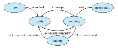
Here is process state diagram from Modern Operating Systems. Transition from running to ready happens when the scheduler picks another process.
|
Fig 15 – Transition diagram
Here is process state diagram from Operating System Concepts. What does "Interrupt" mean for transition from running to ready? Is it the same as "the scheduler picks another process" in the above?
|
Fig 16 – Process state
Key takeaway
Transition from running to ready happens when the scheduler picks another process.
What does "Interrupt" mean for transition from running to ready? Is it the same as "the scheduler picks another process" in the above?
The interface between a computer’s hardware and its software is its architecture. The architecture is described by what the computer’s instructions do, and how they are specified. Understanding how it all works requires knowledge of the structure of a computer and its assembly language.
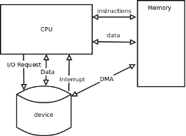
The computer is in a sense a communication system. Data is constantly being moved between the CPU, memory and the various devices. The CPU uses I/O addresses to direct data to particular devices. The devices in turn use interrupts to notify the CPU and operating system of their needs.
|
Fig 17 – CPU Process
The genesis of modern computers, however, came with the practice of storing a program in memory. according to mathematician john von neumann, for a machine to be a computer it must have the following:
- addressable memory that holds both instructions and data.
- an arithmetic logic unit.
- a program counters.
The important computer architecture components from von Neumann’s stored program control computer are:
CPU
The central processing unit is the engine of the computer that executes programs.
alu
The arithmetic logic unit is the part of the cpu that executes individual instructions involving data (operands).
register
a memory location in the CPU which holds a fixed amount of data. registers of most current systems hold 64 bits or 8 bytes of data.
pc
The Program counter, also called the instruction pointer, is a register which holds the memory address of the next instruction to be executed.
IR
The Instruction register is the register that holds the current instruction being executed.
Accumulator
A register designated to hold the result of an operation performed by the ALU.
Register File
A collection of several registers.
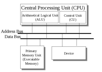
|
Fig 18 - BUS
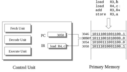
|
Fig 19 – Control Unit
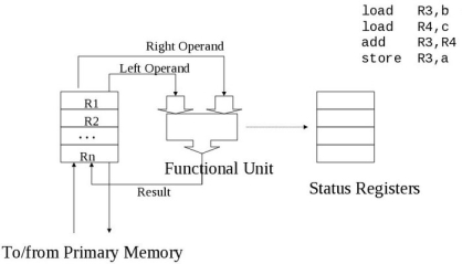
The Arithmetic Logic Unit (ALU)
|
Fig 20 - ALU
Fetch Phase
Fetch the next instruction and store it in the instruction register
Execute Phase
The ALU or I/O unit executes the instruction
- ALU does calculations
- I/O unit loads or stores data between main memory and registers
PC = <machine start address>;
IR = memory[PC];
haltFlag = CLEAR;
while(haltFlag not SET) {
execute(IR);
PC = PC + sizeof(INSTRUCT);
IR = memory[PC]; // fetch phase
};
Who is John von Neumann?
John Louis von Neumann was born 28 December 1903 in Budapest, Hungary and Died 8 February 1957 in Washington DC.
He was a brilliant mathematician, synthesizer, and promoter of the stored program concept, whose logical design of the Institute for Advanced Studies (IAS) computer became the prototype of most of its successors - the von Neumann Architecture.
Von Neumann was a child prodigy, born into a banking family in Budapest, Hungary. When only six years old he could divide eight-digit numbers in his head.
At a time of political unrest in central Europe, he was invited to visit Princeton University in 1930, and when the Institute for Advanced Studies was founded there in 1933, he was appointed to be one of the original six Professors of Mathematics, a position which he retained for the remainder of his life. By the latter years of World War II von Neumann was playing the part of an executive management consultant, serving on several national committees, applying his amazing ability to rapidly see through problems to their solutions. Through this means he was also a conduit between groups of scientists who were otherwise shielded from each other by the requirements of secrecy. He brought together the needs of the Los Alamos National Laboratory (and the Manhattan Project) with the capabilities of the engineers at the Moore School of Electrical Engineering who were building the ENIAC, and later built his own computer called the IAS machine. Several supercomputers were built by National Laboratories as copies of his machine.
Following the war, von Neumann concentrated on the development of the IAS computer and its copies around the world. His work with the Los Alamos group continued and he continued to develop the synergism between computer capabilities and the needs for computational solutions to nuclear problems related to the hydrogen bomb.
His insights into the organization of machines led to the infrastructure which is now known as the von Neumann Architecture. However, von Neumann’s ideas were not along those lines originally; he recognized the need for parallelism in computers but equally well recognized the problems of construction and hence settled for a sequential system of implementation. Through the report entitled First Draft of a Report on the EDVAC [1945], authored solely by von Neumann, the basic elements of the stored program concept were introduced to the industry.
In the 1950’s von Neumann was employed as a consultant to IBM to review proposed and ongoing advanced technology projects. One day a week, von Neumann “held court” with IBM. On one of these occasions in 1954 he was confronted with the FORTRAN concept. John Backus remembered von Neumann being unimpressed with the concept of high level languages and compilers.
Donald Gillies, one of von Neumann’s students at Princeton, and later a faculty member at the University of Illinois, recalled in the mid-1970’s that the graduates students were being “used” to hand assemble programs into binary for their early machine (probably the IAS machine). He took time out to build an assembler, but when von Neumann found out about it he was very angry, saying (paraphrased), “It is a waste of a valuable scientific computing instrument to use it to do clerical work.”
Universal Serial Bus (USB)
Universal Serial Bus (USB) is an industry standard that establishes specifications for connectors, cables and protocols for communication, connection and power supply between personal computers and their peripheral devices. There have been 3 generations of USB specifications:
1. USB 1.x
2. USB 2.0
3. USB 3.x
USB 2.0 have multiple updates and additions. The USB Implementer Forum (USB IF) currently maintains the USB standard and it was released in 1996.
USB was designed to standardize the connection of peripherals like pointing devices, keyboards, digital still and video cameras. But soon devices such as printers, portable media players, disk drives and network adaptors to personal computers used USB to communicate and to supply electric power. It is a commonplace to many devices and has largely replaced interfaces such as serial ports and parallel ports. USB connectors have replaced other types for battery chargers of portable devices with itself.
Advantages of USB –
The Universal Serial Bus was designed to simplify and improve the interface between personal computers and peripheral devices, when compared with previously existing standard or ad-hoc proprietary interfaces.
- The USB interface is self-configuring. This means that the user need not adjust settings on the device and interface for speed or data format, or configure interrupts, input/output addresses, or direct memory access channels.
- USB connectors are standardized at the host, so any peripheral can use any available receptacle. USB takes full advantage of the additional processing power that can be economically put into peripheral devices so that they can manage themselves. USB devices mostly do not have user-adjustable interface settings.
- The USB interface is hot pluggable or plug and play, meaning devices can be exchanged without rebooting the host computer. Small devices can be powered directly from the USB interface thus removing extra power supply cables.
- The USB interface defines protocols for improving reliability over previous interfaces and recovery from common errors.
- Installation of a device relying on the USB standard minimal operator action is required.
Disadvantages of USB –
- USB cables are limited in length.
- USB has a strict “tree” topology and “master-slave” protocol for addressing peripheral devices. Peripheral devices cannot interact with one another except via the host, and two hosts cannot communicate over their USB ports directly.
- Some very high speed peripheral devices require sustained speeds not available in the USB standard.
- For a product developer, use of USB requires implementation of a complex protocol and implies an intelligent controller in the peripheral device.
- Use of the USB logos on the product require annual fees and membership in the organization.
Key takeaway
The interface between a computer’s hardware and its software is its architecture. The architecture is described by what the computer’s instructions do, and how they are specified. Understanding how it all works requires knowledge of the structure of a computer and its assembly language.
The computer is in a sense a communication system. Data is constantly being moved between the CPU, memory and the various devices. The CPU uses I/O addresses to direct data to particular devices. The devices in turn use interrupts to notify the CPU and operating system of their needs.
Reference:
1. “Computer Architecture and Organization”, 3rd Edition by John P. Hayes, WCB/McGraw-Hill
2. “Computer Organization and Architecture: Designing for Performance”, 10th Edition by William Stallings, Pearson Education.
3. “Computer System Design and Architecture”, 2nd Edition by Vincent P. Heuring and Harry F. Jordan, Pearson Education.
