Module 04
Digital Electronic Principles
A digital system understands positional number system where there are few symbols called digits and these symbol represents different values depending on their position in the number.
A value of the digit is determined by using
Binary Number System
Example
Binary Number: 101112
Calculating the Decimal Equivalent of binary number −
Step | Binary Number | Decimal Number |
Step 1 | 101012 | ((1 × 24) + (0 × 23) + (1 × 22) + (1 × 21) + (1 × 20))10 |
Step 2 | 101012 | (16 + 0 + 4 + 2 + 1)10 |
Step 3 | 101012 | 2310 |
Note: 101112 is normally written as 10111.
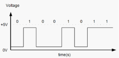
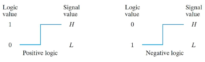
Waveforms Positive and Negative logic
In this a high-level H is represented for logic 1 and a low level L is represented for logic 0.
A digital system understands positional number system where there are few symbols called digits and these symbol represents different values depending on their position in the number.
A value of the digit is determined by using
Decimal Number System
(1×1000) + (2×100) + (3×10) + (4×l)
(1×10³) + (2×10²) + (3×101) + (4×l00)
1000 + 200 + 30 + 1
1234
S.N. | Number System & Description |
1 | Binary Number System Base 2. Digits used: 0 and 1 |
2 | Octal Number System Base 8. Digits used: 0 to 7 |
3 | Hexa Decimal Number System Base 16. Digits used: 0 to 9, Letters used: A- F |
Binary Number System
Example
Calculating the Decimal Equivalent of binary number −
Step | Binary Number | Decimal Number |
Step 1 | 101012 | ((1 × 24) + (0 × 23) + (1 × 22) + (1 × 21) + (1 × 20))10 |
Step 2 | 101012 | (16 + 0 + 4 + 2 + 1)10 |
Step 3 | 101012 | 2310 |
Note: 101112 is normally written as 10111.
2. Decimal Number: 2710
Calculating Binary Equivalent −
Step | Operation | Result | Remainder |
Step 1 | 27 / 2 | 13 | 1 |
Step 2 | 13 / 2 | 6 | 1 |
Step 3 | 6 / 2 | 3 | 0 |
Step 4 | 3 / 2 | 1 | 1 |
Step 5 | 1 / 2 | 0 | 1 |
Hence, the remainders are arranged in the reverse order and we get:
Decimal Number − 2710 = Binary Number − 110112.
It is an essential part of all the digital calculations.
Binary Addition
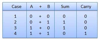
Fig. Rules of Binary addition
In fourth step, a sum (1 + 1 = 10) i.e. 0 is written in the given column and a carry of 1 over to the next column is done.
For Example −
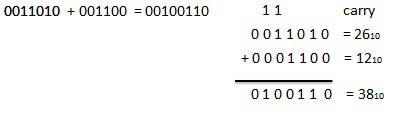
Fig. Binary addition
Binary Subtraction
Subtraction and Borrow, these are the two words that will be used very frequently for binary subtraction. There rules of binary subtraction are:
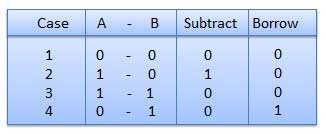
Fig. Rules of Binary Subtraction
For Example
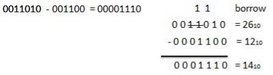
Fig. Binary subtraction
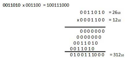
Binary Multiplication
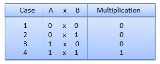
Fig. Rules of Binary Multiplication (Ref. 1)
For Example
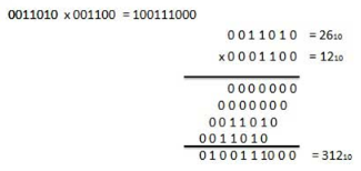
Fig. Binary Multiplication
Binary Division
For Example
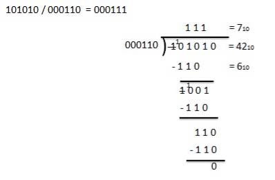
Fig. Binary Division
The basic gates are namely AND gate, OR gate & NOT gate.
AND gate
It is a digital circuit that consists of two or more inputs and a single output which is the logical AND of all those inputs. It is represented with the symbol ‘.’.
The following is the truth table of 2-input AND gate.
A | B | Y = A.B |
0 | 0 | 0 |
0 | 1 | 0 |
1 | 0 | 0 |
1 | 1 | 1 |
Here A, B are the inputs and Y is the output of two input AND gate.
If both inputs are ‘1’, then only the output, Y is ‘1’. For remaining combinations of inputs, the output, Y is ‘0’.
The figure below shows the symbol of an AND gate, which is having two inputs A, B and one output, Y.

Fig. : AND gate (ref. 1)
Timing Diagram:
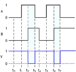
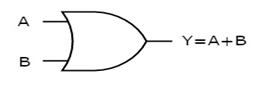
OR gate
It is a digital circuit which has two or more inputs and a single output which is the logical OR of all those inputs. It is represented with the symbol ‘+’.
The truth table of 2-input OR gate is:
A | B | Y = A + B |
0 | 0 | 0 |
0 | 1 | 1 |
1 | 0 | 1 |
1 | 1 | 1 |
Here A, B are the inputs and Y is the output of two input OR gate.
When both inputs are ‘0’, then only the output, Y is ‘0’. For remaining combinations of inputs, the output, Y is ‘1’.
The figure below shows the symbol of an OR gate, which is having two inputs A, B and one output, Y.
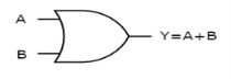
Fig. : OR gate (ref. 1)
Timing Diagram:
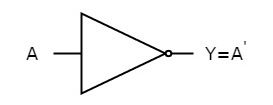
NOT gate
It is a digital circuit that has one input and one output. Here the output is the logical inversion of input. Hence, it is also called as an inverter.
The truth table of NOT gate is:
A | Y = A’ |
0 | 1 |
1 | 0 |
Here A and Y are the corresponding input and output of NOT gate. When A is ‘0’, then, Y is ‘1’. Similarly, when, A is ‘1’, then, Y is ‘0’.
The figure below shows the symbol of NOT gate, which has one input, A and one output, Y.
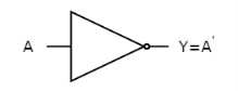
Fig. : NOT gate (ref. 1)
Timing Diagram:
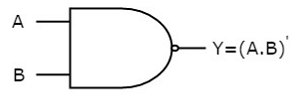
NAND gate
It is a digital circuit which has two or more inputs and single output and it is the inversion of logical AND gate.
The truth table of 2-input NAND gate is:
A | B | Y = (A.B)’ |
0 | 0 | 1 |
0 | 1 | 1 |
1 | 0 | 1 |
1 | 1 | 0 |
Here A, B are the inputs and Y is the output of two input NAND gate. When both inputs are ‘1’, then the output, Y is ‘0’. If at least one of the input is zero, then the output, Y is ‘1’. This is just the inverse of AND operation.
The image shows the symbol of NAND gate:
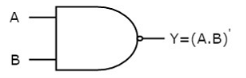
Fig.: NAND gate (ref. 1)
NAND gate works same as AND gate followed by an inverter.
Timing Diagram:
NOR gate
It is a digital circuit that has two or more inputs and a single output which is the inversion of logical OR of all inputs.
The truth table of 2-input NOR gate is:
A | B | Y = (A+B)’ |
0 | 0 | 1 |
0 | 1 | 0 |
1 | 0 | 0 |
1 | 1 | 0 |
Here A and B are the two inputs and Y is the output. If both inputs are ‘0’, then the output is ‘1’. If any one of the input is ‘1’, then the output is ‘0’. This is exactly opposite to two input OR gate operation.
The symbol of NOR gate is:
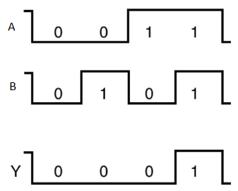
Fig.: NOR gate (ref. 1)
NOR gate works exactly same as that of OR gate followed by an inverter.
Timing Diagram:
Special Gates
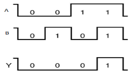
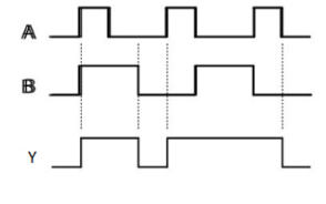
Ex-OR gate
It stands for Exclusive-OR gate. Its function varies when the inputs have even number of ones.
The truth table of 2-input Ex-OR gate is:
A | B | Y = A⊕B |
0 | 0 | 0 |
0 | 1 | 1 |
1 | 0 | 1 |
1 | 1 | 0 |
Here A, B are the inputs and Y is the output of two input Ex-OR gate. The output (Y) is zero instead of one when both the inputs are one.
Therefore, the output of Ex-OR gate is ‘1’, when only one of the two inputs is ‘1’. And it is zero, when both inputs are same.
The symbol of Ex-OR gate is as follows:

Fig.: XOR gate (ref. 1)
It is similar to that of OR gate with an exception for few combination(s) of inputs. Hence, the output is also known as an odd function.
Timing Diagram:
Ex-NOR gate
It stands for Exclusive-NOR gate. Its function is same as that of NOR gate except when the inputs having even number of ones.
The truth table of 2-input Ex-NOR gate is:
A | B | Y = A⊙B |
0 | 0 | 1 |
0 | 1 | 0 |
1 | 0 | 0 |
1 | 1 | 1 |
Here A, B are the inputs and Y is the output. It is same as Ex-NOR gate with the only modification in the fourth row. The output is 1 instead of 0, when both the inputs are one.
Hence the output of Ex-NOR gate is ‘1’, when both inputs are same and 0, when both the inputs are different.
The symbol of Ex-NOR gate is:
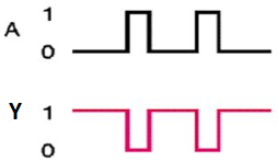
Fig.: XNOR gate (ref. 1)
It is similar to NOR gate except for few combination(s) of inputs. Here the output is ‘1’, when even number of 1 is present at the inputs. Hence is also called as an even function.
Timing Diagram:
Postulates and Basic Laws of Boolean Algebra
Here, the Boolean postulates and basic laws that are used are given underneath.
Boolean Postulates
x + 0 = x
x + 1 = 1
x + x = x
x + x’ = 1
x.1 = x
x.0 = 0
x.x = x
x.x’ = 0
Basic Laws of Boolean Algebra
Commutative Law
x + y = y + x
x.y = y.x
Associative Law
x + (y + z) = (x + y) + z
x.(y.z) = (x.y).z
Distributive Law
x.(y + z) = x.y + x.z
x + (y.z) = (x + y).(x + z)
(x + y)’ = x’.y’
(x.y)’ = x’ + y’
Numerical
f = p’qr + pq’r + pqr’ + pqr
Method 1
Given
f = p’qr + pq’r + pqr’ +pqr.
In first and second term r is common and in third and fourth terms pq is common.
So, taking out the common terms by using Distributive law we get,
⇒ f = (p’q + pq’)r + pq(r’ + r)
The terms present in first parenthesis can be simplified by using Ex-OR operation.
The terms present in second parenthesis is equal to ‘1’ using Boolean postulate we get
⇒ f = (p ⊕q)r + pq(1)
The first term can’t be simplified further.
But, the second term is equal to pq using Boolean postulate.
⇒ f = (p ⊕q)r + pq
Therefore, the simplified Boolean function is f = (p⊕q)r + pq
Method 2
Given f = p’qr + pq’r + pqr’ + pqr.
Using the Boolean postulate, x + x = x.
Hence we can write the last term pqr two more times.
⇒ f = p’qr + pq’r + pqr’ + pqr + pqr + pqr
Now using the Distributive law for 1st and 4th terms, 2nd and 5th terms, 3rdand 6th terms we get.
⇒ f = qr(p’ + p) + pr(q’ + q) + pq(r’ + r)
Using Boolean postulate, x + x’ = 1 and x.1 = x for further simplification .
⇒ f = qr(1) + pr(1) + pq(1)
⇒ f = qr + pr + pq
⇒ f = pq + qr + pr
Therefore, the simplified Boolean function is f = pq + qr + pr.
Hence we got two different Boolean functions after simplification of the given Boolean function. Functionally, these two functions are same. As per requirement, we can choose one of them.
Numerical
Find the complement of the Boolean function,
f = p’q + pq’.
Solution:
Using DeMorgan’s theorem, (x + y)’ = x’.y’ we get
⇒ f’ = (p’q)’.(pq’)’
Then by second law, (x.y)’ = x’ + y’ we get
⇒ f’ = {(p’)’ + q’}.{p’ + (q’)’}
Then by using, (x’)’=x we get
⇒ f’ = {p + q’}.{p’ + q}
⇒ f’ = pp’ + pq + p’q’ + qq’
Using x.x’=0 we get
⇒ f = 0 + pq + p’q’ + 0
⇒ f = pq + p’q’
Therefore, the complement of Boolean function, p’q + pq’ is pq + p’q’.
The following table represents the min terms and MAX terms for 2 variables.
x | y | Min terms | Max terms |
0 | 0 | m0=x’y’ | M0=x + y |
0 | 1 | m1=x’y | M1=x + y’ |
1 | 0 | m2=xy’ | M2=x’ + y |
1 | 1 | m3=xy | M3=x’ + y’ |
Canonical SoP and PoS forms
Therefore, we can express each output variable in two ways.
Canonical SoP form
Example
Considering the following truth table.
Inputs | Output | ||
P | q | r | f |
0 | 0 | 0 | 0 |
0 | 0 | 1 | 0 |
0 | 1 | 0 | 0 |
0 | 1 | 1 | 1 |
1 | 0 | 0 | 0 |
1 | 0 | 1 | 1 |
1 | 1 | 0 | 1 |
1 | 1 | 1 | 1 |
f = p’qr + pq’r + pqr’ + pqr.
f=m3+m5+m6+m7f=m3+m5+m6+m7
f=∑m(3,5,6,7)f=∑m(3,5,6,7)
Canonical PoS form
Standard SoP and PoS forms
Standard SoP form
Standard SoP of output variable can be obtained by two steps.
The same procedure is followed for other output variables too, if there is more than one output variable.
Numerical
Convert the Boolean function into Standard SoP form.
f = p’qr + pq’r + pqr’ + pqr
Solution:
Step 1 – By using the Boolean postulate, x + x = x and also writing the last term pqr two more times we get
⇒ f = p’qr + pq’r + pqr’ + pqr + pqr + pqr
Step 2 – By Using Distributive law for 1st and 4th terms, 2nd and 5th terms, 3rdand 6th terms.
⇒ f = qr(p’ + p) + pr(q’ + q) + pq(r’ + r)
Step 3 – Then Using Boolean postulate, x + x’ = 1 we get
⇒ f = qr(1) + pr(1) + pq(1)
Step 4 – hence using Boolean postulate, x.1 = x we get
⇒ f = qr + pr + pq
⇒ f = pq + qr + pr
This is the required Boolean function.
Standard PoS form
Standard PoS form of output variable is obtained by two steps.
The same procedure is followed for other output variables too.
Numerical
Convert the Boolean function into Standard PoS form.
f = (p + q + r).(p + q + r’).(p + q’ + r).(p’ + q + r)
Solution:
Step 1 – By using the Boolean postulate, x.x = x and writing the first term p+q+r two more times we get
⇒ f = (p + q + r).(p + q + r).(p + q + r).(p + q + r’).(p +q’ + r).(p’ + q + r)
Step 2 – Now by using Distributive law, x + (y.z) = (x + y).(x + z) for 1st and 4thparenthesis, 2nd and 5th parenthesis, 3rd and 6th parenthesis.
⇒ f = (p + q + rr’).(p + r + qq’).(q + r + pp’)
Step 3 − Applying Boolean postulate, x.x’=0 for simplifying of the terms present in each parenthesis.
⇒ f = (p + q + 0).(p + r + 0).(q + r + 0)
Step 4 − Using Boolean postulate, x + 0 = x we get
⇒ f = (p + q).(p + r).(q + r)
⇒ f = (p + q).(q + r).(p + r)
This is the simplified Boolean function.
Hence, both Standard SoP and Standard PoS forms are Dual to one another.
A Combinational circuit is a circuit in which we combine the different gates. For example, encoder, decoder, multiplexer, demultiplexer etc. Some of the characteristics are as follows −
Block diagram
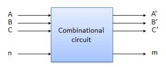
Fig. : Combinational circuit (ref.2 )
Block diagram
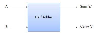
Fig. : Half adder (ref. 2)
Truth Table
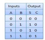
Circuit Diagram
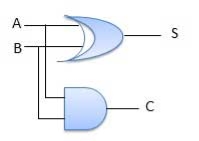
Fig : Half adder (ref. 2)
B. Full Adder
Block diagram
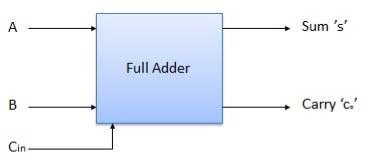
Fig.: Full adder (ref. 2)
Truth Table
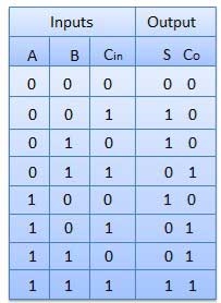
Circuit Diagram
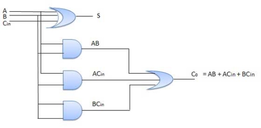
Fig.: Full adder (ref. 2)
References:
1. Electronic Devices Circuit Theory - by Rober L. Boylestad 11th Edition, Pearson Publication, 2014
2. Microelectronic Circuits by A. S. Sedra and Kenneth C. Smith 7th Edition, Oxford University Press. 2017
3. Digital Design by M. Morris Mano, 5th Edition, Pearson Publication, 2016.


