UNIT 3
LASER AND FIBRE OPTICS
The addition of a discrete amount of energy known as excitation energy added to a system such as an atomic nucleus, an atom, or a molecule that results in its alteration, generally from the condition of lowest energy (ground state) to one of higher energy (excited state).This process is called excitation.
In nuclear, atomic, and molecular systems, the excited states are not continuously distributed but have only certain discrete energy values. Thus, external energy (excitation energy) can be absorbed only in correspondingly discrete amounts.
Thus, in a hydrogen atom (composed of an orbiting electron bound to a nucleus of one proton), an excitation energy of 10.2 electron volts is required to promote the electron from its ground state to the first excited state. A different excitation energy (12.1 electron volts) is needed to raise the electron from its ground state to the second excited state.
Similarly, the protons and neutrons in atomic nuclei constitute a system that can be raised to discrete higher energy levels by supplying appropriate excitation energies. Nuclear excitation energies are roughly 1,000,000 times greater than atomic excitation energies.
The excitation energy stored in excited atoms and nuclei is radiated usually as visible light from atoms and as gamma radiation from nuclei as they return to their ground states. This energy can also be lost by collision.
The process of excitation is one of the major means by which matter absorbs pulses of electromagnetic energy (photons), such as light, and by which it is heated or ionized by the impact of charged particles, such as electrons and alpha particles. In atoms, the excitation energy is absorbed by the orbiting electrons that are raised to higher distinct energy levels. In atomic nuclei, the energy is absorbed by protons and neutrons that are transferred to excited states. In a molecule, the energy is absorbed not only by the electrons, which are excited to higher energy levels, but also by the whole molecule, which is excited to discrete modes of vibration and rotation.
Energy state also called Energy Level. Any discrete value from a set of values of total energy for a subatomic particle confined by a force to a limited space or for a system of such particles, such as an atom or a nucleus. A particular hydrogen atom, for example, may exist in any of several configurations, each having a different energy. These energy states, in their essentials, remain fixed and are referred to as stationary states.
The state of a hydrogen atom, or any sub microscopic system, however, may change from one configuration to another by emitting or absorbing a discrete amount of energy. Such configurations are also called energy levels; the atom, or system, is said to undergo a transition between two energy levels when it emits or absorbs energy. The lowest energy level of a system is called its ground state; higher energy levels are called excited states.
Interaction of external energy with atomic energy states can be understand by considering two and three level laser system.
Consider a group of electrons with two energy levels E1 and E2.
E1 is the lower energy state and E2 is the higher energy state.
N1 is the number of electrons in the energy state E1.
N2 is the number of electrons in the energy state E2.
The number of electrons per unit volume in an energy state is the population of that energy state.
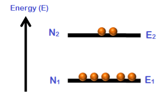
Figure: 1
Population inversion cannot be achieved in a two energy level system. Under normal conditions, the number of electrons (N1) in the lower energy state (E1) is always greater as compared to the number of electrons (N2) in the higher energy state (E2).
N1 > N2
When temperature increases, the population of higher energy state (N2) also increases. However, the population of higher energy state (N2) will never exceeds the population of lower energy state (N1).
At best an equal population of the two states can be achieved which results in no optical gain.
N1 = N2
Two energy level lasers are not possible. We cannot get population inversion in a 2. level LASER no matter how much we pump the atoms in the ground state. And since population inversion is a necessity for lasing action, we don't have two level lasers.
Therefore, we need 3 or more energy states to achieve population inversion. The greater is the number of energy states the greater is the optical gain.
There are certain substances in which the electrons once excited; they remain in the higher energy level or excited state for longer period. Such systems are called active systems or active media which are generally mixture of different elements.
When such mixtures are formed, their electronic energy levels are modified and some of them acquire special properties. Such types of materials are used to form 3-level laser or 4-level laser.
Three-level laser
The two energy levels between which lasing occur are: the lower laser energy level (E1), and the upper laser energy level (E2).
To simplify the explanation, we neglect spontaneous emission.
To achieve lasing, energy must be pumped into the system to create population inversion. So, that more atoms will be in energy level E2 than in the ground level (E1).
Atoms are pumped from the ground state(E1) to energy level E3. They stay there for an average time of 10-8 [sec], and decay (usually with a non-radiative transition) to the meta-stable energy level E2.
A schematic energy level diagram of a laser with three energy levels is shown in figure,
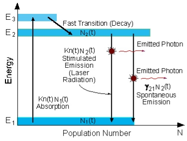
Figure 2: Energy level diagram in a three level laser
Since the lifetime of the meta-stable energy level (E2) is relatively long (of the order of 10-3 [sec], many atoms remain in this level.
If the pumping is strong enough, then after pumping more than 50% of the atoms will be in energy level E2, a population inversion exists, and lasing can occur.
In a three-level system, the laser transition ends on the ground state. The unpumped gain medium exhibits strong absorption on the laser transition. A population inversion and consequently net laser gain result only when more than half of the ions (or atoms) are pumped into the upper laser level; the threshold pump power is thus fairly high.
The population inversion can be achieved only by pumping into a higher-lying level, followed by a rapid radiative or non-radiative transfer into the upper laser level, because in this way one avoids stimulated emission caused by the pump wave. (For transitions between only two levels, simultaneous pump absorption and signal amplification cannot occur.)
An example of a three-level laser medium is ruby (Cr3+:Al203), as used by Maiman for the first laser.
Einstein’s theory of matter radiation interaction and a and b coefficients
The distribution of atoms in the two energy levels will change by absorption or emission ofradiation. Einstein introduced three empirical coefficients to quantify the change of population of the two levels.Let N1be the number of atoms per unit volume with energyE1and N2be the number of atoms per unit volume with energyE2. Let ‘n’ be the number of photons per unit volumeat frequency ‘υ’ such that hυ= E1− E2.
Then, the energy density of photons ρ(υ) =nhυ

Figure:3
When these photons interact with atoms, both upward (absorption) and downward (emission) transition occurs.
At the equilibrium the upward transitions must be equal downward transitions.
Upward Transition
Stimulated absorption rate depends upon the number of atoms available in the lowest energy state as well as the energy density photons.
We have seen above that
Stimulated absorption rate∝ N1i.e. Number of atoms in the ground state
∝ ρ(υ)i.e. Density of photons spontaneous emission
Stimulated absorption rate= B12N1ρ(υ) ………(1)
Where B12 is the Einstein coefficient of stimulated absorption.
Downward transition
The spontaneous emission rate depends up on the number of atoms present in the excited state.
Spontaneous emission rate∝ N2 i.e. number of atoms in the excited state
Spontaneous emission rate = A21N2 ………(2)
Where A21 is the Einstein coefficient of spontaneous emission.
Stimulated emission rate depends upon the number of atoms available in the excited state as well as the energy density of photons.
Stimulated emission rate ∝N2 i.e. number of atoms in the excited state
∝ρ(υ) i.e. Density of photons
Stimulated emission rate = B21N2ρ(υ) ………(3)
If the system is in equilibrium the upward transitions must be equal downward transitions.
upward transitions =downward transitions
B12N1ρ(υ) = A21N2+B21N2ρ(υ) ………(4)
B12N1ρ(υ) -B21N2ρ(υ) = A21N2
(B12N1-B21N2)ρ(υ) = A21N2
ρ(υ) = ………(5)
Divide with B21N2 in numerator and denominator in right side of the above equation,
ρ(υ) =  =
=  ………(6)
ρ(υ) =  =
=  =
= ………(7)
We know from Maxwell Boltzmann distribution law
 =
=  ………(8)
And also from Planck’s law, the radiation density
ρ(υ) =  ………(9)
Comparing the two equations (7) and (9)
 =
= and
and  =1 ………(10)
The above relations referred to as Einstein relations.
From the above equation for non degenerate energy levels the stimulated emission rate is equal to the stimulated absorption rate at the equilibrium condition.
 =
=  ………(11)
Let us discuss Einstein’s theory of interaction of electromagnetic radiation with matter. He proposed that electromagnetic radiation interacts with matter in following three steps.
Stimulated Absorption:
Let E1and E2be the energies of ground and excited states of an atom. Suppose, if a photon of energy hν=E1−E2interacts with an atom present in the ground state, the atom gets excitation form ground stateE1 to excited stateE2. This process is called stimulated absorption. Stimulated absorption rate depends upon the number of atoms available in the lowest energy state as well as the energy density photons.
Stimulated absorption rate∝Number of atoms in the ground state
∝ Density of photons Spontaneous emission
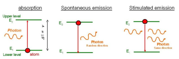
Figure:4
Spontaneous Emission:
Let E1and E2be the energies of ground and excited states of an atom. Suppose, if a photon of energy hν=E1−E2interacts with an atom present in the ground state, the atom gets excitation form ground stateE1 to excited stateE2. The excited atom does not stay in a long time in the excited state. The excited atom gets de-excitation after its life time by emitting a photon of energyhν=E1−E2. This process is called spontaneous emission. Also Spontaneous means by its own. Here excited atom comes to ground state by its own so it is named as spontaneous emission.
The spontaneous emission rate depends up on the number of atoms present in the excited state.
Spontaneous emission ∝rate number of atoms in the excited state
Stimulated Emission:
This phenomena is responsible for producing laser light. Let E1and E2be the energies of ground and excited states of an atom. Suppose, if a photon of energy hν=E1−E2interacts with an atom present in the ground state, the atom gets excitation form ground stateE1 to excited state E2. Let, a photon of energy hν=E1−E2interacts with the excited atom with in their life time; the atom gets de-excitation to ground state by emitting of another photon. These photons have same phase and it follows coherence. This phenomenon is called stimulated emission.
Stimulated emission rate depends upon the number of atoms available in the excited state as well as the energy density of photons.
Stimulated emission rate ∝ number of atoms in the excited state
∝Density of photons
Definition
The number of atoms present in the excited state or higher energy state is greater than the number of atoms present in the ground state or lower energy state is called population inversion.
Population inversion as name suggests that this is inverted phenomena. In general lower energy level is more populated that means it have more number of atoms in lower energy level as compared to higher energy level. But by pumping we will obtain a state when the number of atoms present in the higher energy state is greater than the number of atoms present in lower energy state.
Let us consider two level energy system of energies E1 and E2 as shown in figure.
Let N1 and N2 be the populations that mean number of atoms per unit volume of energy levels E1 andE2respectively.
According to Boltzmann’s distribution the population of an energy level E, at temperature T is given by
Ni=N0
Where N0 is the population of the lower level or ground state and k is the Boltzmann’s constant.
From the above relation, the population of energy levels E1 andE2 are
N1=N0
N2=N0
At ordinary conditionsN1>N2 i.e., the population in the ground or lower state is always greater than the population in the excited or higher states. The stage of making, population of higher energy level is greater than the population of lower energy level is called population inversion i.e. N1< N2
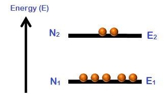
Figure 5
When population inversion method is used to enforce more and more atoms to give up photons. This initiates a chain reaction and releasing massive amount of energy.
This results in rapid build-up of energy of emitting one particular wavelength traveling coherently in fixed direction. This process is called amplification by stimulated emission using population inversion.
This population inversion situation is essential for a laser action. For any stimulated emission, It is necessary that the upper energy level or meta stable state should have a long life time, i.e., the atoms should pause at the meta stable state for more time than at the lower level.
Thus for laser action, pumping mechanism (exciting with external source) maintain a higher population of atoms in the upper energy level relative to that in the lower level.
A system in which population inversion is achieved is called as an active system. The method of raising the particles from lower energy state to higher energy state is called pumping.
The process of achieving of population inversion is called pumping.
This can be done by number of ways.
The most commonly used pumping methods are
Optical pumping As the name suggests, in this method, light is used to supply energy to the laser medium. Optical pumping is used in solid laser. Xenon flash tubes are used for optical pumping. Since these materials have very broad band absorption, sufficient amount of energy is absorbed from the emission band of flash lamp and population inversion is created. So xenon flash lamp is used to produce more electrons in the higher energy level of the laser medium.
Examples of optically pumped lasers are ruby, Nd: YAG Laser(Neodymium: Yttrium Aluminium Garnet).
Electrical discharge pumping Electrical discharge pumping is used in gas lasers. Since gas lasers have very narrow absorption band pumping then any flash lamp is not possible. Electric discharge refers to flow of electrons or electric current through a gas, liquid or solid.
In this method of pumping, electric discharge acts as the pump source or energy source. A high voltage electric discharge (flow of electrons, electric charge, or electric current) is passed through the laser medium or gas. The intense electric field accelerates the electrons to high speeds and they collide with neutral atoms in the gas. As a result, the electrons in the lower energy state gains sufficient energy from external electrons and jumps into the higher energy state
Examples of Electrical discharge pumped lasers are He-Ne laser, CO2 laser, argon-ion laser etc.
Chemical pumping Chemical reaction may also result in excitation and hence creation of population inversion in few systems.
If an atom or a molecule is produced through some chemical reaction and remains in an excited state at the time of production, then it can be used for pumping. The hydrogen fluoride molecule is produced in an excited state when hydrogen and fluorine gas chemically combine. The number of produced excited atoms or molecules is greater than the number of normal state atoms or molecules. Thus, population inversion is achieved.
Examples H2 + F2→ 2HF, in this chemical reaction, hydrogen (H2) and fluorine (F2) molecules are chemically combined to produce hydrogen fluoride molecule (2HF) in an excited state.
Thermal Pumping: Sometimes we can achieve population inversion by heating the laser medium. In thermal pumping, heat acts as the pump source or energy source. In this method, population inversion is achieved by supplying heat into the laser medium.
When heat energy is supplied to the laser medium, the lower energy state electrons gains sufficient energy and jumps into the higher energy level.
The process of achieving population inversion in thermal pumping is almost similar to the optical pumping or electric discharge method, except that in this method heat is used as pump source instead of light or electric discharge.
Injection current pumping In semiconductors, injection of current through the junction results in creates of population inversion among the minority charge carriers.
Examples of such systems are InP and GaAs.
Inelastic Atom-Atom Collisions: Like the electric discharge method, here also a high voltage electric discharge acts as a pump source. However, in this method, a combination of two types of gases, say X and Y are used. The excited state of gas X is represented as X+ whereas gas Y is represented as Y+. Both X and Y gases have the same excited states (X+ and Y+).
When high voltage electric discharge passes through a laser medium having two types of gases X and Y, the lower energy state electrons in gas X will move to the excited state X+ similarly the lower energy state electrons in gas Y moves to the excited state Y+.
Initially, during electric discharge, the lower energy state electrons in gas X or atom X gets excited to X+ due to continuous collision with electrons. The excited state electrons in gas X+ now collide with the lower energy state electrons in gas Y. As a result, the lower energy state electrons in gas Y gains sufficient energy and jump into the excited state Y+. This method is used in the Helium–Neon (He-Ne) laser.
Every LASER consists of three basic components. These are –
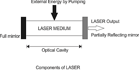 Figure: 6
The active medium is excited by the external energy source(pump source) to produce the population inversion. In the gain medium that spontaneous and stimulated emission of photons takes place, leading to the phenomenon of optical gain, or amplification. Semiconductors, organic dyes, gases (He, Ne, CO2, etc), solid materials (YAG, sapphire (ruby) etc.) are usually used as lasing materials and often LASERs are named for the ingredients used as a medium.
The excitation source, pump source provides energy which is needed for the population inversion and stimulated emission to the system. Pumping can be done in two ways – electrical discharge method and optical method. Examples of pump sources are electrical discharges, flash lamps, arc lamps, light from another laser, chemical reactions etc.
Resonator guide basically provides the guidance about the simulated emission process. It is induced by high-speed photons. Finally, a laser beam will be generated.
In most of the systems, it consists of two mirrors. One mirror is fully reflective and other is partially reflective. Both the mirrors are set up on optic axis, parallel to each other. The active medium is used in the optical cavity between the both mirrors. This arrangement only filters those photons which came along the axis and others are reflected by the mirrors back into the medium, where it may be amplified by stimulated emission.
Solid-State Lasers (Ruby Laser)
Ruby laser is a three level solid state laser and was constructed by Maiman in 1960. Ruby laser is one of the few solid-state lasers that produce visible light. It emits deep red light of wavelength 694.3 nm.
Construction
A ruby laser consists of three important elements: laser medium, the pump source and the optical resonator.
Laser Medium
Ruby (Al2O3+Cr2O3) is a crystal of Aluminium oxide, in which 0.05% of Al+3 ions are replaced by the Cr+3 ions. The colour of the rod is pink. The active medium or laser medium in the ruby rod is Cr+3 ions.In ruby laser 4cm length and 5mm diameter rod is generally used. The ruby has good thermal properties.
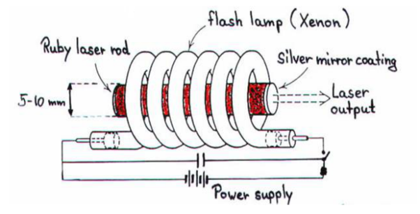
Figure: 7
The pump source
The ruby rod is surrounded by xenon flash tube, which provides the pumping light to excite the chromium ions in to upper energy levels. The ruby rod was surrounded by a helical xenon flash lamp.
We know that population inversion is required to achieve laser emission. Population inversion is the process of achieving the greater population of higher energy state than the lower energy state. In order to achieve population inversion, we need to supply energy to the laser medium i.e. to ruby crystal.
Xenon flash tube emits thousands joules of energy in few milliseconds, but only a part of that energy is utilized by the chromium ions while the rest energy heats up the apparatus. A cooling arrangement is provided to keep the experimental set up at normal temperatures.
Optical resonator
Both the ends of the rods are highly polished and made strictly parallel. The ends are silvered in such a way, one becomes partially reflected the laser beam was emitted through that end and the other end fully reflected to reflect all the rays of light striking it.
Working of ruby laser:
Consider a ruby laser medium consisting of three energy levels E1, E2, E3with N number of electrons.
We assume that the energy levels will be E1< E2< E3. The energy level E1 is known as ground state or lower energy state, the energy level E2 is known as metastable state, and the energy level E3 is known as pump state.
Let us assume that initially most of the electrons are in the lower energy state (E1) and only a tiny number of electrons are in the excited states (E2 and E3).
The energy level diagram of chromium ions is shown in figure. The chromium ions get excitation into higher energy levels by absorbing of 5500Åof wavelength radiation. The excited chromium ions stay in the level E3 for short interval of time (10-8 to 10-9 Sec). After their life time most of the chromium ions are de-excited from E3 to E1 and a few chromium ions are de-excited from E3 to E2.
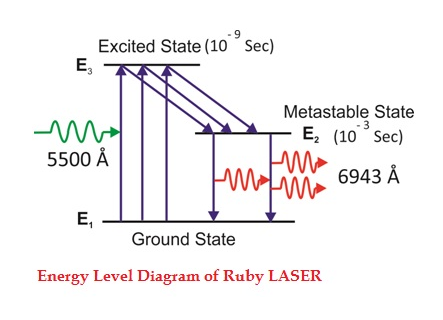
Figure: 8
The transition between E3 and E2 is non-radioactive transition i.e. the chromium ions gives their energy to the lattice in the form of heat. In the Meta stable state the life time of chromium ions is 10-3 sec. The life time of chromium ions in the Meta stable state is 105 times greater than the life time of chromium ions in higher state.
Due to the continuous working of flash lamp, the chromium ions are excited to higher state E3 and returned to E2 level. After few milliseconds the level E2 is more populated than the level E1 and hence the desired population inversion is achieved. The state of population inversion is not a stable one. The process of spontaneous transition is very high. When the excited chromium ion passes spontaneously from E3 to E2it emits one photon of wave length 6943 Å. The photon reflects back and forth by the silver ends and until it stimulates an excited chromium ion in E2 state and it to emit fresh photon in phase with the earlier photon. The process is repeated again and again until the laser beam intensity is reached to a sufficient value. When the photon beam becomes sufficient intense, it emerges through the partially silvered end of the rod. The wave length 6943 Å is in the red region of the visible spectrum.
Draw backs of ruby laser
Application of ruby laser
First He-Ne gas laser was fabricated in 1961 by Ali Javan, Bennett and Herriott at Bell Telephone Laboratories others. Helium-Neon laser is a type of gas laser in which a mixture of helium and neon gas is used as a gain medium. Helium-Neon laser is also known as He-Ne laser. The helium-neon laser was the first continuous wave laser ever constructed. The helium-neon laser operates at a wavelength of 632.8 nanometres (nm), in the red portion of the visible spectrum.
Ruby laser is a pulse laser, even it have high intense output. For continuous laser beam gas lasers are used. Using gas lasers, we can achieve highly coherence, high directionality and high monochromacity beam. The output power of the gas laser is generally in few milliwatts.
Construction
The helium-neon laser consists of three essential components:
Pump source
The gain medium of a helium-neon laser is made up of the mixture of helium and neon gas contained in a glass tube at low pressure. In He-Ne gas laser, the He and Ne gases are taken in the ratio 10:1 in the discharge tube.
Gain medium
In He-Ne laser 80cm length and 1cm diameter discharge is generally used. The out power of these lasers depends on the length of the discharge tube and pressure of the gas mixture. Therefore, in order to achieve population inversion, we need to pump electrons from lower energy state of the helium. In He-Ne laser, neon atoms are the active centres and have energy levels suitable for laser transitions while helium atoms help in exciting neon atoms.

Figure: 9
Resonating cavity
Two reflecting mirrors are fixed on either ends of the discharge tube, in that, one is partially reflecting and the other is fully reflecting.The fully silvered mirror will completely reflect the light whereas the partially silvered mirror will reflect most part of the light but allows some part of the light to produce the laser beam.
Working
When the electric discharge is passing through the gas mixture, the electrons accelerated towards the positive electrode. During their passage, they collide with He atoms and excite them into higher levels. 23s1 and 21s0 form ground state of He atom. In higher levels 23s1 and 21s0, the life time of He atoms is more. So there is a maximum possibility of energy transfer between He and Ne atoms through atomic collisions. When He atoms present in the levels 23s1 and 21s0collide with Ne atoms present ground state, the Ne atoms gets excitation into higher levels 4s and 5s.
Due to the continuous excitation of Ne atoms, we can achieve the population inversion between the higher levels 4s and 5s and lower levels 3p and 4p. The various transitions5s to 4p,4s to 3p and 5s to 3p leads to the emission of wavelengths 3.93μm, 1.51μm and 6328 Å or 632.8μm.
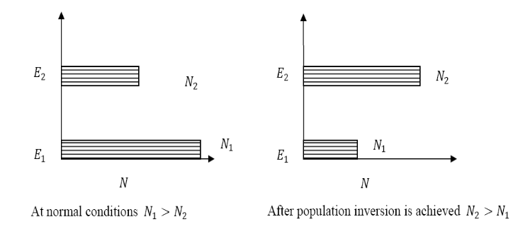
Figure: 10
The first two corresponding to the infrared region while the last wavelength is corresponding to the visible region. The Ne atoms present in the 4s level are de-excited into 3s level, by spontaneously emitting a photon of around wavelength 6000 Å. When a narrow discharge tube is used, the Ne atoms present in the level 3s collide with the walls of the tube and get de-excited to ground state energy level.
Advantages of helium-neon laser
Disadvantages of helium-neon laser
Applications of helium-neon lasers
Semiconductor Laser
It is a solid state semiconductor laser.It is specifically fabricated p-n junction diode. This diode emits laser light when it is forward biased. A semiconductor laser is a device that causes laser oscillation by flowing an electric current to semiconductor. The mechanism of light emission is the same as a light-emitting diode (LED). Light is generated by flowing the forward current to a p-n junction. In forward bias operation, the p-type layer is connected with the positive terminal and the n-type layer is connected with the negative terminal, electrons enter from the n-type layer and holes from the p-type layer. When the two meet at the junction, an electron drops into a hole and light is emitted at the time.
Semiconductor lasers represent one of the most important class of lasers in use today, not only because of the large variety of direct applications in which they are involved but also because they have found a widespread use as pumps for solid state lasers.
Semiconductor lasers require, for the active medium, a direct gap material and accordingly, the normal elemental semiconductors like Si or Gecannot be used. The majority of semiconductor-laser materials are based on a combination of elements belonging to the third group of the periodic table such as Al, Ga, In with elements of the fifth group such as N, P,As, Sb Examples include the best known GaAs as well as some ternary AlGaAs, InGaAs and quaternary InGaAsP alloys.
InGaN semiconductor lasers the best candidates for semiconductor laser emission in the very important blue-green spectral region. Semiconductor laser materials are not limited to III–V compounds, however. For the blue-green end of the spectrum we note that there are wide-gap semiconductors using a combination between elements of the second group (such as Cd and Zn) and of the sixth group (S, Se).
PRINCIPLE
When a p-n junction diode is forward biased, the electrons from n – region and the holes from the p- region cross the junction and recombine with each other.
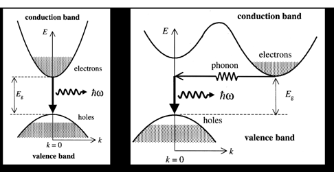
During the recombination process, the light radiation (photons) is released from a certain specified direct band gap semiconductors like Ga-As. This light radiation is known as recombination radiation.
The photon emitted during recombination stimulates other electrons and holes to recombine. As a result, stimulated emission takes place which produces laser.

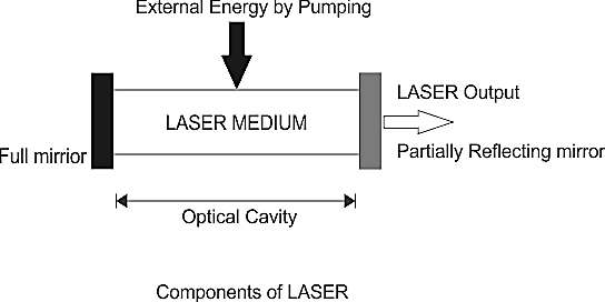
Figure: 11
CONSTRUCTION
The basic structure of a semiconductor laser is shown in Figure.The active medium is a p-n junction diode made from the single crystal of gallium arsenide. The active layer called as light emission layer sandwiched between the p- and n-type clad layers i.e. double hetero structure is formed on an n-type substrate and voltage is applied across the p-n junction from the electrodes. This crystal is cut in the form of a platter having thickness of 0.5μmm. Both edges of the active layer has mirror-like surface. When forward voltage is applied, electrons combine with holes at the p-n junction, and emit the light.
This light is not a laser yet; it is confined within the active layer because the refractive index of the clad layers is lower than that of the active layer. In addition both ends of the active layer act as a reflecting mirror where the light reciprocates in the active layer. Then, the light is amplified by the stimulated emission process and laser oscillation is generated.
The photon emission is stimulated in a very thin layer of PN junction (in order of few microns). The electrical voltage is applied to the crystal through the electrode fixed on the upper surface. The end faces of the junction diode are well polished and parallel to each other. They act as an optical resonator through which the emitted light comes out.
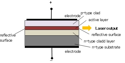
Figure: 12
WORKING
When the PN junction is forward biased with large applied voltage, the electrons and holes are injected into junction region in considerable concentration
The region around the junction contains a large amount of electrons in the conduction band and a large amount of holes in the valence band.
If the population density is high, a condition of population inversion is achieved. The electrons and holes recombine with each other and this recombination’s produce radiation in the form of light.
When the forward – biased voltage is increased, more and more light photons are emitted and the light production instantly becomes stronger. These photons will trigger a chain of stimulated recombination resulting in the release of photons in phase.
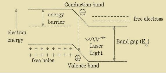
Figure: 13
The photons moving at the plane of the junction travels back and forth by reflection between two sides placed parallel and opposite to each other and grow in strength.
After gaining enough strength, it gives out the laser beam of wavelength 8400Å. The nature of output is continuous wave or pulsed output. The power output from this laser is 1mW. The wavelength of laser light is given by
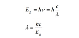
Where Eg is the band gap energy in joule.
ADVANTAGES
DISADVANTAGES
APPLICATION
OPTICAL FIBRE
A cable which is used to transmit the data through fibres (threads) or plastic (glass) is known as optical fibre cable. This cable includes a pack of glass threads which transmits modulated messages over light waves.
Principle: Optical Fibre works on the principle of Total Internal Reflection.
Total internal reflection:-
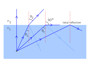
When the light ray travels from denser medium to rarer medium the refracted ray bends away from the normal. When the angle of incidence is greater than the critical angle, the refracted ray again reflects into the same medium. This phenomenon is called total internal reflection. The refracted ray bends towards the normal as the ray travels from rarer medium to denser medium. The refracted ray bends away from the normal as it travels from denser medium to rarer medium.
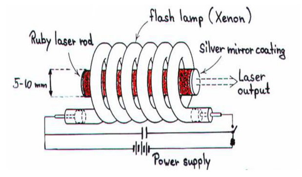
Figure 14 – Total Internal Reflection
CHARACTERISTICS OF OPTICAL FIBRE
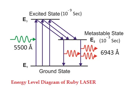
Figure 15: Optical Fibre
CONSTRUCTION OF OPTICAL FIBRE
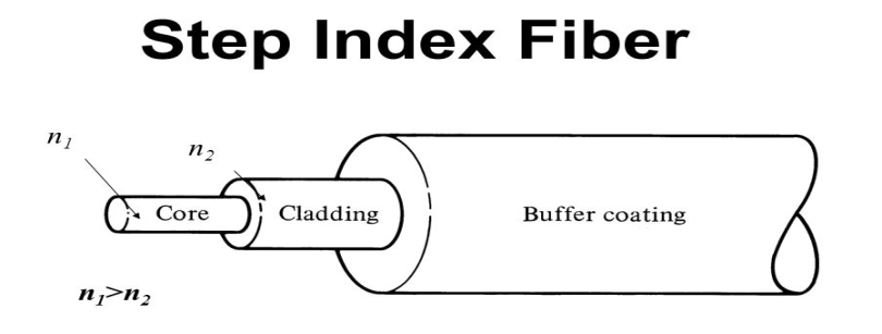
It consists of a very thin fibre of silica or glass or plastic of a high refractive index called the core. The core has a diameter of 10 um to 100 um. The core is enclosed by a cover of glass or plastic called cladding. The refractive index of the cladding is less than that of the core (which is a must condition for the working of the optical fibre). The difference between the two indicates is very small of order 10-3. The core and the cladding are enclosed in an outer protective jacket made of plastic to provide strength to the optical fibre. The refractive index can change from core to cladding abruptly (as in step-index fibre) or gradually (as in graded-index fibre).
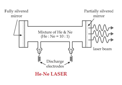
Figure16: Representation of Optical Fibre
WORKING OF OPTICAL FIBRE
When a ray of light is incident on the core of the optical fibre at a small angle, it suffers refraction and strikes the core-cladding interface, As the diameter of the fibre is very small hence the angle of incidence is greater than the critical angle. Therefore, the ray suffers total internal reflection at the core-cladding interface and strikes the opposite interface. At this interface also, the angle of incidence is greater than the critical angle, so it again suffers total internal reflection. Thus, the ray of light reaches the other end of the fibre after suffering repeated total internal reflections along the length of the fibre. At the other end, the ray suffers refraction and emerges out the optical fibre.
We can see that the light travels in the core in a guided manner. Hence the communication through the optical fibre is sometimes referred as an optical waveguide.
ACCEPTANCE ANGLE
Definition:-Acceptance angle is defined as the maximum angle of incidence at the interface of air medium and core medium for which the light ray enters into the core and travels along the interface of core and cladding.
Let n0 be the refractive indices of air
n1 be the refractive indices of core
n2 be the refractive indices of cladding
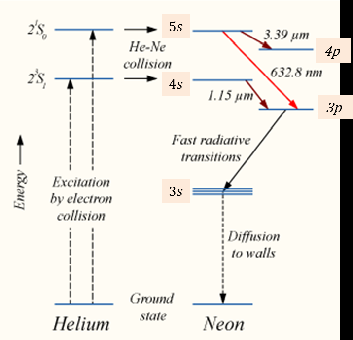
Figure: 17
Let a light ray OA is incident on the interface of air medium and core medium with an angle of incidence θ0
The light ray refracts into the core medium with an angle of refraction θ1 and the refracted ray AB is again incidenting on the interface of core and cladding with an angle of incident (90-θ1)
If (90-θ1) is equal to the critical angle of core and cladding media then the ray travels along the interface of core and cladding along the path BC. If the angle of incident at the interface of air and coreθ1<θ0 then (90-θ1) will be greater than the critical angle. Therefore,
The total internal reflection takes place.
According to Snell’s law at point A
n0Sin θ0 = n1 Sin θ1
Sin θ0= (n1 / n0) Sin θ1 ………(1)
According to Snell’s law at point B
n1Sin(90- θ1) = n2 Sin90 ………(2)
n1 Cosθ1 = n2 as(Sin90=1)
Cosθ1 = n2 /n1
Sinθ1 = (1-Cos2θ1)1/2
Sinθ1= (1- (n2 /n1)2)1/2
Sinθ1= ( n12- n22 )1/2/ n1 ………(3)
We know Sin θ0= (n1 / n0) Sin θ1 from equation (1)
Substitute the value of Sinθ1 from equation (3)
Sinθ0= (n1 / n0) *( n12- n22 )1/2/ n1
On simplification
Sinθ0= ( n12- n22 )1/2/ n0
θ0=Sin-1( n12- n22 )1/2/ n0
Acceptance Angle is θ0=Sin-1( n12- n22 )1/2/ n0 ………(4)
NUMERICAL APERTURE
Definition: -Numerical aperture is defined as the light gathering capacity of an optical fibre and it is directly proportional to the acceptance angle. Numerically it is equal to the sin of the acceptance angle.
NA = Sin(acceptance angle)
NA = Sin {Sin-1 (( n12- n22 )1/2/ n0)} from equation (4)
NA = (( n12- n22 )1/2/ n0) ………(5)
If the refractive index of the air medium is unity i.e. n0=1 put in (5)
NA = ( n12- n22 )1/2 ………(6)
Fractionalchange in refractive index
∆= (n1- n2)/ n1
n1∆ = (n1- n2) ………(7)
from equation (6), we have
NA = {( n1- n2 )( n1+n2 )}1/2
NA = { n1∆ (n1+n2 )}1/2 as n1∆ = (n1- n2) by Eq(7)
NA = { n1∆ 2n1}1/2 n1≈n2, so n1+n2 =2n1
NA = n1{2∆}1/2
This gives the relation between Numerical aperture and Fractionalchange in refractive index.
NORMALIZED FREQUENCY Or V-NUMBER
An optical fibre is characterized by one more important parameter, known as V-number which is more generally called normalized frequency of the fibre. It is given by the relation
V – number determines how many modes a fiber can support, It is given by,
V =  NA
NA
Where d is the diameter of the core,
l is the wavelength of light used
NA is the numerical aperture of the fibre.
V =
Or
V =


If V ≤ 2.405, then the fibre is single mode fibre (SMF)
If V > 2.405, then the fibre is multimode fibre (MMF)
Example: Consider a multimode step index fibre with n1 = 1.53 and n2 = 1.50 and λ= 1μm. If the core radius = 50 μm then calculate the normalized frequency of the fibre (V) and the number of guided mode.
Solution:
d = 2r = 2 x 50 x 10-6 m
V =  NA =
NA = =
= 
=94.72= normalized frequency
Total number of guided mode = M = V2/2 = 4486.
The types of optical fibres depend on the refractive index, materials used, and mode of propagation of light.
Plastic Optical Fibres: The polymethylmethacrylate is used as a core material for the transmission of the light.
Example:
Core: polymethylmethacrylate : Cladding: Co- Polymer
Core: Polystyrene : Cladding: Methyl methacrylate
Glass Fibres: It consists of extremely fine glass fibres.
Example:
Core: SiO2 Cladding: SiO2
Core: GeO2- SiO2 Cladding: SiO2
Mode of propagation:
Light propagates as electromagnetic waves through an optical fibre. All waves, having ray directions above the critical angle will be trapped within the fibre due to total internal reflection. However, all such waves do not propagate through the fibre. Only certain ray directions are allowed to propagate. The allowed directions correspond to the modes of the fibre. In simple terms, modes can be visualized as the possible number of paths of light in an optical fibre.
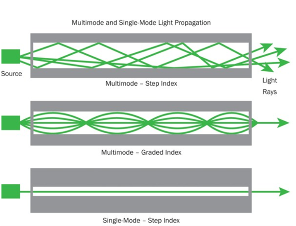
These fibres are used for long-distance transmission of signals. In general, the single mode fibres are step – index fibres. These types of fibres are made from doped silica. It has a very small core diameter so that it can allow only one mode of propagation and hence called single mode fibres.
The cladding diameter must be very large compared to the core diameter. Thus in the case of single mode fibre, the optical loss is very much reduced. The structure of a single mode fibre is given below.
Structure:
Core diameter : 5-10μm
Cladding diameter : Generally around 125μm
Protective layer : 250 to 1000μm
Numerical aperture : 0.08 to 0.10
Band width : More than 50MHz km.
Application:
Because of high bandwidth, they are used in long haul communication systems.
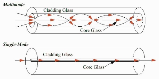
Figure: 18
These fibres are used for short-distance transmission of signals. The multi-mode fibres are useful in manufacturing both for step – index and graded index fibres. The multi-mode fibres are made by multi-component glass compounds such as Glass – Clad Glass, Silica – Clad – Silica, doped silica etc. Here the core diameter is very large compared to single mode fibres, so that it can allow many modes to propagate through it and hence called as Multi mode fibres. The cladding diameter is also larger than the diameter of the single mode fibres. The structure of the multimode fibre is as shown in the figure above.
Structure:
Core diameter : 50-350μm
Cladding diameter : 125μm - 500μm
Protective layer : 250 to 1100μm
Numerical aperture : 0.12 to 0.5
Band width : Less than 50MHz km.
The total number of modes possible for such an electromagnetic wave guide is
Application:
Because of its less band width it is very useful in short haul communication systems.
The classification based on the refractive index is as follows:
It consists of a core surrounded by the cladding, which has a single uniform index of refraction. Step index-single mode fibres: A single mode step index fibre consists of a very thin core of uniform refractive index surrounded by a cladding of refractive index lower than that of core. The refractive index abruptly changes at the core cladding boundary. Light travels along a side path, i.e., along the axis only. So zero order modes is supported by Single Mode Fibre.
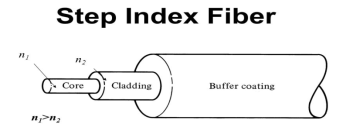
Figure: 19
A multimode step index fibre consists of a core of uniform refractive index surrounded by cladding of refractive index lower than that of the core. The refractive index abruptly changes at the core cladding boundary. The core is of large diameter. Light follows zigzag paths inside the fibre. Many such zigzag paths of propagation are permitted in Multi-Mode Fibre. The Numerical Aperture of a Multi-mode fibre is larger as the core diameter of the fibre is larger

Figure: 20
The refractive index of the optical fibre decreases as the radial distance from the fibre axis increases. GRIN fibre is one in which refractive index varies radially, decreasing continuously in a parabolic manner from the maximum value of n1, at the center of the core to a constant value of n2 at the core cladding interface.
In graded index fibre, light rays travel at different speeds in different parts of the fibre because the refractive index varies throughout the fibre. Near the outer edge, the refractive index is lower. As a result, rays near the outer edge travel faster than the rays at the center of the core. Because of this, rays arrive at the end of the fibre at approximately the same time. In effect light rays arrive at the end of the fibre are continuously refocused as they travel down the fibre. All rays take the same amount of time in traversing the fibre. This leads to small pulse dispersion.
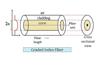
Figure: 21
For a parabolic index fibre, the pulse dispersion is reduced by a factor of about 200 in comparison to step index fibre. It is because of this reason that first and second generation optical communication systems used near parabolic index fibres.
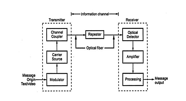
A fiber-optic link (or fiber channel) is a part of an optical fiber communications system which provides a data connection between two points (point-to-point connection). It essentially consists of a data transmitter, a transmission fiber (in some cases with built-in fiber amplifiers), and a receiver. Even for very long transmission distances, extremely high data rates of many Gbit/s or even several Tbit/s can be achieved.
The used components, which are mostly based on fiber optics, are explained in the following,

Figure22:Block Diagram of Optical Fiber CommunicationSystem
Generally message origin is from a transducer that converts a non-electrical message into an electrical signal. Common examples include microphones for converting sound waves into currents and video (TV) cameras for converting images into current. For data transfer between computers, the message is already in electrical form.
2. Modulator
The modulator has two main functions.
a) It converts the electrical message into the proper format.
b) It impresses this signal onto the wave generated by the carrier source.
c) Two distinct categories of modulation are used i.e. analog modulation and digital modulation.
3. Carrier source
Carrier source generates the wave on which the information is transmitted. This wave is called the carrier. For fiber optic system, a laser diode (LD) or a light emitting diode (LED) is used. They can be called as optic oscillators; they provide stable, single frequency waves with sufficient power for long distance propagation.
4. Channel coupler
Coupler feeds the power into the information channel. For an atmospheric optic system, the channel coupler is a lens used for collimating the light emitted by the source and directing this light towards the receiver. The coupler must efficiently transfer the modulated light beam from the source to the optic fiber. The channel coupler design is an important part of fiber system because of possibility of high losses.
5. Information channel
The information channel is the path between the transmitter and receiver. In fiber optic communications, a glass or plastic fiber is the channel. Desirable characteristics of the information channel include low attenuation and large light acceptance cone angle. Optical amplifiers boost the power levels of weak signals. Amplifiers are needed in very long links to provide sufficient power to the receiver. Repeaters can be used only for digital systems. They convert weak and distorted optical signals to electrical ones and then regenerate the original digital pulse trains for further transmission.
Another important property of the information channel is the propagation time of the waves travelling along it. A signal propagating along a fiber normally contains a range of optic frequencies and divides its power along several ray paths. This results in a distortion of the propagating signal. In a digital system, this distortion appears as a spreading and deforming of the pulses. The spreading is so great that adjacent pulses begin to overlap and become unrecognizable as separate bits of information.
6. Optical detector
The information being transmitted is detector. In the fiber system the optic wave is converted into an electric current by a photo detector. The current developed by the detector is proportional to the power in the incident optic wave. Detector output current contains the transmitted information. This detector output is then filtered to remove the constant bias and then amplified. The important properties of photo detectors are small size, economy, long life, low power consumption, high sensitivity to optic signals and fast response to quick variations in the optic power.
7. Signal processing
Signal processing includes filtering, amplification. Proper filtering maximizes the ratio of signal to unwanted power. For a digital system decision circuit is an additional block. The bit error rate (BER) should be very small for quality communications.
8. Message output
The electrical forms of the message emerging from the signal processor are transformed into a sound wave or visual image. Sometimes these signals are directly usable when computers or other machines are connected through a fiber system.
ADVANTAGES OF FIBRE OPTIC COMMUNICATION
The optical fibre communication has more advantages than convectional communication.
1. Enormous Bandwidth
2. Low Transmission Loss
The optical fibre communication has more advantages than convectional communication.
1. Enormous Bandwidth
2. Low Transmission Loss
3. Electric Isolation
4. Signal Security
5. Small Size and Less Weight
6. Immunity Cross Talk
1. Enormous bandwidth:- The information carrying capacity of a transmission system is directly proportional to the frequency of the transmitted signals. In the coaxial cable transmission the bandwidth range is up to around 500MHz only. Where as in optical fibre communication, the bandwidth range is large as 105 GHZ.
2. Low transmission loss:- The transmission loss is very low in optical fibres (i.e.KmdB/2.0) than compare with the conventional communication system. Hence for long distance communication fibres are preferred.
3. Electric isolation:- Since fibre optic materials are insulators, they do not exhibit earth and interface problems. Hence communicate through fibre even in electrically danger environment.
4. Signal security:- The transmitted signal through the fibre does not radiate, unlike the copper cables, a transmitted signal cannot be drawn from fibre without tampering it. Thus the optical fibre communication provides 100% signal security.
5. Small size and less weight:- The size of the fibre ranges from 10μm to 50μm, which is very small. The space occupied by the fibre cable is negligibly small compared to conventional electrical cables. Optical fibres are light in weight.
6. Immunity cross talk:- Since the optical fibres are dielectric wave guides, they are free from any electromagnetic interference and radio frequency interference. Since optical interference among different fibres is not possible, cross talk is negligible even many fibres are cabled together.
DISADVANTAGES OF OPTICAL FIBRE
The disadvantages of optical fibre include the following
BASICS OF CRYSTAL STRUCTURE
Crystallography is the experimental science of determining the arrangement of atoms in the crystalline solids. The properties of some materials are directly related to their crystal structures. So first of we will see what crystal structure is. Crystal structure can be defined as
Crystal structure
A crystal is a solid in which the constituent atoms, molecules or ions are packed in a regularly ordered, repeating pattern extending in three dimensions.
Based on the atomic arrangement in a substance, solids can be broadly classified as either crystalline solids or amorphous solids.
Crystalline Solids
In a crystalline solid, all the atoms are arranged in a periodic manner in all three dimensions. Crystalline solids need extreme temperatures to break the intermolecular forces. They have a definite heat of fusion and melting points because of the uniform arrangement of their components. The local environment is also uniform. However, when cut in any direction, the physical properties are different thus known as anisotropic. When rotated around the axis, the structure of crystals remains the same and that is termed as symmetrical arrangement of molecules, atoms or ions. The refractive index, mechanical strength, thermal conductivity and electrical conductivity of crystalline solids differ in different directions.
Amorphous solids
In a non-crystalline or amorphous solid the atomic arrangement is random or non-periodic in nature. The word amorphous is derived from the Greek word amorphous which means “shapeless”. This is the shapeless, disordered, and irregular arrangement of the constituent particles of a solid. Their inter-molecular forces are not the same nor are the distances between the particles. When cleaved, amorphous solids results in curved surfaces because of their irregular geometric shapes. Thermal conductivity, mechanical strength, electrical conductivity and refractive index are the same in all directions of amorphous solids. This explains where the name isotropic comes from. The solids do not have a sharp melting points or a definite heat of fusion. A wide range of temperature needs to be applied before they can melt because of the absence of an ordered array of components. Examples of amorphous solids include polymers, rubbers, plastics and glass.
Difference between Crystalline solids and amorphous solids
Crystalline solids | Amorphous solids |
|
|
2. They have long range order of regular pattern of arrangement of constituent particles. | 2. They have short range order of regular pattern of arrangement of constituent particles. |
3. They are true solids. | 3. They are pseudo solids or super cooled |
4. They have sharp melting points. | 4. They do not have sharp melting points. |
5. They are anisotropic in nature. | 5. They are isotropic in nature. |
6. They have definite heat of fusion. | 6. They do not have definite heat of fusion. |
Space Lattice or Crystal Lattice
In a solid crystalline material, the atoms or molecules are arranged regularly and periodically in all three dimensions. The atomic arrangement in a crystal is called crystal structure.
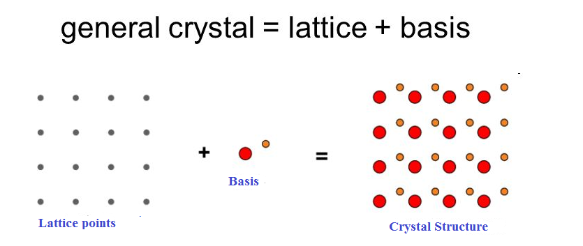
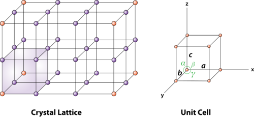
To explain crystal symmetries easily, it is convenient to represent an atom or a group of atoms that repeats in three dimensions in the crystal as a unit. If each such atom or unit of atoms in a crystal is replaced by a point in space, then the resultant points in space are called space lattice.
Each point in a space lattice is called a lattice point. Each atom or unit of atoms is called basis or pattern.
A space lattice or crystal lattice is defined as three dimensional infinite arrays of points in space in which every point has surroundings identical to that of every other point in the array.
Basis and Crystal Structure
The atomic arrangement in a crystal is called crystal structure. The crystal structure is formed by associating every lattice point with an atom or an assembly of atoms or molecules or ions, which are identical in composition, arrangement and orientation, called the basis. i.e. an atom, or a group of atoms or molecules identical in composition is called the basis or the pattern.
The basis provides the number of atoms per lattice point, their types, mutual orientations and distances of separation between the atoms.
If the basis is substituted for the lattice points, then the resulting structure is called crystal structure as shown in Figure.
lattice + basis = crystal structure.
The basis shown in Figure contains two different atoms. In copper and sodium crystals the basis is single atoms; In NaCl, the basis is diatomic and in CaF2 the basis is triatomic. A lattice is an imaginary assumption while the crystalstructure is a real concept.
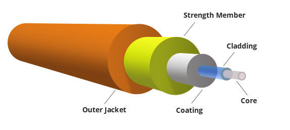
Figure 23: Lattice sites, Basis and crystal structure
Unit cell is small repeating entity of the atomic structure. It is the basic building block of the crystal structure. It defines the entire crystal structure with the atom positions within.
Unit cells for most of the crystals are parallelepipeds or cubes having three sets of parallel faces. A unit cell is the basic structural unit or building block of the crystal.
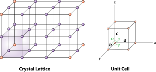
Figure 24: unit cell and unit cell parameter
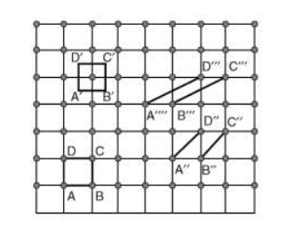
A unit cell is defined as the smallest parallelepiped volume in the crystal, which on repetition along the crystallographic axes gives the actual crystal structure or the smallest geometric figure, which on repetition in three-dimensional space, gives the actual crystal structure is called a unit cell.
Choice of a unit cell is not unique but it can be constructed in a number of ways as shown in figure. Following figure shows different ways of representing unit cells in a two-dimensional lattice. A unit cell can be represented as ABCD or A′B′C′D′ or A′′B′′C′′D′′, etc.
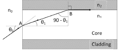
Figure 25: Construction of unit cell in different way
Unit cell parameters or lattice parameters
First we define crystallographic axes. These axes are obtained by the intersection of the three non-coplanar faces of the unit cell. The angles between these faces or crystallographic axes are known as interfacial or interaxial angles. The angles between the axes Y and Z is α, between Z and X is β and between X and Y is γ. The translational vectors or primitives a, b, c of a unit cell along X, Y, Z axes and interaxial angles α, β, γ are called Cell parameters. These cell parameters are shown in (Figure 24). The cell parameters determine the actual size and shape of the unit cell.
Primitive and non-primitive unit cells
The unit cell formed by primitives is called a simple or a primitive unit cell. A primitive unit cell contains only one lattice point. If a unit cell contains more than one lattice point, then it is called a non-primitive unit cell or a multiple unit cell. Most of the unit cells of various crystal lattices contain two or more lattice points and hence it is not necessary that unit cell should be a primitive unit cell.
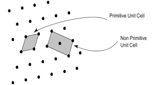
Figure 26: Primitive and non-primitive unit cells
When dealing with crystalline materials, it often becomes necessary to specify a particular point within a unit cell, a crystallographic direction, or some crystallographic plane of atoms.
Labelling conventions have been established in which three numbers or indices are used to designate point locations, directions, and planes. The basis for determining index values is the unit cell, with a right-handed coordinate system consisting of three (x, y, and z) axes situated at one of the corners and coinciding with the unit cell edges.
For some crystal systems—namely, hexagonal, rhombohedral, monoclinic, and triclinic-the three axes are not mutually perpendicular, as in the familiar Cartesian coordinate scheme. A crystallographic direction is defined as a line between two points, or a vector.
The following steps are utilized in the determination of the three directional indices:
1. A vector of convenient length is positioned such that it passes through the origin of the coordinate system. Any vector may be translated throughout the crystal lattice without alteration, if parallelism is maintained.
2. The length of the vector projection on each of the three axes is determined; these are measured in terms of the unit cell dimensions a, b, and c.
3. These three numbers are multiplied or divided by a common factor to reduce them to the smallest integer values.
4. The three indices, not separated by commas, are enclosed in square brackets, thus: [hkl]. The h, k, and l integers correspond to the reduced projections along the x, y, and z axes, respectively.
Crystal planes are defined as some imaginary planes inside a crystal in which large concentration of atoms are present. Inside the crystal, there exists certain direction along which large concentration of atoms exists. These directions are called crystal directions.
Miller Indices are a method of describing the orientation of a plane or set of planes within a lattice in relation to the unit cell. They were developed by William Hallowes Miller.
Crystal planes and directions can be represented by a set of three small integers called Miller indices [because Miller derived a method of representing crystal planes]. These integers are represented in general as h, k and l. If these integers are enclosed in round brackets as (hkl), then it represents a plane. On the other hand, if they are enclosed in square brackets as [hkl], then it represents crystal direction perpendicular to the above-said plane.
Procedure for drawing the given plane having Miller indices (hkl)
1.A unit cell is drawn with the given lattice parameters. After taking any convenient point as the origin O, the OX, OYand OZ crystallographic axes are to be marked. If lattice parameters are not given, then unit cubic cell of arbitrary lattice constant will be taken.
2.The reciprocals of the Miller indices 1/h, 1/k, 1/l are to be taken. These values provide the intercepts of the given plane on OX, OY and OZ axes, respectively.
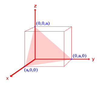
3.The intercepts are marked in the unit cell and the plane is drawn.
4. If the intercept is  on any axis, the plane drawn will be parallel to that axis.
Example:
Intercepts: a ,a , a
Fractional intercepts: 1 , 1 , 1
Miller Indices: (111)
|
Figure:27
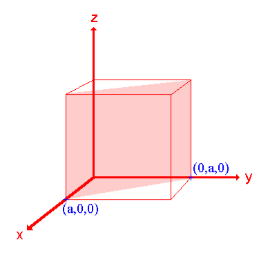
ii. The (110) surface
Intercepts: a ,a , ∞
Fractional intercepts: 1 , 1 , ∞
Miller Indices: (110)
|
|
Figure: 28
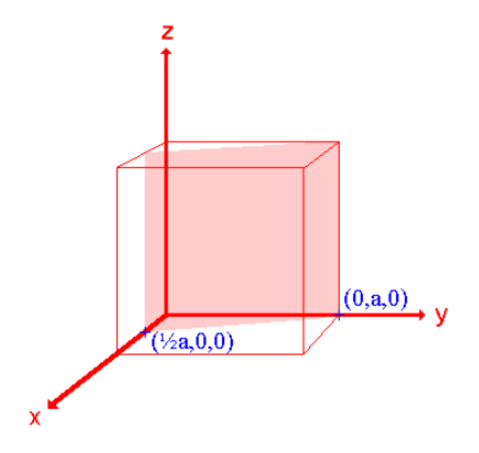
iii. The (210) surface
Intercepts: ½a ,a , 
Fractional intercepts: ½ , 1 , 
Miller Indices: (210)
|
|
Figure: 29
Table
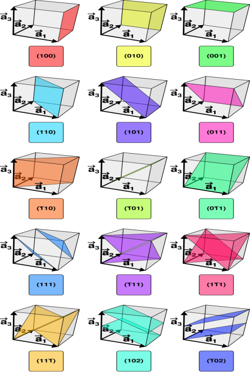
Figure:30
The fundamental property of a crystal is its triple periodicity and a Crystal may be generated by repeating a certain unit of pattern through the translations of a certain lattice called the direct lattice. The macroscopic geometric properties of a crystal are a direct consequence of the existence of this lattice on a microscopic scale. Let us for instance consider the natural faces of a crystal. These faces are parallel to sets of lattice planes. The lateral extension of these faces depends on the local physiochemical conditions during g-growth but not on the geometric properties of the lattice.
To describe the morphology of a crystal, the simplest way is to associate, with each set of lattice planes parallel to a natural face, a vector drawn from a given origin and normal to the corresponding lattice planes. To complete the description it suffices to give to each vector a length directly related to the spacing of the lattice planes. This polar diagram is the geometric basis for the reciprocal lattice.
On the other hand, the basic tool to study a crystal is the diffraction of a wave with a wavelength of the same order of magnitude as that of the lattice spacing. The nature of the diffraction pattern is governed by the triple periodicity and the positions of the diffraction spots depend directly on the properties of the lattice.
This operation transforms the direct space into an associated space, the reciprocal space, and the diffraction spots of a crystal are associated with the nodes of its reciprocal lattice. The reciprocal lattice is therefore an essential concept for the study of crystal lattices and their diffraction properties. This concept and the relation of the direct and reciprocal lattices through the Fourier transform was first introduced in crystallography by P. P. Ewald (.1921).
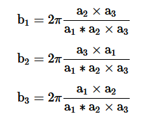
Every crystal structure has two lattices associated with it, the crystal lattice and the reciprocal lattice. A diffraction pattern of a crystal is the map of the reciprocal lattice of the crystal and a microscope structure is the map of the crystal structure. If a1, a2, a3 are the axis vectors of the real lattice, and b1, b2, b3are the axis vectors of the reciprocal lattice, they are related by the following equations:
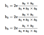
Using b1, b2, b3as a basis for a new lattice, then the vectors are given by
G=n1b1+n2b2+n3b3
Figure 31illustrates the 1-D, 2-D and 3-D real crystal lattices and its corresponding reciprocal lattices.
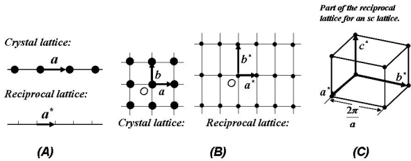
Figure 31: (a). Reciprocal lattice for a 1-D crystal lattice; (b).Reciprocal lattice for a 2-D crystal lattice; (c). Part of the reciprocal lattice for ansc lattice.
Based on the definition of the reciprocal lattice, the vectors of the reciprocal lattice can be related the crystal planes of the direct lattice:
(a) The vector Ghklis normal to the (hkl) crystal planes.
(b) The interplane distance dhklis related to the magnitude of Ghklby
dhkl=
The main features of the reciprocal lattice are:
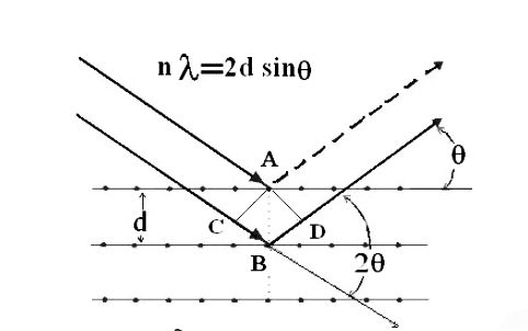
Consider a set of parallel planes called Bragg’s planes. Each atom is acting as a scattering center. The intensity of the reflected beam at certain angles will be maximum when the path difference between two reflected waves from two adjacent planes is an integral multiple of λ.
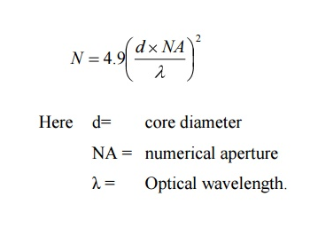
Figure 32
Let‘d’ be the distance between two adjacent planes, 'λ’ be the wavelength of the incident x-ray, ‘θ’ be the glancing angle.
The path difference between the rays reflected at A & B is given by
 =CB + BD= d sinθ + d sinθ = 2dsinθ
If the two consecutive planes scatter waves in phase with each other, then the path difference must be an integral multiple of wavelength.
 =nλ
=nλ
For the reflected light intensity to be maximum, the path difference
nλ= 2dsinθ
Where ‘n’ is the order of scattering.
This is called Bragg’s law
Therefore, Bragg’s law states that X-rays diffracted from different parallel planes of a crystal interfere constructively when the path difference is integral multiples of wavelength of X-rays.
From Bragg’s lawnλ = 2d sin θ, since maximum possible value for sin θ is 1,
nλ/2d≤ 1 or λ≤ 2d.
This sets the limitation on the wavelength, i.e. in order to get the diffraction pattern by a crystal, the wavelength of X-rays should not exceed twice the inter-planar spacing.
Importance of Bragg’s law:
1.Bragg’s law is the essential condition to be satisfied by crystal planes in order to get diffraction pattern from a crystal.
2.It is used to calculate inter-planar spacing. Knowing the values of inter-planar spacing, lattice parameters can be determined.
Fermions and bosons
There are only two types of fundamental particle known in the entire Universe: fermions and bosons. Every particle in addition to the normal propertieslike mass and electric charge has an intrinsic amount of angular momentum to it, known as spin.
Particles with spins that come in half-integer multiples (e.g., ±1/2, ±3/2, ±5/2, etc.) are known as fermions; particles with spins in integer multiples (e.g., 0, ±1, ±2, etc.) are bosons.
The first one is that only fermions have antiparticle counterparts. Quark's antiparticle is an antiquark. An electron's antiparticle is the positron (an anti-electron), while a neutrino has an antineutrino.
On the other hand, bosons are the antiparticles of other bosons, with many bosons being their own antiparticle. There is no such thing as an antiboson.
Bosons are particles with integer spin:
spin 0: 1Hand 4He in ground state, pion, Higgs boson
spin 1: 1Hand 4Hein first excited state, ρmeson, photon, W and Z bosons, gluons
spin 2: 16O in ground state, graviton.
Fermions are particles with half-integer spin:
Spin :3Hein ground state, proton, neutron, quark, electron, neutrino
Spin : 5Hein ground state,
  baryons (excitations of the proton and neutron)
Fermions obey the Pauli Exclusion Principle and therefore cannot co-exist in the same state at same location at the same time.Bosons don’t obey the Pauli Exclusion Principle.
Excitations will change the spin only by an integer amount. The basic building blocks of atoms are all fermions; composite particles (nuclei, atoms, molecules) made of an odd number of protons, neutrons and electrons are also fermions, whereas those made of an even number are bosons.
Distribution LawFor Bosons/Bose-Einstein Statistics
The basic postulates of BE statistics are:-
(i)The associated particles are identical and indistinguishable.
(ii)Each energy state can contain any number of particles.
(iii)Total energy and total number of particles of the entire system is constant
(iv)The particles have zero or integral spin,i.e. 0ℏ, 1 ℏ,5 ℏ,50 ℏetc, where ℏ is the unit of spin.
(v) The wavefunction of the system is symmetric under the positional exchange of any two particles. Examples: photon, phonon, all mesons (,,) etc., these are known as Bosons.
Symmetric and Anti-symmetric wave function
Suppose the allowed wave function for a n-particles system is ψ(1,2,3,.....,r,s,...n), where the integers within the argument of ψ represent the coordinates of the n-particles relative to some fixed origin. Now, if we interchange the positions of any two particles, say, r and s, the resulting wave function becomes ψ(1,2,3,....s,r,.....n). The wave function ψ is said to be symmetric when
ψ(1,2,3,.....,r,s,...n) = ψ(1,2,3,....s,r,.....n)
andAnti-symmetric when
ψ(1,2,3,.....,r,s,...n) = -ψ(1,2,3,....s,r,.....n)]
Bose-Einstein Distribution Law:
Let Ninumber of identical, indistinguishable, non-interactingparticles are to be distributed among giquantum states each having energy Ei. So, in the ithenergy level, there are (Ni+gi) total objects. Keeping the first quantum state fixed, the remaining (Ni+ gi-1)objects can permuted in (Ni+ gi-1)! possible ways. But since the particles and the quantum states are indistinguishable, we have to deduct Ni! ways and (gi–1)! ways from the all possible ways to get effective number of arrangements. Thus total number of possible ways of arrangement for theith state is
 ……….(1)
Hencethe total number of waysof the entire distribution of N particles in n number of energy levels of the system is
 ……….(2)
wheredenotes the product symbol.If we assume that Niand gi are very large, equation (2) reduces to
 ……….(3)
Taking natural logarithm of both the sides of equation (3) we get,
 ……….(4)
using Stirling approximation, Now, differentiating equation (4) to obtain the most probable distribution, we get,
Also we have other two conditions given by
 0 (conservation of total no of particles)………..(5)
 0 (conservation of total energy) ………..(6)
Multiplying equation (5) by (-α) and equation (6 )by (-β) and then adding with equation (4 )we get,
 ………..(7)
Since dNi’s are independent of one another, the above equation holds only if,
 ………..(8)
Now the Bose-Einstein distribution function is given by
 ………..(9)
which represents the probability of finding a boson with energy Ei.
Distribution LawFor Fermions/Fermi –Dirac Statistics
The basic postulates of FD statistics are:-
(i)Particles are identical and indistinguishable.
(ii)Total energy and total number of particles of the entire system is constant (iii)Particles have half-integral spin, i.e.etc, ,
,  ,
,  .
.
(iv)Particles obey Pauli’s exclusion principle, i.e. no two particles in a single system can have the same value for each of the four quantum numbers. In other words, a singleenergy state can contain at best a single particle with appropriate spin.
(v) The wave function of the system is anti-symmetric under the positional exchange of any two particles.
Examples: electron, proton, neutron, all hyperons (Λ,Σ,Ξ,Ω) etc., these are known as Fermions.
Fermi-Dirac Distribution Law:
Consider a system of N indistinguishable, non-interacting particles obeying Pauli’s exclusion principle. Let N1, N2, N3, ....Ni,....NnParticles in the system have energies E1, E2, E3, ....,Ei,...Enrespectively and let giis the number of degenerate quantum states in the energy level Ei. According to Pauli’s exclusion principle a single quantum state can be occupied by at best one particle. Since Niparticles are to be distributed among gidegenerate states (gi ≥Ni) having the same energy Ei, Nistates will be filled up and (gi -Ni) states will remain vacant. Now gi states can be arranged in gi! possible ways. But since the particles and the quantum states are indistinguishable, we have to deduct Ni! ways and (gi -Ni)! ways from the all possible ways to get effective number of arrangements. Thus total number of possible ways of arrangement for the ithstate is
 …………(1)
Hence the total number of ways for the entire distribution of N particles in n number of energy levels of the system is
 …………(2)
wheredenotes the product symbol.Now taking natural logarithm on both sides of equation (2) and applying Stirling approximation, we get,
 …………(3)
 …………(4)
Now, differentiating equation (4) to obtain the most probable distribution, we get,
 …………(5)
Considering the conservation of total energy and total number of particles, we can write
Also we have other two conditions given by
 0 (conservation of total no of particles)………..(6)
 0 (conservation of total energy) ………..(7)
Multiplying equation (6) by (-α) and equation (7)by (-β) and then adding with equation (5)we get,
 ………..(8)
Since dNi’s are independent of one another, the expression in thebracket of equation (8)is zero for each Ni. Thus
 ………..(9)
Hence the Fermi-Dirac distribution function is given by
 ………..(10)
which represents the probability of finding a fermion with energy Ei.
An isolated atom possesses discrete energies of different electrons. Suppose two isolated atoms are brought to very close, then the electrons in the orbits of two atoms interact with each other. So, that in this system, the energies of electrons will not be in the same level but changes and the energies will be slightly lower and larger than the original value. So, at the place of each energy level, a closely spaced two energy levels exists.
If ‘N’ number of atoms are brought together to form a solid and if these atoms’ electrons interact and give ‘N’ number of closely spaced energy levels in the place of discrete energy levels, it is known as bands of allowed energies. Between the bands of allowed energies, there are empty energy regions, called forbidden band of energies.
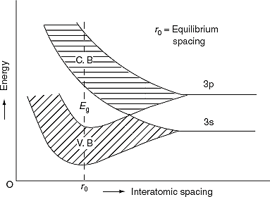
Figure 33
Kronig-Penney model shows the existence of band gap. Kronig-Penney model supports the existence of these bands of energies (allowed bands and forbidden bands).
The formation of energy bands has been explained taking Sodium (Na) metal as an example. When isolated sodium atoms are brought together to form a solid, then the energy levels of the valence electrons spread into bands. The 3S and 3P orbitals electrons energies are shown in Figure 33. These bands are seen to overlap strongly at the interatomic spacing of sodium.
We know that atoms have discrete energy levels. When a huge number of atoms are combined to form a solid, these discrete energy levels are replaced by discrete ranges of energy or called as energy bands.
In energy bands there are so many individual allowed energy values or you can saythat the energy bands the energy distribution is continuous. Thisis shown in the following figure
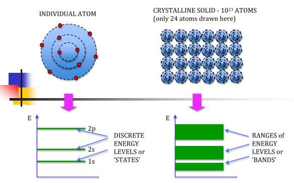
Figure 34
In between energy bands are ranges of energy which are entirely impossible known as band gaps
Different substances have different band structures which explain the characteristics of that substance in terms of electrical conduction.
Bands are formed by the closely spaced orbitals. There are three types of bands:
1. Valance Bands:Valence band it is a group of orbitals which contain electrons in the shell. Or we can sayIt is also defined as the energy band that comprises of valence electrons present in the outermost shell of an atomic structure.
These valence electrons, when provided with sufficient energy, get changed into free electrons and moves to conduction band thereby causing conductivity. It is at a lower energy level than the conduction band in the energy level diagram.
2. Conduction Band: Conduction band is a group of empty orbitals of the shells that do not contain any electron due to their configuration making the orbitals of higher energy levels.
When the electrons pass from valance band to the conduction band these solids conduct electricity with flow of charges in the form of electrons.
3. Forbidden Energy Band: These two bands are separated by a certain amount of energy known as the forbidden energy gap. In this band not a single electron is available. It diagram it is named as Band Gap.
Let us distinguish between conductor, semiconductors and insulator on the basis of these bands.
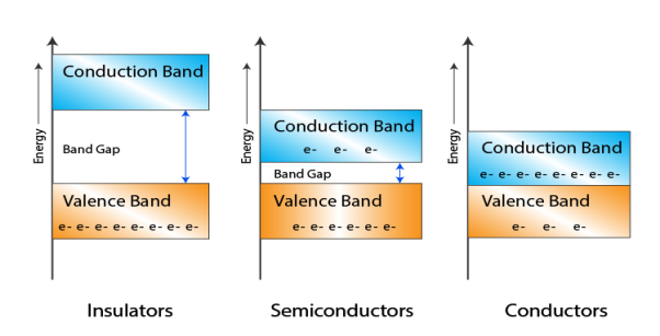 Figure 35
Consider an isolated silicon atom; its energy levels are quantized. When two identical atoms are brought closer together, the quantized energy levels hybridize and split into two different levels because of the mutual interaction of the two atoms. More generally, when N atoms are moved closer, until they reach the equilibrium inter-atomic distance d, the energy levels split into N levels. These N levels are very close to each other if N is large (which is the case in a crystal) so that they eventually form a continuous energy band.
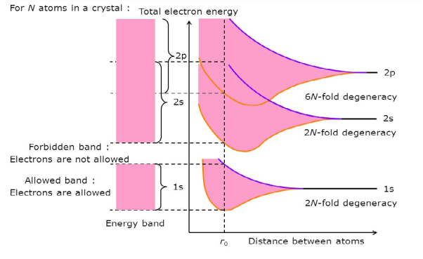
Figure 36: Formation of Energy band as a function of interatomic distance (distance between atoms)
