Unit – 1
Introduction
- It deals with binary numbers & variables.
- Therefore, also known as Binary Algebra or logical Algebra.
- A mathematician named as George Boole had developed this algebra in 1854.
- The variables that are used in this algebra are known as Boolean variables.
- Considering the range of voltages as logic ‘High’ is represented with ‘1’ and logic ‘Low’ is represented with ‘0’.
Using a transistor as a switch is the simplest application of the device. A transistor can be extensively used for switching operation either for opening or closing of a circuit. Meanwhile, the basic concept behind the operation of a transistor as a switch relies on its mode of operation. Generally, the low voltage DC is turned on or off by transistors in this mode.
Both PNP and NPN transistors can be utilized as switches. A basic terminal transistor can be handled differently from a signal amplifier by biasing both NPN and PNP bipolar transistors by an “ON / OFF” static switch. One of the main uses of the transistor to transform a DC signal “On” or “OFF” is solid-state switches.
Some devices, including LEDs, only require several milliamperes of DC voltages at the logical level and can be directly controlled via the logical gate output. High-power devices such as generators, solenoids or lamps usually need more power to use transistor switches than the usual logic gate.
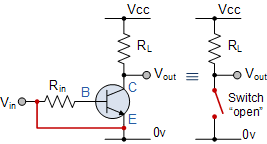
Fig.1: Transistor as a switch
Cut-Off Region
The “cut-off” area is at the bottom of the curves, the blue, shaded area and the yellow zone on the left is the transistor “saturation” region.
The transistor’s operating specifications include the base current (IB), the collector current (IC) and the emitter-collector voltage (VCE).
Characteristics of Cut-off Region
- The transistor is used as an “open switch”
- The bases and input are grounded (0v)
- The base emission voltage is VBE > 0.7 V
- The basic emitter is reversed
- The full-OFF (cut-off area) transistor (“Collector Flow = 0”) • VOUT = VCC = “1′′”
- No collector current flows (IC = 0)
Instead, we can describe the “cut-off region” or “OFF mode,” both in reverse bias, with Vb < 0.7 V and IC = 0, when using a bipolar transistor as a switch.
CMOS inverter
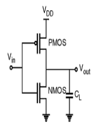
Fig 2: CMOS inverter
- It consists of PMOS and NMOS FET.
- The input A serves as the gate voltage for both transistors.
- The NMOS transistor has an input from Vss (ground) and PMOS transistor has an input from Vdd. The terminal Y is output.
- When a high voltage (~ Vdd) is given at input terminal (A) of the inverter, the PMOS becomes open circuit and NMOS switched OFF so the output will be pulled down to Vss.
- The truth table of inverter is:
A | Y = A’ |
0 | 1 |
1 | 0 |
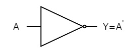
Fig. 3: NOT gate
CMOS Two input NOR Gate
The circuit consists of a parallel-connected n-net and a series-connected complementary p-net. The input voltages VX and VY are applied to the gates of one nMOS and one pMOS transistor.
When either one or both inputs are 1, then p-net is 0 (cut—off).
If both input voltages are 0, then the p-net conducts between the output node and the supply voltage
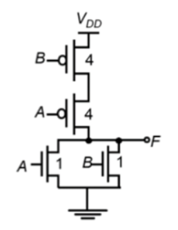
Fig 4: Layout of CMOS NOR Gate
CMOS Two-input NAND Gate
Here, the n – net consists of two series connected nMOS transistor conducts between the output node and the ground, if both input voltages are 1. Both of the parallelly connected pMOS transistor in p-net will be off.
For all other input combination, either one or both of the pMOS transistor will be turn ON, while p – net is cut off, thus, conducts between the output node and the power supply voltage.
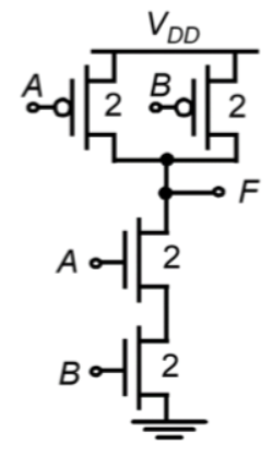
Fig 5: Layout of CMOS NOR Gate
- A Sequential circuit consists of inputs variable (X), logic gates and output variable (Z).
- Combinational circuit generates an output on the basis of input variable only but Sequential circuit produces an output based on current input and previous output variables.
- This means that it includes memory elements which are capable of storing binary information.
- This binary information is nothing but the state of the sequential circuit at any given time. A latch capable of storing one bit information.

Fig. 6 Combinational circuit
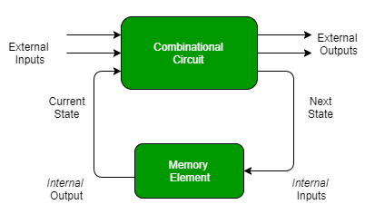
Fig. 7 Sequential circuit
There are two types of input to the combinational logic in fig 2:
- External inputs which are not controlled by the circuit.
- Internal inputs which are function of previous output states.
Secondary inputs are state variables that are produced by the storage elements whereas secondary outputs are excitations for those storage elements.
Types of Sequential Circuits –
There are two types of sequential circuit:
Asynchronous sequential circuit –
- They do not use a clock signal but instead uses the pulses as inputs.
- These circuits are faster because there is clock pulse and can change their state immediately when there is a change in the input signal.
- It is used when speed of operation is important and is independent of internal clock pulse.

Fig. 8 Asynchronous Sequential circuit
But they are more difficult to design and their output is also uncertain.
Synchronous sequential circuit –
- These circuit uses clock signal and level inputs.
- The output pulse is received in the same duration as the clock pulse for the clocked sequential circuits.
- They wait for the next clock pulse to arrive to perform the next operation, these circuits are bit slower as compared to asynchronous circuits.
- Level output changes state at the start of an input pulse and remains in that state until the next input or clock pulse arrives.
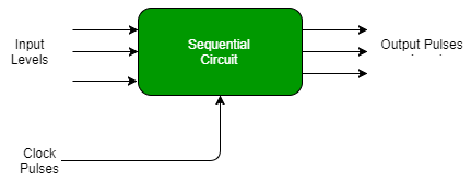
Fig. 9 Synchronous Sequential circuit
- It is used in synchronous counters, flip flops, and in MOORE-MEALY machines.
- It is also used to design Counters, Registers, RAM, etc
Key takeaway
Asynchronous sequential circuit –
- They do not use a clock signal but instead uses the pulses as inputs.
- These circuits are faster because there is clock pulse and can change their state immediately when there is a change in the input signal.
Synchronous sequential circuit –
- These circuit uses clock signal and level inputs.
- The output pulse is received in the same duration as the clock pulse for the clocked sequential circuits.
Clocked S-R flipflop
SR Latch is a circuit which has:
(i) 2 cross-coupled NOR gate or NAND gate.
(ii) 2 input S for SET and R for RESET.
(iii) 2 output Q and Q’.
Q | Q’ | STATE |
1 | 0 | Set |
0 | 1 | Reset |
Under normal conditions, both the input remains 0.
RS Latch with NAND gates:
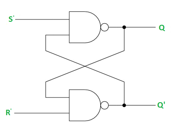
Case-1: When S’=R’=1 or S=R=0 then
If Q = 1, Q = R’ = 1.
If Q = 0, Q = 0 and R’ = 1 respectively.
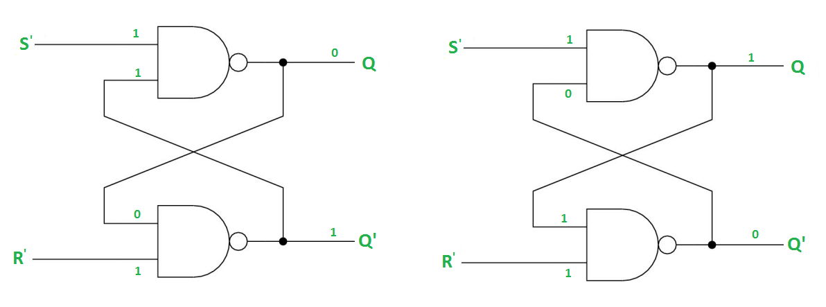
Case-2: S’=0, R’=1 (S=1, R=0)
As S’=0, Q = 1(SET state).
In 2nd NAND gate, as Q = R’ = 1, Q’=0.
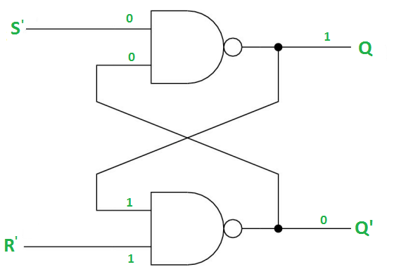
Case-3: S’= 1, R’= 0 (S=0, R=1)
As R’=0, Q’ = 1.
In 1st NAND gate, as Q =S’ = 1, Q=0 (RESET state).
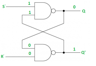
Case-4: S’= R’= 0 (S=R=1)
When S=R=1, both Q = Q’ = 1 which is not allowed.
So, this input condition is prohibited.
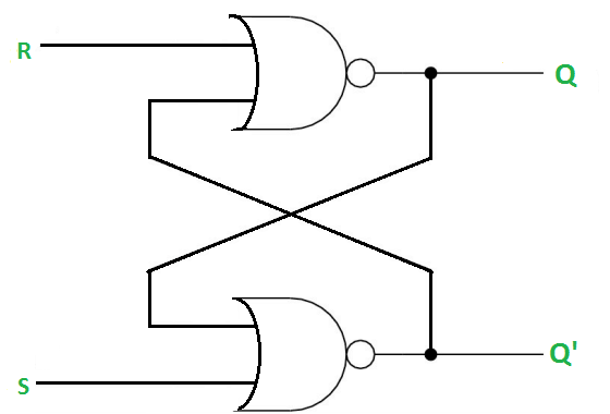
The SR Latch using NOR gate is:
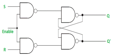
Gated SR Latch –
It is a latch which enable input that works when enable = 1 and retain the previous state when enable = 0.
Gated D Latch –
It is similar to SR latch with little modifications. Here, the inputs are complements of one another. The design of D latch with Enable signal is given below:

The truth table is shown below:
ENABLE | D | Q(N) | Q(N+1) | STATE |
1 | 0 | x | 0 | RESET |
1 | 1 | x | 1 | SET |
0 | x | x | Q(n) | No Change |
As the output is same as input, it is also known as Transparent Latch.
The characteristic equation for D latch with enable input is given as:
Q(n+1) = EN.D + EN'.Q(n)
Shift Registers
- Flip flops are used to store one bit of binary data (1or 0).
- If we need to store multiple bits of data, we use multiple flip flops.
- N flip flops are connected to store n bits of data.
- A Register is a device which stores such information. It is a group of flip flops connected in series which is used to store multiple bits of data.
- The information stored in these registers can be transferred with the help of shift registers.
- This register is a group of flip flops used to store multiple bits of data.
- The bits stored in these registers can be moved in/out of the registers by applying clock pulses.
- The registers which shift the bits towards left are called “Shift left registers”.
The registers which shift the bits towards right are called “Shift right registers”.
Shift registers are of 4 types and they are:
- Serial In Serial Out register
- Serial In parallel Out register
- Parallel In Serial Out register
- Parallel In parallel Out register
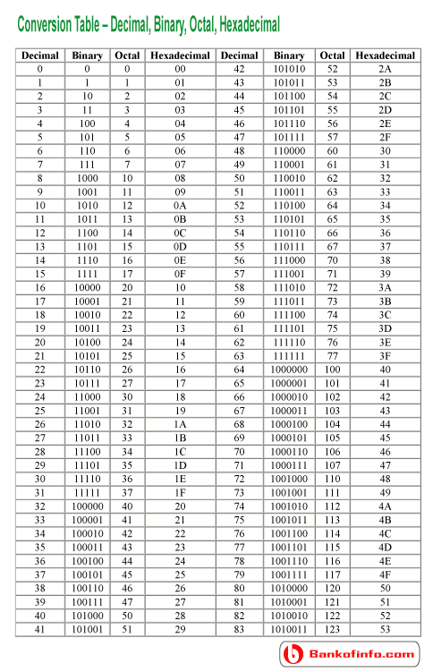
A digital system understands positional number system where there are few symbols called digits and these symbols represents different values depending on their position in the number.
A value of the digit is determined by using
- The digit
- Its position
- The base of the number system
Decimal Number System
- It’s the system that we use in our daily life. It has a base 10 and uses 10 digits from 0 to 9.
- Here, the successive positions towards the left of the decimal point represent units, tens, hundreds, thousands and so on.
- Each and every position represents a specific power of the base (10). For example, the decimal number 4321 consists of the digit 1 in the unit’s position, 2 in the tens position, 3 in the hundreds position, and 4 in the thousands position, and its value can be written as
(1×1000) + (2×100) + (3×10) + (4×l)
(1×10³) + (2×10²) + (3×101) + (4×l00)
1000 + 200 + 30 + 1
1234
- As a computer programmer, we should understand the following number systems used in computers.
S.N. | Number System & Description |
1 | Binary Number System Base 2. Digits used: 0 and 1 |
2 | Octal Number System Base 8. Digits used: 0 to 7 |
3 | Hexa Decimal Number System Base 16. Digits used: 0 to 9, Letters used: A- F |
Binary Number System
- It uses two digits 0 and 1.
- It is also called as base 2 number system.
- Here, each position in any binary number represents a power of the base (2). Example: 23
- The last position represents a y power of the base (2). Example: 2y where y represents the last position.
Example
Binary Number: 101112
Calculating the Decimal Equivalent of binary number −
Step | Binary Number | Decimal Number |
Step 1 | 101012 | ((1 × 24) + (0 × 23) + (1 × 22) + (1 × 21) + (1 × 20))10 |
Step 2 | 101012 | (16 + 0 + 4 + 2 + 1)10 |
Step 3 | 101012 | 2310 |
Note: 101112 is normally written as 10111.
Octal Number System
- It consists of eight digits 0, 1,2,3,4,5,6,7.
- It is also named as base 8 number system.
- Here each position represents a power of the base (8). Example: 82
- The last position represents a y power of the base (8). Example: 8y where y represents the last position.
Example
Octal Number − 125758
Calculating Decimal Equivalent −
Step | Octal Number | Decimal Number |
Step 1 | 125758 | ((1 × 84) + (2 × 83) + (5 × 82) + (7 × 81) + (5 × 80))10 |
Step 2 | 125758 | (4096 + 1024 + 320 + 56 + 5)10 |
Step 3 | 125758 | 550010 |
Note: 125758 is normally written as 12575 in octal.
Hexadecimal Number System
- It uses 10 digits starting from 0,1,2,3,4,5,6,7,8,9 and 6 letters A, B, C, D, E, F.
- These letters represent numbers as A = 10, B = 11, C = 12, D = 13, E = 14, F = 15.
- It is also known as base 16 number system.
- Here each position represents a power of the base (16). Example 161.
- The last position represents a y power of the base (16). Example: 16y where y represents the last position.
Example −
Hexadecimal Number: 19FDA16
Calculating Decimal Equivalent −
Step | Hexadecimal Number | Decimal Number |
Step 1 | 19FDA16 | ((1 × 164) + (9 × 163) + (F × 162) + (D × 161) + (A × 160))10 |
Step 2 | 19FDA16 | ((1 × 164) + (9 × 163) + (15 × 162) + (13 × 161) + (10 × 160))10 |
Step 3 | 19FDA16 | (65536 + 36864 + 3840 + 208 + 10)10 |
Step 4 | 19FDA16 | 10645810 |
Note − 19FDA16 is normally written as 19FDA in hexa decimal.
Conversions:
There are many techniques which are used to convert numbers from one base to another. These are as follows −
- Decimal to any other Base System
- Any Base System to Decimal
- Any Base System to Non-Decimal
- Binary to Octal
- Octal to Binary
- Binary to Hexadecimal
- Hexadecimal to Binary
Decimal to Any Base System
It includes the following steps:
- Firstly, divide the decimal number which is to be converted by the value of its new base.
- Then, after getting the remainder from the above step make it the rightmost digit (least significant digit) i.e., LSD of new base number.
- Further divide the quotient by the new base.
- Then record the remainder from the above step as the next digit (towards the left) of the new base number.
- Repeat these steps and get remainders from right to left till the quotient becomes zero.
- The last remainder obtained will be the Most Significant Digit (MSD) of the new base number.
For example −
Decimal Number: 2710
Calculating Binary Equivalent −
Step | Operation | Result | Remainder |
Step 1 | 27 / 2 | 13 | 1 |
Step 2 | 13 / 2 | 6 | 1 |
Step 3 | 6 / 2 | 3 | 0 |
Step 4 | 3 / 2 | 1 | 1 |
Step 5 | 1 / 2 | 0 | 1 |
Hence, the remainders are arranged in the reverse order and we get:
Decimal Number − 2710 = Binary Number − 110112.
Any Base System to Decimal System
- Here, the column (positional) value of each digit (this depends on the position of the digit and the base of the number system) is multiplied with the obtained column values of the digits in the corresponding columns.
- The sum the products is then calculated which gives the total equivalent value in decimal.
For example:
Binary Number − 111102
Calculating Decimal Equivalent −
Step | Binary Number | Decimal Number |
Step 1 | 111102 | ((1 × 24) + (1 × 23) + (1 × 22) + (1 × 21) + (0 × 20))10 |
Step 2 | 111102 | (16 + 8 + 4 + 2 + 0)10 |
Step 3 | 111102 | 3010 |
Binary Number − 111102 = Decimal Number − 3010
Any Base System to Non-Decimal System
- The original number is converted to its equivalent decimal number (base 10).
- Then the decimal number so obtained is further converted to the new base number.
Example
Octal Number − 268
Calculating its Binary Equivalent −
Step 1 – Converting octal to Decimal
Step | Octal Number | Decimal Number |
Step 1 | 268 | ((2 × 81) + (6 × 80))10 |
Step 2 | 268 | (16 + 6 )10 |
Step 3 | 268 | 2210 |
Octal Number − 268 = Decimal Number − 2210
Step 2 − Converting Decimal to Binary
Step | Operation | Result | Remainder |
Step 1 | 22 / 2 | 11 | 0 |
Step 2 | 11 / 2 | 5 | 1 |
Step 3 | 5 / 2 | 2 | 1 |
Step 4 | 2 / 2 | 1 | 0 |
Step 5 | 1 / 2 | 0 | 1 |
Decimal Number − 2210 = Binary Number − 101102
Octal Number − 268 = Binary Number − 101102
Binary to Octal
- Dividing the binary digits into groups of three starting from right to left.
- Converting each group of three binary digits into one octal digit.
For example:
Binary Number − 101012
Its Octal Equivalent −
Step | Binary Number | Octal Number |
Step 1 | 101012 | 010 101 |
Step 2 | 101012 | 28 58 |
Step 3 | 101012 | 258 |
Binary Number − 101012 = Octal Number − 258
Octal to Binary
- Converting each octal digit to a 3-digit binary number and they can be treated as decimal number for this conversion.
- Then combining all the resulting binary groups into a single binary number.
For example:
Octal Number − 258
Its Binary Equivalent −
Step | Octal Number | Binary Number |
Step 1 | 258 | 210 510 |
Step 2 | 258 | 0102 1012 |
Step 3 | 258 | 0101012 |
Octal Number − 258 = Binary Number − 101012
Binary to Hexadecimal
- Dividing the binary digits into groups of four (starting from right to left).
- Then converting each group of four binary digits into one hexadecimal number.
For example:
Binary Number − 101012
Its hexadecimal Equivalent −
Step | Binary Number | Hexadecimal Number |
Step 1 | 101012 | 0001 0101 |
Step 2 | 101012 | 110 510 |
Step 3 | 101012 | 1516 |
Binary Number − 101012 = Hexadecimal Number − 1516
Hexadecimal to Binary
- Converting each hexadecimal digit to a 4-digit binary number and they can be treated as decimal number.
- Combining all the resulting binary groups into a single binary number.
For example:
Hexadecimal Number − 1516
Its Binary Equivalent −
Step | Hexadecimal Number | Binary Number |
Step 1 | 1516 | 110 510 |
Step 2 | 1516 | 00012 01012 |
Step 3 | 1516 | 000101012 |
Hexadecimal Number − 1516 = Binary Number − 101012
Key takeaway
- In coding, when alpha-numeric characters or words are represented by a specific group of symbols, it is said that it is being coded.
- The group of symbols is known as a code.
- The digital data can be represented, stored and transmitted as group of binary bits.
- This group is called as binary code.
- It is represented by the number as well as alphanumeric character.
Advantages of Binary Code
- They are used in computer applications.
- They are suitable for digital communications.
- They make the analysis and designing of digital circuits easy.
- Implementation becomes very easy since only 0 & 1 are being used.
Classification of binary codes
The codes are broadly classified as:
- Weighted Codes
- Non-Weighted Codes
- Binary Coded Decimal Code
- Alphanumeric Codes
- Error Detecting Codes
- Error Correcting Codes
- It is the non-weighted code and is not an arithmetic code.
- This means that there are no specific weights assigned to the bit position.
- Here only one bit will change every time the decimal number is incremented.
- The gray code is also known as a unit distance code as only one-bit changes at a time.
- The gray code is a type of cyclic code.
- It cannot be used for all arithmetic operation.
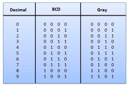
Fig.10: Gray codes
Application of Gray code
- They are used in the shaft position encoders.
- This encoder produces a code word which represents the angular position of the shaft.
When bits are being transmitted over the computer network, they get corrupted due to interference and network problems.
These corrupted bits leads to spurious data that is being received by the receiver and are called errors.
Hence the Error-correcting codes (ECC) are a sequence of numbers which are generated by specific algorithms for detecting and removing errors in data that can be transmitted over various noisy channels.
They ascertain the exact number of bits that has been corrupted and the also their location in algorithm.
ECCs are of two types −
- Block codes − The message is divided into fixed-sized blocks of bits which are added for error detection or correction.
- Convolutional codes − The message consists of data streams of arbitrary length and parity symbols are being generated by sliding the application of a Boolean function to the data stream.
Hamming Code
It is a block code which is capable of detecting up to two simultaneous bit errors and correcting single-bit errors.
It was developed by R.W. Hamming for error correction.
In this method, the source encodes the message by inserting some redundant bits within the message.
These bits are extra bits that can be generated and inserted at specific positions in the message to enable error detection and correction.
When the destination receives this message recalculations are done to detect errors and finding the bit position that has error.
Encoding a message by Hamming Code
It requires the following steps −
- Calculating the number of redundant bits.
- Positioning them.
- Then calculating the values of each of the redundant bits.
- Once these bits are embedded in the message, this is sent to the user.
Step 1 − Calculating the number of redundant bits.
- The message contains m number of data bits, r number of redundant bits are added to it so that m𝑟 is will indicate at least (m + r+ 1) different states.
- Here, (m + r) indicates location of an error in each of (𝑚 + 𝑟) bit positions and one additional state indicates no error.
- Since, r bits can indicate 2r𝑟 states then 2r𝑟 must be equal to (m + r + 1).
- Thus the following equation should hold 2r ≥ m+r+1
Step 2- Positioning them.
- The r redundant bits placed at various bit positions of powers of 2, i.e. 1, 2, 4, 8, 16 etc.
- They are referred as r1 (at position 1), r2 (at position 2), r3 (at position 4), r4 (at position 8) and so on.
Step 3 − Calculating the values of each of the redundant bits
The redundant bits are parity bits.
A parity bit is an extra bit that makes the number of 1s either even or odd.
There are two types of parity bits −
- Even Parity − where the total number of bits in the message is even.
- Odd Parity − where the total number of bits in the message is odd.
Each redundant bit, r, is based upon its bit position.
It covers all bit positions whose binary representation includes a 1 in the ith position except the position of ri. Thus −
- r1 is the parity bit for all positions representing 1 in the least significant position excluding 1 (3, 5, 7, 9, 11 and so on)
- r2 is the parity bit for all positions representing 1 in the position 2 from right except 2 (3, 6, 7, 10, 11 and so on)
- r3 is the parity bit for all positions representing 1 in the position 3 from right except 4 (5-7, 12-15, 20-23 and so on)
Decoding a message in Hamming Code
Once the receiver gets an incoming message, recalculations are done to detect errors and correct them. The steps for recalculation are −
- Calculation of the number of redundant bits.
- Positioning the redundant bits.
- Parity checking.
- Error detection and correction
Step 1 − Calculation of the number of redundant bits
Using the same method as in encoding, the number of redundant bits are ascertained.
2r ≥ m + r + 1
Where m is and r have their usual meaning.
Step 2 − Positioning the redundant bits
The r redundant bits placed at bit positions of powers of 2.
Step 3 − Parity checking
They are calculated on the basis of the data bits and the redundant bits using the same rule as during generation. Thus
c1 = parity(1, 3, 5, 7, 9, 11 and so on)
c2 = parity(2, 3, 6, 7, 10, 11 and so on)
c3 = parity(4 to7, 12-15, 20 to 23 and so on)
Step 4 − Error detection and correction
The decimal equivalent of the parity bits is calculated. If it is a 0, then there is no error. Else, the decimal value gives the bit position which has error.
For example, if c1c2c3c4 = 1000, it implies that the data bit at position 8, decimal equivalent of 1000, has error.
The bit is flipped to get the correct message.
A register is a set of flip-flops with combinational logic to implement state transitions that allow information to be stored and retrieved from them. In the simplest form, a flip-flop is a one-bit register.
- In coding, when alpha-numeric characters or words are represented by a specific group of symbols, it is said that it is being coded.
- The group of symbols is known as a code.
- The digital data can be represented, stored and transmitted as group of binary bits.
- This group is called as binary code.
- It is represented by the number as well as alphanumeric character.
Advantages of Binary Code
- They are used in computer applications.
- They are suitable for digital communications.
- They make the analysis and designing of digital circuits easy.
- Implementation becomes very easy since only 0 & 1 are being used.
Classification of binary codes
The codes are broadly classified as:
- Weighted Codes
- Non-Weighted Codes
- Binary Coded Decimal Code
- Alphanumeric Codes
- Error Detecting Codes
- Error Correcting Codes
The basic gates are namely AND gate, OR gate & NOT gate.
AND gate
It is a digital circuit that consists of two or more inputs and a single output which is the logical AND of all those inputs. It is represented with the symbol ‘.’.
The following is the truth table of 2-input AND gate.
A | B | Y = A. B |
0 | 0 | 0 |
0 | 1 | 0 |
1 | 0 | 0 |
1 | 1 | 1 |
Here A, B are the inputs and Y is the output of two input AND gate.
If both inputs are ‘1’, then only the output, Y is ‘1’. For remaining combinations of inputs, the output, Y is ‘0’.
The figure below shows the symbol of an AND gate, which is having two inputs A, B and one output, Y.

Fig. 11: AND gate
OR gate
It is a digital circuit which has two or more inputs and a single output which is the logical OR of all those inputs. It is represented with the symbol ‘+’.
The truth table of 2-input OR gate is:
A | B | Y = A + B |
0 | 0 | 0 |
0 | 1 | 1 |
1 | 0 | 1 |
1 | 1 | 1 |
Here A, B are the inputs and Y is the output of two input OR gate.
When both inputs are ‘0’, then only the output, Y is ‘0’. For remaining combinations of inputs, the output, Y is ‘1’.
The figure below shows the symbol of an OR gate, which is having two inputs A, B and one output, Y.

Fig. 12: OR gate
NOT gate
It is a digital circuit that has one input and one output. Here the output is the logical inversion of input. Hence, it is also called as an inverter.
The truth table of NOT gate is:
A | Y = A’ |
0 | 1 |
1 | 0 |
Here A and Y are the corresponding input and output of NOT gate. When A is ‘0’, then, Y is ‘1’. Similarly, when, A is ‘1’, then, Y is ‘0’.
The figure below shows the symbol of NOT gate, which has one input, A and one output, Y.

Fig. 13: NOT gate
- It deals with binary numbers & variables.
- Therefore, also known as Binary Algebra or logical Algebra.
- A mathematician named as George Boole had developed this algebra in 1854.
- The variables that are used in this algebra are known as Boolean variables.
- Considering the range of voltages as logic ‘High’ is represented with ‘1’ and logic ‘Low’ is represented with ‘0’.
Postulates and Basic Laws of Boolean Algebra
Here, the Boolean postulates and basic laws that are used are given underneath.
Boolean Postulates
- Considering the binary numbers 0 and 1, boolean variable (x) and its complement (x’).
- They known as literal.
- The possible logical OR operations are:
x + 0 = x
x + 1 = 1
x + x = x
x + x’ = 1
- Similarly, the possible logical AND operations are:
x.1 = x
x.0 = 0
x.x = x
x.x’ = 0
- These are the simple Boolean postulates and verification can be done by substituting the Boolean variable with ‘0’ or ‘1’.
Basic Laws of Boolean Algebra
The three basic laws of Boolean Algebra are:
- Commutative law
- Associative law
- Distributive law
Commutative Law
- The logical operation carried between two Boolean variables when gives the same result irrespective of the order the two variables, then that operation is said to be Commutative. The logical OR & logical AND operations between x & y are shown below
x + y = y + x
x.y = y.x
- The symbol ‘+’ and ‘.’ indicates logical OR operation and logical AND operation.
- Commutative law holds good for logical OR & logical AND operations.
Associative Law
- If a logical OR operation of any two Boolean variables is performed first and then the same operation is performed with the remaining variable providing the same result, then that operation is said to be Associative. The logical OR & logical AND operations of x, y & z are:
x + (y + z) = (x + y) + z
x.(y.z) = (x.y).z
- Associative law holds good for logical OR & logical AND operations.
Distributive Law
- If a logical OR operation of any two Boolean variables is performed first and then AND operation is performed with the remaining variable, then that logical operation is said to be Distributive. The distribution of logical OR & logical AND operations between variables x, y & z are :
x.(y + z) = x.y + x.z
x + (y.z) = (x + y).(x + z)
- Distributive law holds good for logical OR and logical AND operations.
- These are the Basic laws of Boolean algebra and we can verify them by substituting the Boolean variables with ‘0’ or ‘1’.
Theorems of Boolean Algebra
The following theorems are used in Boolean algebra.
- Duality theorem
- De Morgan’s theorem
Duality Theorem
- It states that “The dual of the Boolean function is obtained by interchanging the logical AND operator with logical OR operator and zeros with ones”.
- For every Boolean function, there is a Dual function.
- Let us make the Boolean equations (relations) of Boolean postulates and basic laws into two groups. The following table shows these two groups.
Group1 | Group2 |
x + 0 = x | x.1 = x |
x + 1 = 1 | x.0 = 0 |
x + x = x | x.x = x |
x + x’ = 1 | x.x’ = 0 |
x + y = y + x | x.y = y.x |
x + (y + z) = (x + y) + z | x.(y.z) = (x.y).z |
x.(y + z) = x.y + x.z | x + (y.z) = (x + y).(x + z) |
- Every row comprise of two Boolean equations and they are dual to one other.
- We can also verify the Boolean equations of Group1 and 2 by using duality theorem.
De Morgan’s Theorem
- It is useful in finding the complement of Boolean function.
- It states that “The complement of logical OR of at least two Boolean variables is equal to the logical AND of each complemented variable”.
- It can be represented using 2 Boolean variables x and y as
(x + y)’ = x’.y’
- The dual of the above Boolean function is
(x.y)’ = x’ + y’
- Therefore, the complement of logical AND of the two Boolean variables is equivalent to the logical OR of each complemented variable.
- Similarly, DeMorgan’s theorem can be applied for more than 2 Boolean variables also.
Numerical
- Simplify the Boolean function,
f = p’qr + pq’r + pqr’ + pqr
Method 1
Given
f = p’qr + pq’r + pqr’ +pqr.
In first and second term r is common and in third and fourth terms pq is common.
So, taking out the common terms by using Distributive law we get,
⇒ f = (p’q + pq’)r + pq(r’ + r)
The terms present in first parenthesis can be simplified by using Ex-OR operation.
The terms present in second parenthesis is equal to ‘1’ using Boolean postulate we get
⇒ f = (p ⊕q)r + pq(1)
The first term can’t be simplified further.
But, the second term is equal to pq using Boolean postulate.
⇒ f = (p ⊕q)r + pq
Therefore, the simplified Boolean function is f = (p⊕q)r + pq
Method 2
Given f = p’qr + pq’r + pqr’ + pqr.
Using the Boolean postulate, x + x = x.
Hence we can write the last term pqr two more times.
⇒ f = p’qr + pq’r + pqr’ + pqr + pqr + pqr
Now using the Distributive law for 1st and 4th terms, 2nd and 5th terms, 3rdand 6th terms we get.
⇒ f = qr(p’ + p) + pr(q’ + q) + pq(r’ + r)
Using Boolean postulate, x + x’ = 1 and x.1 = x for further simplification .
⇒ f = qr(1) + pr(1) + pq(1)
⇒ f = qr + pr + pq
⇒ f = pq + qr + pr
Therefore, the simplified Boolean function is f = pq + qr + pr.
Hence we got two different Boolean functions after simplification of the given Boolean function. Functionally, these two functions are same. As per requirement, we can choose one of them.
Numerical
Find the complement of the Boolean function,
f = p’q + pq’.
Solution:
Using DeMorgan’s theorem, (x + y)’ = x’.y’ we get
⇒ f’ = (p’q)’.(pq’)’
Then by second law, (x.y)’ = x’ + y’ we get
⇒ f’ = {(p’)’ + q’}.{p’ + (q’)’}
Then by using, (x’)’=x we get
⇒ f’ = {p + q’}.{p’ + q}
⇒ f’ = pp’ + pq + p’q’ + qq’
Using x.x’=0 we get
⇒ f = 0 + pq + p’q’ + 0
⇒ f = pq + p’q’
Therefore, the complement of Boolean function, p’q + pq’ is pq + p’q’.
- Four product combinations is obtained by combining two variables x and y with logical AND operation. They are called as min terms or standard product terms. The min terms are given as x’y’, x’y, xy’ and xy.
- In the same way, four Boolean sum terms is obtained by combining two variables x and y with logical OR operation. They are called as Max terms or standard sum terms. The Max terms are given as x + y, x + y’, x’ + y and x’ + y’.
The following table represents the min terms and MAX terms for 2 variables.
x | y | Min terms | Max terms |
0 | 0 | m0=x’y’ | M0=x + y |
0 | 1 | m1=x’y | M1=x + y’ |
1 | 0 | m2=xy’ | M2=x’ + y |
1 | 1 | m3=xy | M3=x’ + y’ |
- If the binary variable is ‘0’, then it is represented as complement of variable in min term and as the variable itself in Max term.
- Similarly, if it is ‘1’, then it is represented as complement of variable in Max term and as the variable itself in min term.
- From the above table, we can easily notice that min terms and Max terms are complement of each other.
- If there are ‘n’ Boolean variables, then there will be 2n min terms and 2n Max terms.
- A truth table comprises of a set of inputs and output(s).
- If there are ‘n’ input variables, then there shall be 2n possible combinations comprising of zeros and ones.
- So the value of every output variable depends on the combination of input variables.
- Hence, each output variable have ‘1’ for some combination and ‘0’ for other combination of input variables.
Therefore, we can express each output variable in two ways.
- Canonical SoP form
- Canonical PoS form
Canonical SoP form
- It means Canonical Sum of Products form.
- In this, each product term contains all literals.
- So that these product terms are nothing but the min terms.
- Hence is also known as sum of min terms form.
- Firstly, identification of the min terms is done and then the logical OR of those min terms is taken in order to get the Boolean expression (function) corresponding to that output variable.
- This Boolean function will be in sum of min terms form.
- Then following the same procedure for other output variables too.
Example
Considering the following truth table.
Inputs | Output | ||
P | q | r | f |
0 | 0 | 0 | 0 |
0 | 0 | 1 | 0 |
0 | 1 | 0 | 0 |
0 | 1 | 1 | 1 |
1 | 0 | 0 | 0 |
1 | 0 | 1 | 1 |
1 | 1 | 0 | 1 |
1 | 1 | 1 | 1 |
- Here, the output (f) is ‘1’ for only four combinations of inputs.
- The corresponding min terms are given as p’qr, pq’r, pqr’, pqr.
- By doing logical OR, we get the Boolean function of output (f).
- Hence, the Boolean function of output is,
f = p’qr + pq’r + pqr’ + pqr.
- This is the desired canonical SoP form of output, f.
- It can also be represented as:
f=m3+m5+m6+m7f=m3+m5+m6+m7
f=∑m(3,5,6,7)f=∑m(3,5,6,7)
- First, we represented the function as sum of respective min terms and then, the symbol for summation of those min terms is used.
Canonical PoS form
- It means Canonical Product of Sums form.
- Here In this form, each sum term contains all literals.
- These sum terms are the Max terms.
- Hence, canonical PoS form is also known as product of Max terms form.
- Identification of the Max terms for which the output variable is zero is done and then the logical AND of those Max terms is done in order to get the Boolean expression corresponding to that output variable.
- This Boolean function is in the form of product of Max terms.
- Following the same procedure for other output variables too.
Standard SoP form
- It stands for Standard Sum of Products form.
- In this, each product term need not contain all literals.
- So, the product terms can or cannot be the min terms.
- Therefore, it is therefore the simplified form of canonical SoP form.
Standard SoP of output variable can be obtained by two steps.
- Getting the canonical SoP form of output variable
- Simplification the above Boolean function.
The same procedure is followed for other output variables too, if there is more than one output variable.
Numerical
Convert the Boolean function into Standard SoP form.
f = p’qr + pq’r + pqr’ + pqr
Solution:
Step 1 – By using the Boolean postulate, x + x = x and also writing the last term pqr two more times we get
⇒ f = p’qr + pq’r + pqr’ + pqr + pqr + pqr
Step 2 – By Using Distributive law for 1st and 4th terms, 2nd and 5th terms, 3rdand 6th terms.
⇒ f = qr(p’ + p) + pr(q’ + q) + pq(r’ + r)
Step 3 – Then Using Boolean postulate, x + x’ = 1 we get
⇒ f = qr(1) + pr(1) + pq(1)
Step 4 – hence using Boolean postulate, x.1 = x we get
⇒ f = qr + pr + pq
⇒ f = pq + qr + pr
This is the required Boolean function.
Standard PoS form
- It stands for Standard Product of Sum form.
- Here, each sum term need not contain all literals.
- So, the sum terms can or cannot be the Max terms.
- Therefore, it is the desired simplified form of canonical PoS form.
Standard PoS form of output variable is obtained by two steps.
- Getting the canonical PoS form of output variable
- Simplification of the above Boolean function.
The same procedure is followed for other output variables too.
Numerical
Convert the Boolean function into Standard PoS form.
f = (p + q + r).(p + q + r’).(p + q’ + r).(p’ + q + r)
Solution:
Step 1 – By using the Boolean postulate, x.x = x and writing the first term p+q+r two more times we get
⇒ f = (p + q + r).(p + q + r).(p + q + r).(p + q + r’).(p +q’ + r).(p’ + q + r)
Step 2 – Now by using Distributive law, x + (y.z) = (x + y).(x + z) for 1st and 4thparenthesis, 2nd and 5th parenthesis, 3rd and 6th parenthesis.
⇒ f = (p + q + rr’).(p + r + qq’).(q + r + pp’)
Step 3 − Applying Boolean postulate, x.x’=0 for simplifying of the terms present in each parenthesis.
⇒ f = (p + q + 0).(p + r + 0).(q + r + 0)
Step 4 − Using Boolean postulate, x + 0 = x we get
⇒ f = (p + q).(p + r).(q + r)
⇒ f = (p + q).(q + r).(p + r)
This is the simplified Boolean function.
Hence, both Standard SoP and Standard PoS forms are Dual to one another.
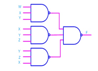
- Any logic function can be implemented using NAND gates.
- For this, the logic function has to be written in Sum of Product (SOP) form.
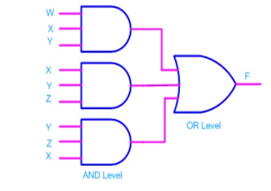
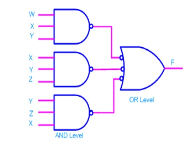
Consider the following SOP expression F = W.X.Y + X.Y.Z + Y.Z.W
The above expression can be implemented with three AND gates in first stage and one OR gate in second stage as shown in figure.
- If bubbles are introduced at AND gates output and OR gates input (the same for NOR gates), the above circuit becomes.
- Now replacing OR gate with input bubble with the NAND gate we have
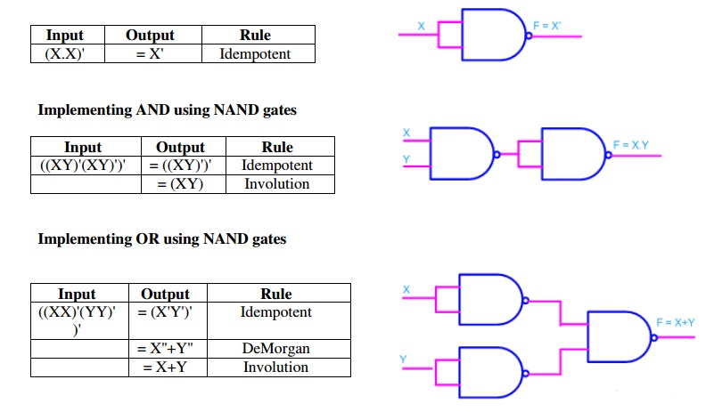
Realization of logic gates using NAND gates
Implementing an inverter using NAND gate

Realization of logic function using NOR gates
- Any logic function can be implemented using NOR gates.
- For this, the logic function has to be written in Product of Sum (POS) form
Consider the following POS expression F = (X+Y). (Y+Z)
- It can be implemented with three OR gates in first stage and one AND gate in second stage.

- If bubbles are introduced at the output of the OR gates and the inputs of AND gate, the above circuit comes out to be the next figure.
- Now replacing AND gate with input bubble with the NOR gate and we have circuit which is completely implemented with just NOR gates.
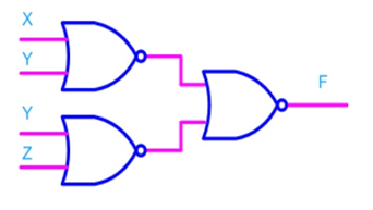
Implementing logic gates using NOR gate
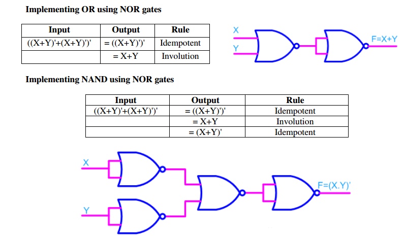
References:
1. Anand Kumar, “Fundamentals of Digital Circuits”, Prentice Hall of India, 1st Edition.
2. J. F. Wakerly, “Digital Design- Principles and Practices,”, Pearson, 3rd Edition.
3. M. M. Mano, “Digital Design,” Prentice Hall India.