Unit – 3
Combinational Circuits
- Half Adder
It is a combinational circuit which has two inputs and two outputs.
It is designed to add two single bit binary number A and B.
It has two outputs carry and sum.
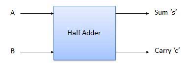
Fig.: Half adder
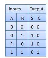
Fig: Truth Table
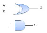
Fig: Circuit Diagram Half adder
Full Adder
- It is developed to overcome the drawback of Half Adder circuit.
- It can add two one-bit numbers A and B and a carry C.
- It is a three input and two output combinational circuit.
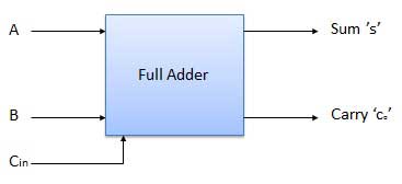
Fig: Block diagram Full adder
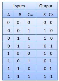
Fig: Truth Table
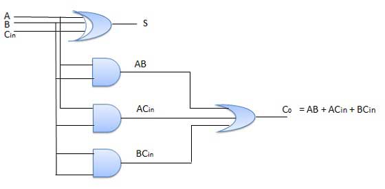
Fig: Circuit Diagram Full adder
Key Takeaways:
- Half adder is a combinational circuit which has two inputs and two outputs.
- Since there is no provision for carry in half adder, full adder is developed to overcome the drawback.
- Half Subtractors
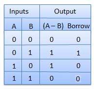
It is a combination circuit with two inputs and two outputs.
The difference between the two binary bits is obtained at the output and an output (Borrow) indicates if a 1 has been borrowed.
Here A is called as Minuend bit and B is called as Subtrahend bit.
Truth Table
Circuit Diagram
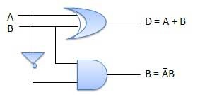
Half subtractor
B. Full Subtractors
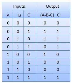
It is a combinational circuit which has three inputs A, B, C and two output D and C'.
A is the 'minuend', B is 'subtrahend', C is the 'borrow' which is produced by the previous stage, difference output D and C' is the borrow output.
Truth Table
Circuit Diagram
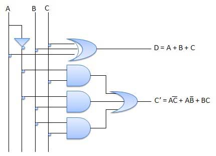
Full subtractor
Key Takeaways:
- Half subtractor is a combinational circuit which has two inputs and two outputs.
- Since there is no provision for borrow in half subtractor, full subtractor is developed to overcome the drawback.
A multiplier is a combinational logic circuit that we use to multiply binary digits. Just like the adder and the subtractor, a multiplier is an arithmetic combinational logic circuit. It is also known as a binary multiplier or a digital multiplier.
We use a multiplier in several digital signal processing applications. We use it to design calculators, mobiles, processors, and digital image processors.
It works just like normal multiplication. There are four main rules that are quite simple to understand:
0 x 0 = 0
0 x 1 = 0
1 x 0 = 0
1 x 1 = 1
Suppose you have two binary digits A1A0 and B1B0, here’s how that multiplication would take place
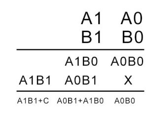
In the above calculation, A1A0 is the multiplicand. B1B0 is the multiplier. The first product obtained from multiplying B0 with the multiplicand is called as partial product 1. And the second product obtained from multiplying B1 with the multiplicand is known as the partial product 2.
As the number of bits increases, we keep shifting each successive partial product to the left by 1 bit. In the end, we add the digits while keeping in mind the carry that might generate.
Key Takeaways:
- A multiplier is a combinational logic circuit that we use to multiply binary digits.
- It is also known as a binary multiplier or a digital multiplier.
A comparator is a logic circuit, used to compare the magnitude of two binary numbers.
The following figure shows the block diagram of a n-bit comparator.
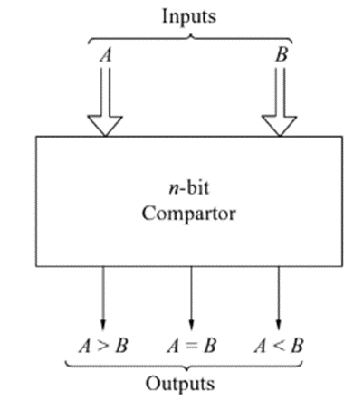
Fig.: Comparator
It receives two n-bit numbers A and B as inputs and the outputs are A>B, A=B and A<B. Depending upon the relative magnitude of the two numbers, one of the outputs will be high.
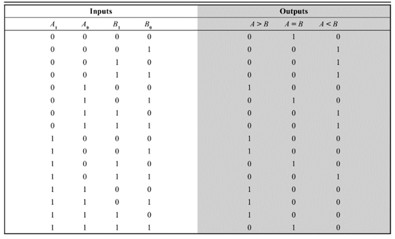
The following is the truth table of a 2-bit comparator.
- It works as an inverse of an encoder.
- It is a combinational circuit which converts n input lines into 2n output lines.
- Taking an example of 3-to-8-line decoder.
Truth Table –
X | Y | Z | D0 | D1 | D2 | D3 | D4 | D5 | D6 | D7 |
0 | 0 | 0 | 1 | 0 | 0 | 0 | 0 | 0 | 0 | 0 |
0 | 0 | 1 | 0 | 1 | 0 | 0 | 0 | 0 | 0 | 0 |
0 | 1 | 0 | 0 | 0 | 1 | 0 | 0 | 0 | 0 | 0 |
0 | 1 | 1 | 0 | 0 | 0 | 1 | 0 | 0 | 0 | 0 |
1 | 0 | 0 | 0 | 0 | 0 | 0 | 1 | 0 | 0 | 0 |
1 | 0 | 1 | 0 | 0 | 0 | 0 | 0 | 1 | 0 | 0 |
1 | 1 | 0 | 0 | 0 | 0 | 0 | 0 | 0 | 1 | 0 |
1 | 1 | 1 | 0 | 0 | 0 | 0 | 0 | 0 | 0 | 1 |
Implementation
D0 is high when X = 0, Y = 0 and Z = 0. Hence,
D0 = X’ Y’ Z’
Similarly,
D1 = X’ Y’ Z
D2 = X’ Y Z’
D3 = X’ Y Z
D4 = X Y’ Z’
D5 = X Y’ Z
D6 = X Y Z’
D7 = X Y Z
Hence,
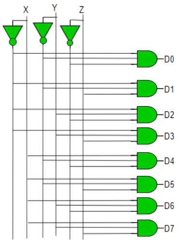
Fig: Decoder
Key Takeaways:
- It works as an inverse of an encoder.
- It is a combinational circuit which converts n input lines into 2n output lines.
- Binary code of N digits is used to store 2N distinct elements of coded information.
- This is the reason why encoders and decoders are used.
- Encoders convert 2N lines of input into a code of N bits and Decoders decode those N bits into 2N lines.
- Encoders –
- It is a combinational circuit that converts binary information in the form of a 2N input lines into N output lines, which represent N bit code for the input.
- For simple encoders, only one input line is active at a time.
- For example: Octal to Binary encoder takes 8 input lines and generates 3 output lines.
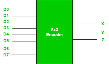
Fig.: 8X3 Encoder
Truth Table –
D7 | D6 | D5 | D4 | D3 | D2 | D1 | D0 | X | Y | Z |
0 | 0 | 0 | 0 | 0 | 0 | 0 | 1 | 0 | 0 | 0 |
0 | 0 | 0 | 0 | 0 | 0 | 1 | 0 | 0 | 0 | 1 |
0 | 0 | 0 | 0 | 0 | 1 | 0 | 0 | 0 | 1 | 0 |
0 | 0 | 0 | 0 | 1 | 0 | 0 | 0 | 0 | 1 | 1 |
0 | 0 | 0 | 1 | 0 | 0 | 0 | 0 | 1 | 0 | 0 |
0 | 0 | 1 | 0 | 0 | 0 | 0 | 0 | 1 | 0 | 1 |
0 | 1 | 0 | 0 | 0 | 0 | 0 | 0 | 1 | 1 | 0 |
1 | 0 | 0 | 0 | 0 | 0 | 0 | 0 | 1 | 1 | 1 |
- From the above truth table, it is seen that the output is 000 when D0 is active; 001 when D1 is active; 010 when D2 is active and so on.
Implementation –
- From the above truth table, the output Z is active when the input octal digit is 1, 3, 5 or 7.
- Y is active when input octal digit is 2, 3, 6 or 7 and X is active when input octal digits 4, 5, 6 or 7.
- Hence, the Boolean functions would be:
X = D4 + D5 + D6 + D7
Y = D2 +D3 + D6 + D7
Z = D1 + D3 + D5 + D7
- Hence, the encoder is realized with OR gates as follows:
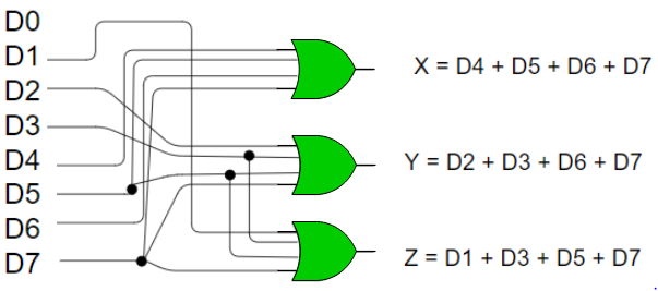
Fig: 8:3 encoder
- Limitation of the encoder is that only one input is active at a time.
- If more than one input is active, then the output of encoder is undefined.
- For example, if D6 and D3 are both active, then, our output would be 111 which is the output for D7.
- Problem arises when all inputs are 0.
- The encoder gives output 000 which actually is the output for D0. To avoid this, an extra bit is added to the output which is called the valid bit whose value is 0 when all inputs are 0 or 1.
Priority Encoder:
- It is an encoder whose inputs are given priorities.
- When more than one input becomes active at the same time then the input with higher priority takes precedence w.r.to the output which is generated.
- Considering a 4:2 priority encoder.
- From the truth table given below we see that when all inputs are 0, V bit is zero and outputs are not used.
- The x in the table shows the don’t care condition, i.e. it can be 0 or 1.
- Here, D3 has highest priority, therefore, when D3 is high, output has to be 11.
- D0 has the lowest priority, hence the output would be 00 only when D0 is high and all the other input lines are low.
Truth Table –
D3 | D2 | D1 | D0 | X | Y | V |
0 | 0 | 0 | 0 | x | x | 0 |
0 | 0 | 0 | 1 | 0 | 0 | 1 |
0 | 0 | 1 | x | 0 | 1 | 1 |
0 | 1 | X | x | 1 | 0 | 1 |
1 | x | X | x | 1 | 1 | 1 |
Implementation
The condition for valid bit to be 1 is when at least one of the inputs should be high. Hence,
V = D0 + D1 + D2 + D3
For X:
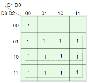
=>X=D2+D3
For Y:
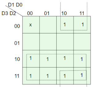
=> Y = D1 D2’ + D3
Hence, the priority 4-to-2 encoder can be realized as follows:
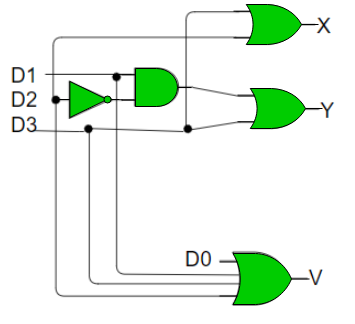
Fig: Priority encoder
Key takeaway
An Encoder is a combinational circuit that performs the reverse operation of Decoder. It has maximum of 2n input lines and ‘n’ output lines. It will produce a binary code equivalent to the input, which is active High.
- It is a special type of combinational circuit.
- It has n-data inputs, one output and m inputs select lines with 2m = n.
- It selects one of the n data inputs and routes it to the output.
- The selection of one of the inputs is done by the select lines.
- Depending on the code applied at the inputs, one of the n data sources is selected and transmitted to the single output Y.
- E is the enable input which is useful for cascading purpose.
- It is an active low terminal hence performs the required operation when it is low.
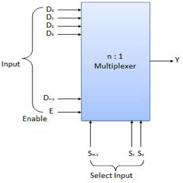
Fig.: Block diagram of multiplexer
Multiplexers come in multiple variations
- 2: 1 multiplexer
- 4: 1 multiplexer
- 16: 1 multiplexer
- 32: 1 multiplexer
Block Diagram of 2:1 MUX
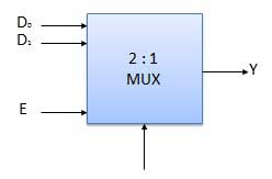
Fig.: 2:1 MUX
Truth Table of 2:1 MUX
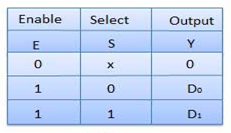
Where x is don’t care.
Key Takeaways
- It has n-data inputs, one output and m inputs select lines with 2m = n.
- The selection of one of the inputs is done by the select lines.
- It performs the inverse operation of a multiplexer as it receives one input and distributes it across its outputs.
- It has only one input and n outputs with m select input.
- At a time only one output line is selected by the select lines and that input is transmitted through the output line.
- It is equivalent to a single pole multiple way switch.
Various Demultiplexers are used as:
- 1: 2 demultiplexer
- 1: 4 demultiplexer
- 1: 16 demultiplexer
- 1: 32 demultiplexer
Block diagram
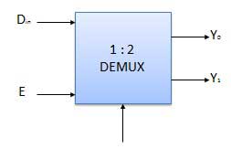
Truth Table
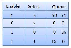
Where x is don’t care.
Key Takeaways:
- It performs the inverse operation of a multiplexer as it receives one input and distributes it across its outputs.
- It has only one input and n outputs with m select input.
SOP function and a multiplexer is given.
There are certain steps to implement the given SOP function using the given MUX:
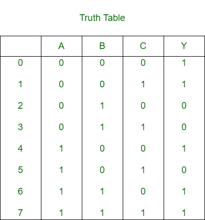
Step 1: Draw the truth table for the given number of variable functions.
Step 2: Consider one variable as input and remaining variables as select lines.
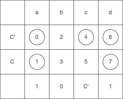
Step 3: Form a matrix where input lines of MUX are columns and input variable and its compliment are rows.
Step 4: Find AND between both rows on the basis of the truth table.
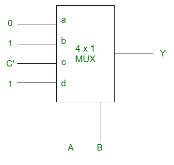
Step 5: Hence whatever is found is considered as input of MUX.
We will illustrate it with an example:
Example:
Given SOP function f(A, B, C) = m(0, 1, 4, 6, 7) and MUX is
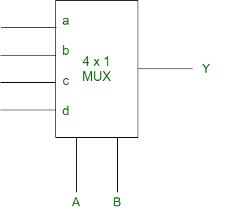
For 3 variable functions, the truth table is
Let A and B are the select lines and C be the input,
Thus, for the implementation of given logical function, required is one 4×1 MUX and inverter.
- The parity generating technique is used as error detection technique for the data transmission.
- When binary data is transmitted and processed, it is subjected to noise and that noise can alter 0s to 1s and 1s to 0s of data bits in digital systems.
- Therefore, a parity generator is a combinational logic circuit that generates the parity bit at the transmitter end.
- The basic principle is that sum of odd number of 1s is always 1 and sum of even number of 1s is always zero.
- Such error detection and correction can be implemented by using Ex-OR gates.
Even Parity Generator
A 3-bit message is transmitted with an even parity bit. Hence assuming, the three inputs W, X and Y that are applied to the circuits and output bit is the parity bit P. The total number of 1s must be even, to generate the even parity bit P.
3- bit message | Even Parity | ||
W | X | Y | P |
0 | 0 | 0 | 0 |
0 | 0 | 1 | 1 |
0 | 1 | 0 | 1 |
0 | 1 | 1 | 0 |
1 | 0 | 0 | 1 |
1 | 0 | 1 | 0 |
1 | 1 | 0 | 0 |
1 | 1 | 1 | 1 |
The K-map simplification for 3-bit message even parity generator is
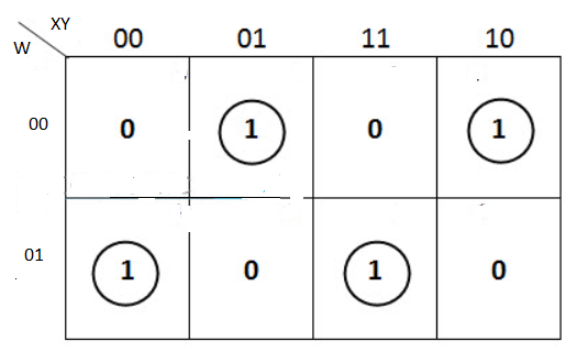
From the above K-Map, the expression is:
P=W′X′Y+W′XY′+WX′Y′+WXY
P=W′(X′Y+XY′) +W(X′Y′+XY)
P=W′(X⊕Y) +W(X⊕Y) ′=W⊕X⊕Y

Odd Parity Generator
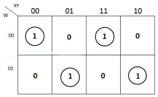
Considering that the 3-bit data is transmitted with an odd parity bit. The three inputs are W, X and Y and P is the output parity bit. The total number of bits must be odd in order to generate the odd parity bit.
3- bit message | Odd Parity | ||
W | X | Y | P |
0 | 0 | 0 | 1 |
0 | 0 | 1 | 0 |
0 | 1 | 0 | 0 |
0 | 1 | 1 | 1 |
1 | 0 | 0 | 0 |
1 | 0 | 1 | 1 |
1 | 1 | 0 | 1 |
1 | 1 | 1 | 0 |
The K-map simplification for 3-bit message even parity generator is

Binary To Gray Code
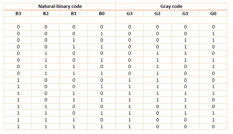
For this circuit, B3 B2 B1 B0 are inputs while G3 G2 G1 G0 are outputs.
K-map for the outputs:
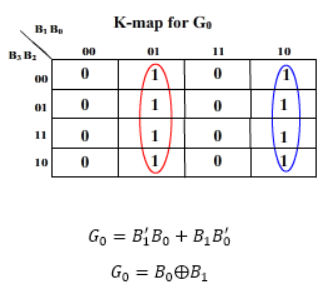
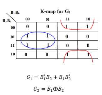
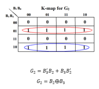
And G3 = B3
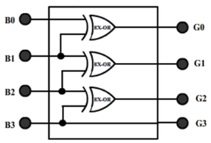
2. Gray to Binary Code
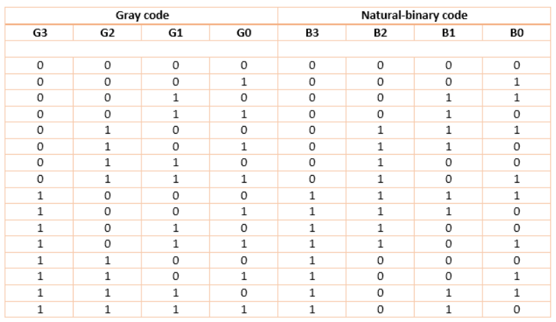
Then the K-maps:
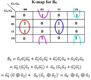
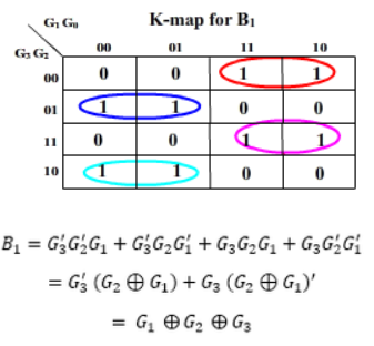
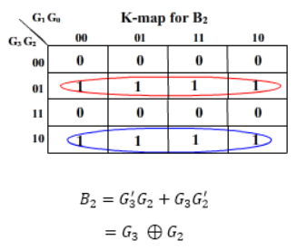
And B3 = G3
The realization of Gray-to-Binary converter is
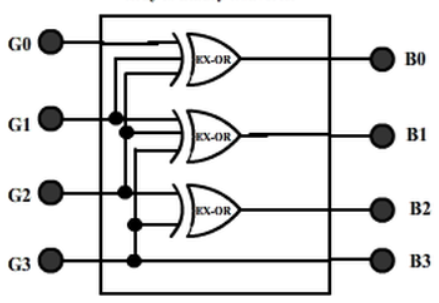
Key Takeaways:
- These are the combinational circuits made by conversion of one code to another.
A hazard, if exists, in a digital circuit causes a temporary fluctuation in output of the circuit. In other words, a hazard in a digital circuit is a temporary disturbance in ideal operation of the circuit which if given some time, gets resolved itself. These disturbances or fluctuations occur when different paths from the input to output have different delays and due to this fact, changes in input variables do not change the output instantly but do appear at output after a small delay caused by the circuit building elements, i.e., logic gates.
There are three different kinds of hazards found in digital circuits
- Static hazard
- Dynamic hazard
- Functional hazard
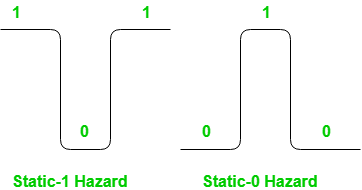
Formally, a static hazard takes place when change in an input causes the output to change momentarily before stabilizing to its correct value. Based on what is the correct value, there are two types of static hazards, as shown below in the image:
- Static-1 Hazard: If the output is currently at logic state 1 and after the input changes its state, the output momentarily changes to 0 before settling on 1, then it is a Static-1 hazard.
- Static-0 Hazard: If the output is currently at logic state 0 and after the input changes its state, the output momentarily changes to 1 before settling on 0, then it is a Static-0 hazard.
Detection of Static hazards using K-map:
To detect a static-1 hazard for a digital circuit following steps are used:
- Step-1: Write down the output of the digital circuit, say Y.
- Step-2: Draw the K-map for this function Y and note all adjacent 1’s.
- Step-3: If there exists any pair of cells with 1’s which do not occur to be in the same group (i.e., prime implicant), it indicates the presence of a static-1 hazard. Each such pair is a static-1 hazard.
Example – Consider the circuit shown below.
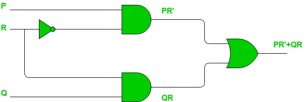
We have output, say F, as:
Lets draw the K-map for this Boolean function as follows:
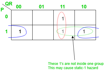
The pair of 1’s encircled as green are not part of the grouping/pairing provided by the output of this Boolean function. This will cause a static-1 hazard in this circuit.
Removal of static-1 hazard:
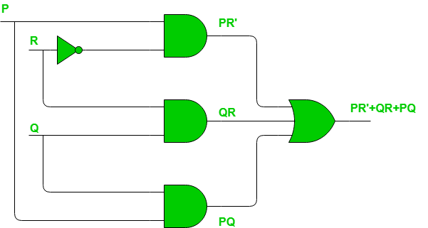
Once detected, a static-1 hazard can be easily removed by introducing some more terms (logic gates) to the function (circuit). The most common idea is to add the missing group in the existing Boolean function, as adding this term would not affect the function by any mean but it will remove the hazard. Since in above example the pair of 1’s encircled with blue color causes the static-1 hazard, we just add this as a prime implicant to the existing function as follows:
Note that there is no difference in number of minterms of this function. The reason is that the static-1 hazards are based on how we group 1’s (or 0’s for static-0 hazard) for a given set of 1’s in K-map. Thus, it does not make any difference in number of 1’s in K-map. The circuit would look like as shown below with the change made for removal of static-1 hazard.
Similarly for Static-0 Hazards we need to consider 0’s instead of 1’s and if any adjacent 0’s in K-map is not grouped into same group that may cause a static-0 hazard. The method to detect and resolve the static-0 hazard is completely same as the one we followed for static-1 hazard except that instead of SOP, POS will be used as we are dealing with 0’s in this case.
References:
1. Anand Kumar, “Fundamentals of Digital Circuits”, Prentice Hall of India, 1st Edition.
2. J. F. Wakerly, “Digital Design- Principles and Practices,”, Pearson, 3rd Edition.
3. M. M. Mano, “Digital Design,” Prentice Hall India.