Unit – 4
Synchronous Sequential Circuits
A synchronous sequential circuit is also called as Finite State Machine FSM, if it has finite number of states. There are two types of FSMs.
- Mealy State Machine
- Moore State Machine
Mealy Machine
A Mealy Machine is an FSM whose output depends on the present state as well as the present input.
It can be described by a 6 tuple (Q, ∑, O, δ, X, q0) where −
- Q is a finite set of states.
- ∑ is a finite set of symbols called the input alphabet.
- O is a finite set of symbols called the output alphabet.
- δ is the input transition function where δ: Q × ∑ → Q
- X is the output transition function where X: Q × ∑ → O
- q0 is the initial state from where any input is processed (q0 ∈ Q).
The state table of a Mealy Machine is shown below −
Present state | Next state | |||
Input = 0 | Input = 1 | |||
State | Output | State | Output | |
→ a | b | x1 | c | x1 |
b | b | x2 | d | x3 |
c | d | x3 | c | x1 |
d | d | x3 | d | x2 |
The state diagram of the above Mealy Machine is −
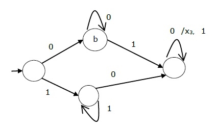
Moore Machine
Moore machine is an FSM whose outputs depend on only the present state.
A Moore machine can be described by a 6 tuple (Q, ∑, O, δ, X, q0) where −
- Q is a finite set of states.
- ∑ is a finite set of symbols called the input alphabet.
- O is a finite set of symbols called the output alphabet.
- δ is the input transition function where δ: Q × ∑ → Q
- X is the output transition function where X: Q → O
- q0 is the initial state from where any input is processed (q0 ∈ Q).
The state table of a Moore Machine is shown below −
Present state | Next State | Output | |
Input = 0 | Input = 1 | ||
→ a | b | c | x2 |
b | b | d | x1 |
c | c | d | x2 |
d | d | d | x3 |
The state diagram of the above Moore Machine is −
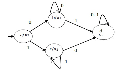
Mealy Machine vs. Moore Machine
The following table highlights the points that differentiate a Mealy Machine from a Moore Machine.
Mealy Machine | Moore Machine |
Output depends both upon the present state and the present input | Output depends only upon the present state. |
Generally, it has fewer states than Moore Machine. | Generally, it has more states than Mealy Machine. |
The value of the output function is a function of the transitions and the changes, when the input logic on the present state is done. | The value of the output function is a function of the current state and the changes at the clock edges, whenever state changes occur. |
Mealy machines react faster to inputs. They generally react in the same clock cycle. | In Moore machines, more logic is required to decode the outputs resulting in more circuit delays. They generally react one clock cycle later. |
Latches
- In digital electronics, a Latch is one kind of a logic circuit, and it is also known as a bistable-multivibrator. Because it has two stable states namely active high as well as active low.
- It works like a storage device by holding the data through a feedback lane.
- It stores 1-bit of data as long as the apparatus is activated. Once enable is declared then instantly latch can change the stored data. It constantly trials the inputs once enable signal is activated.
- The working of these circuits can be done in 2-states based on the enable signal being high or else low. When the latch circuit is the in an active high state, then both the i/ps are low. Similarly, when the latch circuit is then an active low state, then both the i/ps are high.
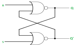
SR Latch is a circuit which has:
(i) 2 cross-coupled NOR gate or NAND gate.
(ii) 2 input S for SET and R for RESET.
(iii) 2 output Q and Q’.
Q | Q’ | STATE |
1 | 0 | Set |
0 | 1 | Reset |
Under normal conditions, both the input remains 0.
RS Latch with NAND gates:
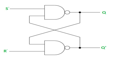
Case-1: When S’=R’=1 or S=R=0 then
If Q = 1, Q = R’ = 1.
If Q = 0, Q = 0 and R’ = 1 respectively.
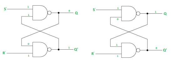
Case-2: S’=0, R’=1 (S=1, R=0)
As S’=0, Q = 1(SET state).
In 2nd NAND gate, as Q = R’ = 1, Q’=0.
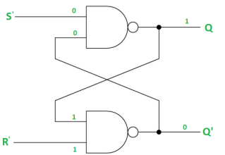
Case-3: S’= 1, R’= 0 (S=0, R=1)
As R’=0, Q’ = 1.
In 1st NAND gate, as Q =S’ = 1, Q=0 (RESET state).
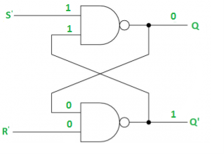
Case-4: S’= R’= 0 (S=R=1)
When S=R=1, both Q = Q’ = 1 which is not allowed.
So, this input condition is prohibited.
The SR Latch using NOR gate is:
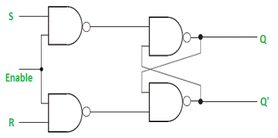
Gated SR Latch –
It is a latch which enable input that works when enable = 1 and retain the previous state when enable = 0.
Gated D Latch –
It is similar to SR latch with little modifications. Here, the inputs are complements of one another. The design of D latch with Enable signal is given below:
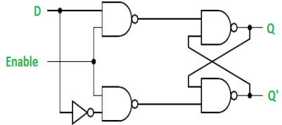
The truth table is shown below:
ENABLE | D | Q(N) | Q(N+1) | STATE |
1 | 0 | x | 0 | RESET |
1 | 1 | x | 1 | SET |
0 | x | x | Q(n) | No Change |
As the output is same as input, it is also known as Transparent Latch.
The characteristic equation for D latch with enables input is given as:
Q(n+1) = EN.D + EN'.Q(n)
Flip-flops
S-R Flip Flop:
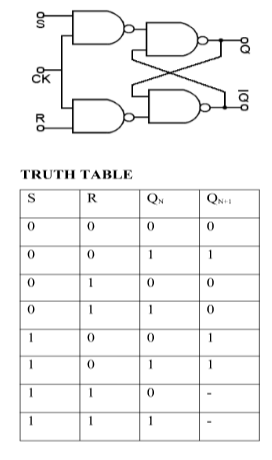
J-K Flip Flop:
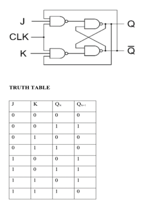
Race Around Condition in JK Flip-flop –
- For J-K flip-flop, if J=K=1, and if clk=1 for a long period of time, then output Q will toggle as long as CLK remains high which makes the output unstable or uncertain.
- This problem is known as race around condition in J-K flip-flop.
- This problem can be avoided by ensuring that the clock input is at logic “1” only for a very short time.
- Hence the concept of Master Slave JK flip flop was introduced.
Master Slave JK flip flop –
It is basically a combination of two JK flip-flops connected together in series.
The first is the “master” and the other is a “slave”.
The output from the master is connected to the two inputs of the slave whose output is fed back to inputs of the master.
In addition to these two flip-flops, the circuit comprises of an inverter.
The inverter is connected to clock pulse in such a way that an inverted clock pulse is given to the slave flip-flop.
In other words, if CP=0 for a master flip-flop, then CP=1 for a slave flip-flop and vice versa.
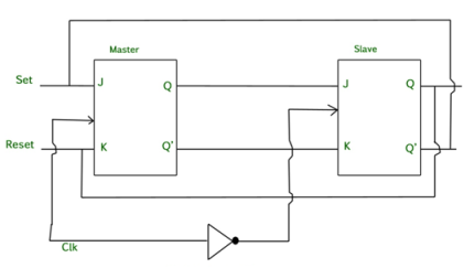
Fig. Master Slave Flip flop
Working of a master slave flip flop –
- When the clock pulse goes high, the slave is isolated; J and K inputs can affect the state of the system. The slave flip-flop is isolated when the CP goes low. When the CP goes back to 0, information is transmitted from the master flip-flop to the slave flip-flop and output is obtained.
- The master flip flop is positive level triggered and the slave flip flop is negative level triggered, hence the master responds prior to the slave.
- If J=0 and K=1, Q’ = 1 then the master goes to the K input of the slave and the clock forces the slave to reset therefore the slave copies the master.
- If J=1 and K=0, Q = 1 then the master goes to the J input of the slave and the Negative transition of the clock sets the slave and thus copy the master.
- If J=1 and K=1, the master toggles on the positive transition and the slave toggles on the negative transition of the clock.
- If J=0 and K=0, the flip flop becomes disabled and Q remains unchanged.
Timing Diagram of a Master flip flop –
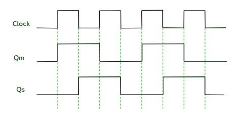
- When the CP = 1 then the output of master is high and remains high till CP = 0 because the state is stored.
- Now the output of master becomes low when the clock CP = 1 and remains low until the clock becomes high again.
- Thus, toggling takes place for a clock cycle.
- When the CP = 1 then the master is operational but not the slave.
- When the clock is low, the slave becomes operational and remains high until the clock again becomes low.
- Toggling takes place during the whole process since the output changes once in a cycle.
- This makes the Master-Slave J-K flip flop a Synchronous device which passes data with the clock signal.
D Flip Flop:
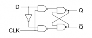
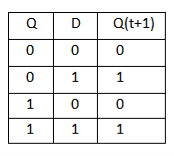
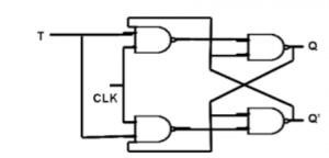
T Flip Flop:
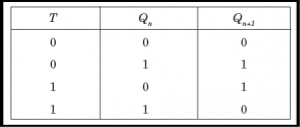
- Some flip-flops have asynchronous inputs that are used to force the flip-flop to a particular state independently of the clock
- The input that sets the flip-flop to 1 is called preset or direct set. The input that clears the flip-flop to 0 is called clear or direct reset.
- When power is turned on in a digital system, the state of the flip-flops is unknown. The direct inputs are useful for bringing all flip-flops in the system to a known starting state prior to the clocked operation.
- The knowledge of the type of flip-flops and a list of the Boolean expressions of the combinational circuit provide the information needed to draw the logic diagram of the sequential circuit. The part of the combinational circuit that gene rates external outputs is described algebraically by a set of Boolean functions called output equations. The part of the circuit that generates the inputs to flip-flops is described algebraically by a set of Boolean functions called flip-flop input equations (or excitation equations).
- The information available in a state table can be represented graphically in the form of a state diagram. In this type of diagram, a state is represented by a circle and the (clock-triggered) transitions between states are indicated by directed lines connecting the circles.
- The time sequence of inputs, outputs, and flip-flop states can be enumerated in a state table (transition table). The table has four parts present state, next state, inputs and outputs.
- In general, a sequential circuit with 'm' flip-flops and 'n' inputs needs 2m+n rows in the state table.
Positive Edge Triggered D Flip-flop
- A circuit diagram of a Positive edge triggered D Flip-flop is shown as below. It has an additional reset input connected to the three NAND gates.
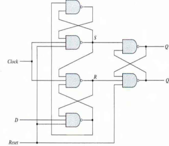
Fig: Circuit Diagram
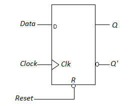
Fig: Symbol
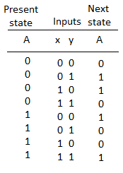
Fig: State Table
- When the reset input is 0 it forces output Q' to Stay at 1 which clears output Q to 0 thus resetting the flip-flop.
- Two other connections from the reset input ensure that the S input of the third SR latch stays at logic 1 while the reset input is at 0 regardless of the values of D and Clk.
- Function table suggests that:
- When R = 0, the output is set to 0 (independent of D and Clock).
- The clock at Clock is shown with an upward arrow to indicate that the flip-flop triggers on the positive edge of the clock.
- The value in D is transferred to Q with every positive-edge clock signal provided that R = 1.
Analysis with D Flip-Flops
- The input equation of a D Flip-flop is given by DA = A ⊕ x ⊕ y. DA means a D Flip-flop with output A.
- The x and y variables are the inputs to the circuit. No output equations are given, which implies that the output comes from the output of the flip-flop.
- The state table has one column for the present state of flip-flop 'A' two columns for the two inputs, and one column for the next state of A.
- The next-state values are obtained from the state equation A (t + 1) = A ⊕ x ⊕ y.
- The expression specifies an odd function and is equal to 1 when only one variable is 1 or when all three variables are 1.
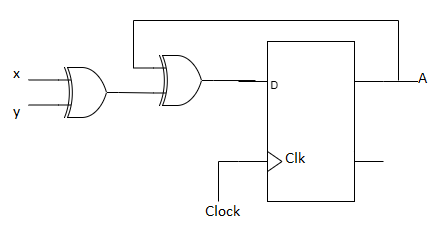
Fig: Circuit Diagram
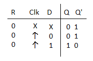
Fig: State Table
Analysis with JK Flip-Flops
- The circuit can be specified by the flip-flop input equations:
- JA = B; KA = Bx'
- JB = x'; KB = A'x + Ax' = A ⊕ x
- The next state of each flip-flop is evaluated from the corresponding J and K inputs and the characteristic table of the JK flip-flop listed as:
- When J = 1 and K = 0 the next state is 1
- When J = 0 and K = 1 the next state is 0
- When J = 0 and K = 0 there is no change of state and the next-state value is the same as that of the present state.
- When J = K = 1, the next-state bit is the complement of the present-state bit.
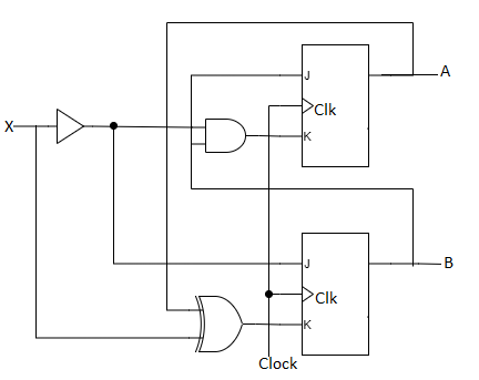
Fig: Circuit Diagram
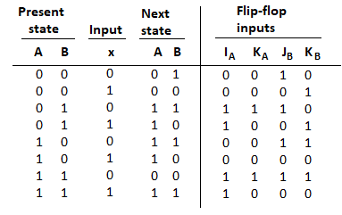
Fig: State Table
- The characteristic equations for the flip-flops are
- A (t + 1) = JA' + K'A
- B (t + 1) = JB' + K'B
- This gives us the state equation of A by substituting the values of JA, KA
A (t + 1) = BA' + (Bx')'A = A'B + AB' + Ax
- The state equation provides the bit values for the column headed "Next State" for A in the state table. Similarly, the state equation for flip-flop B can be derived from the characteristic equation by substituting the values of JB and KB.:
- B (t + 1) = x'B' + (A ⊕ x)'B = B'x' + ABx + A'Bx'
Analysis with T Flip-Flops
- The circuit can be specified by the characteristic equations:
- Q(t+1) = T ⊕ Q = T'Q + TQ'
- The sequential circuit has two flip-flops A and B, one input x, and one output y and can be described algebraically by two input equations and an output equation.
- TA = Bx
- TB = x
- y = AB
- The state table for the circuit is listed below. The values for y are obtained from the output equation. The values for the next state can be derived from the state equations by substituting TA and TB in the characteristic equations yielding:
- A (t + 1) = (Bx)' A + (Bx)A' = AB' + Ax' + A'Bx
- B (t + 1) = x ⊕ B
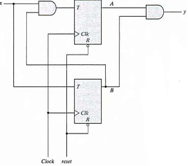
Fig: Circuit Diagram
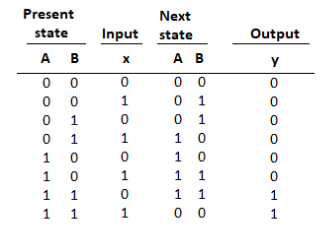
Fig: State Table
An algorithm for the state reduction quotes that:
“Two states are said to be equivalent if, for each member of the set of inputs, they give exactly the same output and send the circuit either to the same state or to an equivalent state.”
Now apply this algorithm to the state table of the circuit:
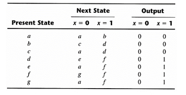
States g and e both go to states a and f and have outputs of 0 and 1 for x = 0 and x = 1, respectively.
The procedure for removing a state and replacing it by its equivalent is demonstrated in the following table:
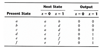
Thus, the row with present state g is removed and stage g is replaced by state e each time it occurs in the next state columns. Present state f now has next states e and f and outputs 0 and 1 for x = 0 and x = 1. The same next states and outputs appear in the row with present state d. Therefore, states f and d are equivalent and can be removed and replaced with d.
The final reduced state table is:
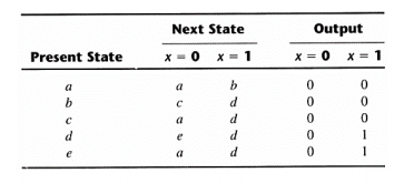
The state diagram for the above reduced table is:
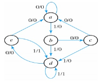
This state diagram satisfies the original input output specifications.
Applying the input sequence previously used, the following list is obtained:

Note that the same output sequence results, although the state sequence is different.
It counts ten different states and then reset to its initial states.
A simple decade counter will count from 0 to 9 but the decade counters which can go through any ten states between 0 to 15(for 4-bit counter) can also be made.
Truth table is as follows:
Clock pulse | Q3 | Q2 | Q1 | Q0 |
0 | 0 | 0 | 0 | 0 |
1 | 0 | 0 | 0 | 1 |
2 | 0 | 0 | 1 | 0 |
3 | 0 | 0 | 1 | 1 |
4 | 0 | 1 | 0 | 0 |
5 | 0 | 1 | 0 | 1 |
6 | 0 | 1 | 1 | 0 |
7 | 0 | 1 | 1 | 1 |
8 | 1 | 0 | 0 | 0 |
9 | 1 | 0 | 0 | 1 |
10 | 0 | 0 | 0 | 0 |
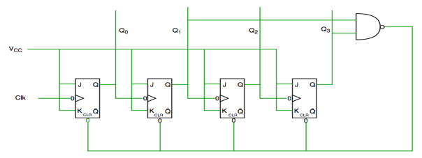
Fig 5 Decade counter
In the above circuit diagram, we used NAND gate for Q3 and Q1 and sending this to clear input line as the binary representation of 10 is—
1010
And Q3 and Q1 are 1 here, if we give NAND of these two bits then counter clears at 10 and again starts from the beginning.
Up/down counters
Both Synchronous and Asynchronous counters are capable of counting “Up” or counting “Down”, but there is another more “Universal” type of counter that can count in both directions either up or down depending on the state of their input control pin and these are known as Bidirectional Counters.
Bidirectional counters, also known as Up/Down counters, are capable of counting in either direction through any given count sequence and they can be reversed at any point within their count sequence by using an additional control input as shown below.
The circuit above is of a simple 3-bit Up/Down synchronous counter using JK flip-flops configured to operate as toggle or T-type flip-flops giving a maximum count of zero (000) to seven (111) and back to zero again. Then the 3-Bit counter advances upward in sequence (0,1,2,3,4,5,6,7) or downwards in reverse sequence (7,6,5,4,3,2,1,0).
Generally, most bidirectional counter chips can be made to change their count direction either up or down at any point within their counting sequence. This is achieved by using an additional input pin which determines the direction of the count, either Up or Down and the timing diagram gives an example of the counter’s operation as this Up/Down input changes state.
Nowadays, both up and down counters are incorporated into single IC that is fully programmable to count in both an “Up” and a “Down” direction from any preset value producing a complete Bidirectional Counter chip. Common chips available are the 74HC190 4-bit BCD decade Up/Down counter, the 74F569 is a fully synchronous Up/Down binary counter and the CMOS 4029 4-bit Synchronous Up/Down counter.
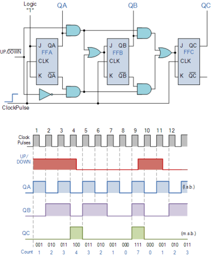
Fig: Up/Down Counter
Key takeaway
Both Synchronous and Asynchronous counters are capable of counting “Up” or counting “Down”, but there is another more “Universal” type of counter that can count in both directions either Up or Down depending on the state of their input control pin and these are known as Bidirectional Counters.
Ring counters
- It is a shift register counter whose output of the first flip flop is connected to the second and so on and the output of the last flip flop is fed back to the input of the first flip flop, thus named as ring counter.
- The data pattern in the register circulates as long as clock pulses are applied.
- The circuit below comprises of four D flip-flops which are connected synchronously.
- The data pattern repeats after every four clock pulses shown in the truth table.
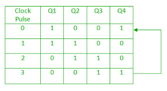

Fig. Ring counter
- It is self-decoding.
- Hence no extra decoding circuit is required to determine which state the counter is in.
Key takeaway
It is a shift register counter whose output of the first flip flop is connected to the second and so on and the output of the last flip flop is fed back to the input of the first flip flop, thus named as ring counter.
Serial binary adder is a combinational logic circuit that performs the addition of two binary numbers in serial form. Serial binary adder performs bit by bit addition. Two shift registers are used to store the binary numbers that are to be added.
A single full adder is used to add one pair of bits at a time along with the carry. The carry output from the full adder is applied to a D flip-flop. After that output is used as carry for next significant bits. The sum bit from the output of the full adder can be transferred into a third shift register.
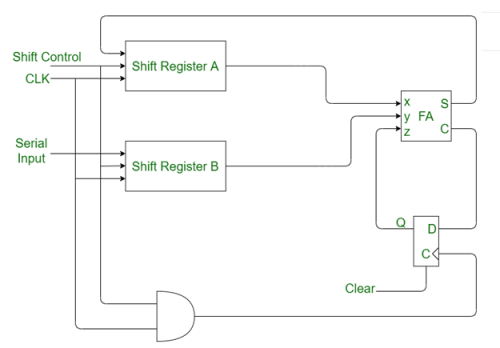
Fig: Block diagram of Serial Binary Adder
References:
1. Anand Kumar, “Fundamentals of Digital Circuits”, Prentice Hall of India, 1st Edition.
2. J. F. Wakerly, “Digital Design- Principles and Practices,”, Pearson, 3rd Edition.
3. M. M. Mano, “Digital Design,” Prentice Hall India.