Unit - 2
Small Signal Analysis of BJTs and FETs
The hybrid two port model is shown below.
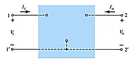
Fig 1 hybrid model
Vi = h11Ii + h12Vo
Io = h21Ii + h22Vo
h11 = hi = Vi/Io for Vo =0 [Input resistance]
h12 = hr = Vi/Vo for Ii =0 [Reverse voltage gain]
h21 = hf = Io/Ii for Vo =0 [forward current gain]
h22 = ho = Io/Vo for Ii =0 [output admittance]
The hybrid equivalent model is shown below

Fig 2 Equivalent hybrid model
The transistor model has three terminals with two ports.
hi = input resistance
ho= output conductance
hr= Vi/Vo = reverse transfer voltage
hf= Io/Ii = forward transfer current ratio
The simplified model is shown below
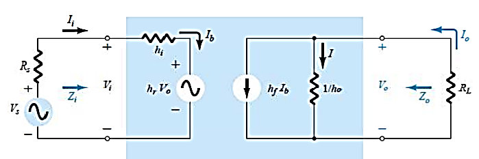
Fig 3 Simplified Model
Finding current gain Ai
Applying KCL at the output of above circuit
Io =I + hf Ib = Vo ho + hf Ib
Vo = -Io RL
Io = -Io RL ho + hf Ib
Io (1 + RL ho) = hf Ib
Ai = Io/ Ib = hf/ (1 + RL ho)
Finding Voltage Gain AV
Applying KVL at input of the above h-model
Vi = hi Ib + hr Vo
But Ib = (1 + ho RL)/hf
Io = - Vo/RL
Substituting in above equation and solving for Vo/Vi we get
Av = - hf RL/hi + (hi ho- hf hr) RL
Finding Input Impedance Zi
Vi = hi Ib + hr Vo
Io = - Vo/RL
Ai = Io/ Ib
Vi = hi Ib - hrRLAiIb
Zi = Vi/Ib = hi - hrRLAi
Finding Output impedance Zo
It is ratio of output voltage to output current with Vs =0
Io = Voho + hfIb
Ii = -hrVo/Rs + hi
Zo = Vo/Io = 1/ [ho – (hfhr/hi+ Rs)]
Key takeaway
CE to CB h-parameters | CE to CC h-parameters | CE h-parameters To r-parameters |
|
|
|
Small Signal Analysis of CE Amplifiers
In most practical cases it is appropriate to obtain approximate values of AV, Ai etc rather than calculating exact values. How the circuit can be modified without greatly reducing the accuracy. Figure shows the CE amplifier equivalent circuit in terms of h-parameters Since 1 / hoe in parallel with RL is approximately equal to RL if 1 / hoe >> RL then hoe may be neglected. Under these conditions.
Ic = hfe IB.
hre vc = hre Ic RL = hre hfe Ib RL
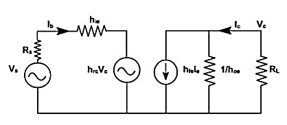
Fig 4 CE Amplifiers
Since hfe hre » 0.01, this voltage may be neglected in comparison with hic Ib drop across hie provided RL is not very large. If load resistance RL is small than hoe and hre can be neglected.
Ai = Io/ Ib = hfe/ (1 + RL hoe)
Ri= hie
Av= AIRL/Ri= -hfe RL/hie
Output impedance seems to be infinite. When Vs = 0, and an external voltage is applied at the output we fined Ib = 0, IC = 0. True value depends upon RS and lies between 40 K and 80K. On the same lines, the calculations for CC and CB can be done.
CE amplifier with an emitter resistor:
The voltage gain of a CE stage depends upon hfe. This transistor parameter depends upon temperature, aging and the operating point. Moreover, hfe may vary widely from device to device, even for same type of transistor. To stabilize voltage gain AV of each stage, it should be independent of hfe. A simple and effective way is to connect an emitter resistor Re as shown in figure. The resistor provides negative feedback and provide stabilization.
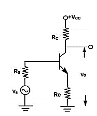
Fig 5 CE amplifier with an emitter resistor
Current gain Ai =  =
=  =
= 
Input Resistance is given by
Ri = 
= 
= hfe = (1+ hfe) Re
The input resistance is increased by (1+hfe) Re
Ai =  =
= 
Ai =  =
= 
CE amplifiers are very popular to amplify the small signal ac. After a transistor has been biased with a Q point near the middle of a dc load line, ac source can be coupled to the base. This produces fluctuations in the base current and hence in the collector current of the same shape and frequency. The output will be enlarged sine wave of same frequency. The amplifier is called linear if it does not change the wave shape of the signal.
As long as the input signal is small, the transistor will use only a small part of the load line and the operation will be linear. On the other hand, if the input signal is too large. The fluctuations along the load line will drive the transistor into either saturation or cut off. This clips the peaks of the input and the amplifier is no longer linear.
The CE amplifier configuration is shown
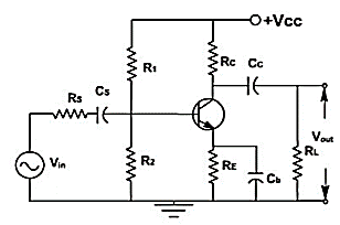
Fig 6 CE Amplifier Circuit
The coupling capacitor (CC) passes an ac signal from one point to another. At the same time, it does not allow the dc to pass through it. Hence it is also called blocking capacitor.
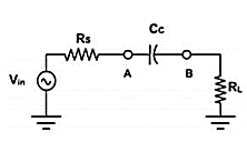
Fig 7 Coupling Capacitor
From Figure above the ac voltage at point A is transmitted to point B. For this series reactance XC should be very small compared to series resistance RS. The circuit to the left of A may be a source and a series resistor or may be the Thevenin equivalent of a complex circuit. Similarly, RL may be the load resistance or equivalent resistance of a complex network. The current in the loop is given by
i = 
= 
As frequency increases, XC decreases, and current increases until it reaches to its maximum value vin / R. Therefore, the capacitor couples the signal properly from A to B when XC<< R. The size of the coupling capacitor depends upon the lowest frequency to be coupled. Normally, for lowest frequency XC 0.1R is taken as design rule. The coupling capacitor acts like a switch, which is open to dc and shorted for ac. The bypass capacitor Cb is similar to a coupling capacitor, except that it couples an ungrounded point to a grounded point. The Cb capacitor looks like a short to an ac signal and therefore emitter is said ac grounded. A bypass capacitor does not disturb the dc voltage at emitter because it looks open to dc current. As a design rule XCb =0.1RE at
Analysis of CE amplifier: In a transistor amplifier, the dc source sets up quiescent current and voltages. The ac source then produces fluctuations in these current and voltages. The simplest way to analyse this circuit is to split the analysis in two parts: dc analysis and ac analysis. One can use superposition theorem for analysis.
Characteristics of Common Emitter Amplifier
(i) The current gain Ai is high for RL < 10 kΩ.
(ii) The voltage gain is high for normal values of load resistance RL.
(iii) The input resistance Ri is medium.
(iv) The output resistance Ro is moderately high.
Applications: CE amplifier is widely used for amplification
Common Base Amplifier
The common base amplifier circuit is shown in Figure below. The VEE source forward biases the emitter diode and VCC source reverse biased collector diode. The ac source vin is connected to emitter through a coupling capacitor so that it blocks dc.
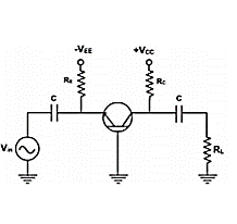
Fig 8 CB Amplifier
This ac voltage produces small fluctuation in currents and voltages. The load resistance RL is also connected to collector through coupling capacitor so the fluctuation in collector base voltage will be observed across RL. The dc equivalent circuit is obtained by reducing all ac sources to zero and opening all capacitors. The dc collector current is same as IE and VCB is given by VCB = VCC - IC RC. Figure above.
These current and voltage fix the Q point. The ac equivalent circuit is obtained by reducing all dc sources to zero and shorting all coupling capacitors. r'e represents the ac resistance of the diode as shown in Figure below.
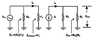
Fig 9 Equivalent CB Amplifier
The above figure shows the diode curve relating IE and VBE. In the absence of ac signal, the transistor operates at Q point (point of intersection of load line and input characteristic). When the ac signal is applied, the emitter current and voltage also change. If the signal is small, the operating point swings sinusoidally about Q point (A to B).
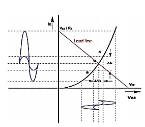
Fig 10 Q-Point
If the ac signal is small, the points A and B are close to Q, and arc A B can be approximated by a straight line and diode appears to be a resistance given by
r’e = 
=  =
= 
If the input signal is small, input voltage and current will be sinusoidal but if the input voltage is large then current will no longer be sinusoidal because of the non-linearity of diode curve. The emitter current is elongated on the positive half cycle and compressed on negative half cycle. Therefore, the output will also be distorted. r'e is the ratio of ΔVBE and Δ IE and its value depends upon the location of Q. Higher up the Q point small will be the value of r' e because the same change in VBE produces large change in IE. The slope of the curve at Q determines the value of r'e. From calculation it can be proved that
r'e = 25mV / IE
Characteristics of Common Base Amplifier
(i) Current gain is less than unity and its magnitude decreases, with the increase of load resistance RL
(ii) Voltage gain AV is high for normal values of RL
(iii) The input resistance Ri is the lowest of all the three configurations, and
(iv) The output resistance Ro is the highest of all the three configurations.
Applications The CB amplifier is not commonly used for amplification purpose. It is used for
(i) Matching a very low impedance source
(ii) As a non-inverting amplifier to voltage gain exceeding unity.
(iii) For driving a high impedance load. (iv)As a constant current source.
Common Collector Amplifier
(i) For low RL (< 10 kΩ), the current gain Ai is high and almost equal to that of a CE amplifier.
(ii) The voltage gain AV is less than unity.
(iii) The input resistance is the highest of all the three configurations.
(iv) The output resistance is the lowest of all the three configurations.
Applications The CC amplifier is widely used as a buffer stage between a high impedance source and a low impedance load.
Key takeaway

Voltage Amplification Factor (Avs) taking into account the resistance (Rs) of the source
This overall voltage gain Avs is given by
Avs = V2 / VS = V2 V1 / V1VS = Av V1/ VS
From the equivalent input circuit using Thevenin’s equivalent for the source shown in Figure
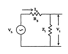
Fig11 Thevenin’s Equivalent
V1 = VS Zi / (Zi + RS)
V1 / VS = Zi / (Zi + RS)
Then, Avs = Av Zi / (Zi + RS)
Substituting Av = Ai ZL / Zi
Avs = Ai ZL / (Zi + RS)
Avs = Ai ZL RS / (Zi + RS) RS
Avs = Ais ZL / RS
Avs = (AI RL/Zi) * (Zi/Rs + ZL) = (AI RL/Rs + Zi)
Effect due to RL
If Rs= 0
Then,
Avs = (AI RL/Zi)
Current Amplification (Ais) taking into account the source Resistance (RS)
The modified input circuit using Norton’s equivalent circuit for the calculation of Ais is shown in Figure.
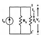
Fig 12 Norton Equivalent
Overall Current Gain,
Ais = -I2 / IS = - I2I1 /I1
IS = Ai I1/IS
From Figure
I1= IS RS / (RS + Zi)
I1 / IS = RS / (RS + Zi)
and hence, Ais = Ai RS / (RS + Zi)
Key takeaway
The current gain becomes
Ais = Ai RS / (RS + Zi)
Effect due to RL
If Rs= 0
Then,
Avs = (AI RL/Zi)
This is also called as common collector amplifier. It is basically used to provide current gain and for impedance matching. The circuit is shown below where the input is applied through base and output is obtained from emitter. The voltage gain is always<1 and output voltage are in phase with input voltage. The output follows the input hence it is called as emitter follower.
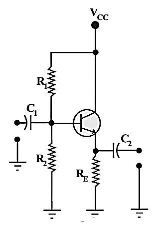
Fig 13 Emitter Follower
The base voltage can be obtained by applying voltage division rule on R2 and R1
VB =  VCC
VCC
The emitter voltage is VE = VB – 0.7
The emitter current is IE = 
VCEQ = VCC-VE
For A.C analysis the circuit can be drawn as shown below
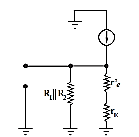
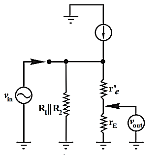
Fig 14 A.C equivalent circuit
The total equivalent ac emitter resistance is rE which is
rE = RE||RL
Practically re’ << rE. The voltage gain then becomes
AV = 1
This relationship is due to the current divisions that occur in both the input and output circuits. we have used in place of hfe. We are assuming that is approximately equal to hfe. The subscript “c” merely indicates that the parameter applies to the emitter follower (common collector) rather than the common emitter amplifier. The exact equation for hfc is
hfc = hfe +1
Since is normally much greater than 1, we normally assume that they are approximately equal.
where:
hfe= transistor current gain
re’= the ac emitter resistance
rE = RL||RE
The output impedance is the impedance that the circuit presents to its load. When a load is connected to the circuit, the output impedance of the circuit acts as the source impedance for that load.
Zout = RE|| [re’ + (Rin’/hfe)]
Key takeaway
The voltage gain is always<1 and output voltage are in phase with input voltage. The output follows the input hence it is called as emitter follower.
A cascade amplifier is a two-port network designed with amplifiers which are connected in series when every amplifier transmits its o/p to the second amplifiers input in a chain. The circuit diagram for two stage amplifiers is shown below.
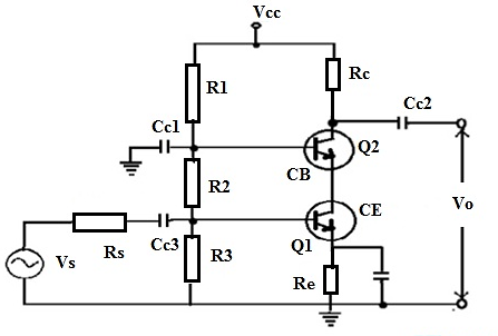
Fig 15 Cascade Amplifier
In order to achieve proper amplification cascade amplifiers are used. The overall gain is Av= Av1 x Av2
The CB configuration provides high frequency operation. The CB and CE configurations are used. The current gain and input resistance are equivalent to related values of CE amplifier. The output can be equivalent to CB configuration. They are used in tuned RF amplifiers. They can also be used as wideband amplifiers.
Darlington Connection
The Darlington pair is a combination of two common collector cascade configuration. In Darlington pair the collectors of the two transistors are connected together, emitter of Q1 is connected to the base of Q2 and emitter of Q2 acts as the emitter of Darlington connection.
The important feature of the Darlington connection is that the composite will act as a single unit, the current gain of which is equal to the product of the individual current gains β1 and β2.
In general Darlington connection with more than 2 transistors is not used because
1) With increase in transistors, leakage current increases.
2) The voltage gain of CC is approximately 1 but that of the Darlington is much less than 1. With increase in transistor, voltage gain will decrease further.
Advantages:
1) Very high current gain.
2) Very low voltage gain.
3) Very high input impendence.
4) Very low output impendence.
Disadvantage – more than 2 transistors cannot be used.
Analysis of Darlington emitter follower –
The circuit diagram of the Darlington emitter follower is shown above.
Assumptions –
1) Both Q1 and Q2 are identical.
2) hoe  0.1 i.e., approximate analysis.
3) hfe RE >> hie
1.Current gain of the Darlington emitter follower (AI):
a) Current gain of Q2:
AI2  = (1 + hfe)
b) Current gain of Q1:
the input resistance of stage 2 acts as the load for Q1
 Ri2 = hie + (1 + hfe) RL2
= hie + AI2RE {where RL2 = RE}
As Ri2 is large, the condition hoe RL’ < 0.1 is not satisfied by first stage
Where RL’ = RL2 = RE
Hence using exact analysis for Q1
 AI1 =
AI1 = 
Substitute  and
and  , we get
 AI1 =
AI1 =  -------------(1)
But  hence, RL1 = Ri2 = hie + hfeRE
Substituting the expression for RL1 in equation (1)
AI1 = 
hoehie is very small so neglecting it,
AI1 = 
Overall current gain: AI = 
i.e., AI = AI1  AI2
AI2
= 
AI -------------(2)
The above equation shows that overall current gain of the Darlington connection is much higher than that of the single emitter follower (common collector).
2.Overall input resistance (Ri):
The overall input resistance will be same as the input resistance of first stage Q1
 Ri = Ri1
Ri1 = hie + AI1RL1 where RL1 = Ri2
Substituting the value of AI1 and Ri2, we get
Ri1 = hie RE --------------(3)
2nd term in equation (3) is much larger than first term, so neglecting hie
Input resistance, Ri1 = RE
RE
If hoehfeRE << 1, then
Ri1 = RE ----------------(4)
For a single CC amplifier Ri = hie +  RE
RE
Equation (4) shows that due to Darlington connection, there is tremendous increase in input resistance.
3.Voltage Gain of Darlington connection (AV):
Overall voltage gain AV = 
AV2 is calculated using approximate analysis.
AV1 is obtained by exact analysis.
a) Voltage gain AV2 = 
AI2 = 1 + hfe
Ri2 = hie + (1 + hfe) RL2
RL2 = RE

{Adding and subtracting hie in numerator}
AV2 = 1  ----------(5)
b) Voltage gain AV1: AV1 = AI1
But for single emitter follower,
AI1 = (1 + hFe),
Ri1 = hie + AI1RL1
AV1 =  where RL1 = Ri2
Adding and subtracting hie in numerator of right-hand side, we get
AV1 = 
AV1 = 1 - 
AV1 = 1 -  -----------(6)
Overall voltage gain = AV = AV1 × AV2
i.e., AV = AV2 = 
AV = 
It is evident that Ri1 >> Ri2 hence 3rd and 4th term in above equation can be neglected
AV = 1 -  -------------(7)
Comparing (5) and (7)
AV  AV2
AV2
The overall voltage gain is approximately equal to the voltage gain of second stage.
4.Overall output resistance RO:
The overall output resistance of the emitter follower Darlington circuit is same as the output resistance of second stage.
YO = hoc 
Hence YO2 = hOC 
Hence YO2 = hOC 
RS for 2nd stage is R01 i.e., output resistance of 1st stage.
But hrc = 1, hOC = hOe, hFC = - (1 + hFe) and hiC = hie
YO2 = hoe + 
Neglect hOe because we are performing approximate analysis for the second stage we get,
YO2 = 
Hence, RO2 = 
But, RO1 = 

RO = RO2 =  +
+ 
Neglect the 2nd term due to  in denominator

The above equation tells us that the RO of Darlington emitter follower is much less than that of a single emitter follower.
Key takeaway
For emitter follower
The value of Z is typically higher than the common emitter amplifier. The voltage gain is always less than 1 The heavy swamping of the circuit virtually eliminates the effect of r’ on the voltage gain.
Que. For T1 hie1 = 6 KΩ hFe1 = 80 hre1 = hoe1 = 0
For T2 hie2 = 1 KΩ hFe2 = 100 hre2 = hoe2 = 0
For the Darlington pair emitter follower, shown in figure, determine:
a) Input impendence R1
b) Voltage gain VO / VS
c) Current gain IO / IS
d) Output impendence
Sol – Given: hie1 = 6 KΩ hFe1 = 80 hre1 = hoe1 = 0
hie2 = 1 KΩ hFe2 = 100 hre2 = hoe2 = 0
Amplifier configuration:
Q1 → CC Q2 → CC
Therefore, approximate analysis is used, for both stages
For second stage:
Current gain (Ai2)
AI2 =  = 1 + 100 = 101
Input resistance (Ri2)
RL1 = Ri2 = hie2 + (1 + hFe2) RL = 1 × 10³ + (1 + 100) × 103 = 102 KΩ
Voltage gain (AV2):
AV2 =  =1 -
=1 -  0.99
0.99
For first stage:
Current gain (Ai1):
Ai1 = 1 + hFe1 = 81
Input resistance (Ri1):
Ri1 = hie1 + (1 + hFe1) RL
= 6 × 10³ + (1 + 80) × 102 × 103 = 8.268 MΩ
Voltage gain (AV1):
AV1 =  = 1 -
= 1 -  0.999
0.999
RO1 =  86.42 Ω
RO2 =  10.76 Ω
Overall voltage gain (AV):
AV = AV1 × AV2 = 0.999 × 0.99 = 0.989
AVS
Figure shows equivalent circuit of the input side
 0.998
0.998
AVS = 0.989 × 0.998 = 0.987
Overall voltage gain:
AI = Ai = Ai1 × Ai2 = 81 × 101 = 8181 Ans.
Input impendence:
Ri = 0.89 MΩ Ans.
Overall voltage gain:
AV = 0.989 Ans.
Voltage gain include source:
AVS = 0.987 Ans.
Output Impendence:
RO = 10.76 Ω Ans.
Que. For the bootstrap circuit shown, calculate AI, Ri and AV. the transistor parameters are hie = 2 KΩ, hFe = 100,  = 40 K and hre = 2.5 × 10⁻⁴.
Sol – Given: hie = 2 KΩ, hFe = 100,  = 40 K, hre = 2.5 × 10⁻⁴.
Amplifier configuration: common emitter with Re
AC analysis: For a.c. analysis of amplifier we consider the d.c. supply voltage as ground and capacitor as short circuit and apply Miller’s theorem across feedback resistor (10K) then modified circuit is given as:
The circuit down in fig. (a) represents a CE amplifier. But to analyse the bootstrapped element we need to consider the CC voltage gain first.
AV =  common collector voltage gain
RL’ = 2K || 4K || 4K ||  1 K || 490 K = 1 KΩ
Assume AV  0.98
0.98
Checking approximation:
hoeRL’  0.1
0.1
0.025 < 0.1
Hence, valid approximation
Approximate analysis:
AI = 1 + hFe = 101
Ri = hie + (1 + hFe) RL’ = 2 + 101 = 103 KΩ Ans.
AV = AI = 0.98
From fig. (a): R1  500 KΩ
Now, fig. (a) can be analysed by CE and the modified circuit is given as,
Checking approximation:
hoe (Re + RL)  0.1
0.1

Hence, valid approximation
Approximate analysis:
AI’=  -hFe = -100
Ri’= hie + (1 + hFe) Re’ = 2 + 101 × 1 = 103 KΩ
AV’ = 
AV = AV’ = -2.9126
From fig. (b): Ri = Ri’ || 500K = 100 || 500 = 85.406 KΩ
AI = 
= (-1) × 100 × 
From fig. (c):  -
-  = 0.8291
Hence, AI = - 100 × 0.82918 = -82.918
Que. The bootstrapped Darlington pair uses identical transistors with the following h-parameters.
hie = 1 KΩ, hre = 2.5 × 10⁻⁴, hoe = 2.5 × 10⁻⁴ A/V, hFe = 100
Find 
Sol - Given: hie = 1 KΩ, hre = 2.5 × 10⁻⁴, hoe = 2.5 × 10⁻⁴ A/V, hFe = 100
Q1 – CC, Q2 - CC
For a.c. analysis of amplifier we consider the d.c. supply voltage as ground and capacitor as short circuit.
Apply Miller’s theorem across R3 = (100K)
Voltage Gain:
AV =  AV1 × AV2
Let us assume AV = 0.98
Where,  = 4900 KΩ
RL’ = 0.1K || 82K || 10K ||  0.1 K || 82 K || 10 K || 4900 K = 0.0988 KΩ
Analysis for Q2 [CC]:
Checking approximation:
hoeRL’ =  0.0988 = 2.47 × 10⁻³ < 0.1
Approximate analysis:
AI2 = 1 + hFe = 101
Ri2 = hie + (1 + hFe) RL’ = 1 + 101 × 0.0988 = 10.9788 KΩ
AV2 = AI2 = 0.908915
Analysis for Q1 [CC]:
RL = Ri2
hoeRL1 =  = 0.27447 > 0.1
Exact analysis:
AI2 =  = 79.2486
Ri1 = hie + AI1hrcRL1 = 1 + 79.2486 × 10.9788
= 871.054 KΩ (hrc  1)
1)
AV1 = 
= 0.99885
AV  AV1 × AV2 = 0.99885 × 0.908915
= 0.9079 (Ans)
Ri = R || Ri1 = 1085.78 || 871.054 {Fig. (a)}
= 483.32 KΩ
 AI1 = 79.2486
AI = 
= 


AI = (-0.9889) × (-101) × (-1) × (-79.2486) × 0.55487
= 4391.94 (Ans)
Equation for VO/Vi:
Analysis of Q2 [CC]:
hoe (Re+RL)
 × [0.0988 + 1] = 0.02747 < 0.1
Approximate analysis
AI2 = - hFe = -100
Ri2 = hie + (1 + hFe) Re
= 1 +(1 + 100)0.0988 = 10.9788 KΩ
AV2 =  =
=  -9.1084
Analysis of Q1 [CC]:
RL1 = Ri2 = 10.9788 KΩ
hoeRL1 =  = 0.27447 > 0.1
Exact analysis:
AI1 =  = 79.2486
RL1 = hie + AI1RL1 = 1 + 79.2486 × 10.9788
= 871.054 KΩ
AV1 =  =
= 
 AV = AV1 × AV2 = -9.0975
Hence, -AI1 =  79.248

Ri = 483.32 KΩ
 -9.0975 (Ans)
Que. A bootstrapped Darlington amplifier shown in fig. uses identical transistor with h-parameters, hie = 1.5 KΩ, hoe = 50 μA/V. If the circuit is to have Ri of 268 MΩ. Find the value of hFe for the transistor used.
Sol – Given: hie = 1.5 KΩ, hoe = 50 μA/V, Ri = 2.68 MΩ, R1 = 1 MΩ, R2 = 1 MΩ, Re2 = 1 KΩ
RLeft = RC1 || RC2 = ∞ || 1 K = 1 KΩ
Amplifier configuration: bootstrapped Darlington pair amplifier [CC - CC]
Checking for approximation:
hoeRLeft  0.1
0.1
hoeRLeft = 25 × 10-6 × 1 K = 0.025 < 0.1
which is less than 0.1
Approximate analysis:
Calculation for hFe
Ai2 = 1 + hFe
Ri2 = hie2 + Ai2RLeft = 1.5 K + (1 + hFe)1 K
Ai1= 1 + hFe
Ri1 = hie1 + Ai1RL1
Where RL1 = Ri2
Ri1 = 1.5K + (1 + hFe) [1.5K + (1 + hFe)1K]
2.68 MΩ = 1.5K + 1.5K + (1 + hFe)1K + 1.5Khfe + (1+hFe) 1KhFe
= 3K + 1K + 1KhFe + 1.5KhFe + 1KhFe + 1KhFe2
= 4K + 3.5KhFe + 1KhFe2
= (4 + 3.5hFe + hFe2) × 103
 hFe2 + 3.5hFe + 4 = 2680
 hFe2 + 3.5hFe - 2676 = 0
The quadratic equation can be solved as,
hFe = 
Substituting values we get,
hFe 
=  50 or -53.5
hFe is always positive.
 hFe = 50 Ans.
Overall voltage gain:
(AV): AV = AV1 × AV2 = (1 -  )( 1 -
  )
)
= (1 -  )( 1 -
  )
)
= 0.999 × 0.971 = 0.97
Overall current gain –
Ai = Ai1 × Ai2
= (1 + hFe) (1 + hFe)
= (51)(51)
= 26.01
Current Mirror Circuits
Here at the Q2 side, more current mirrors need to be used to provide current KID2=KID1. Also, it can be seen that all internal nodes have low impedance except the output node. By using proper current mirrors with high output impedance, good gain can be achieved. The overall transfer function of this Op-Amp closely approximate dominant-pole operation.
Av =  =
=  =
= 


Unity-gain frequency  =
=  =
= 
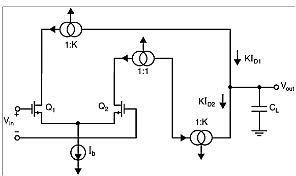
Fig 16 Current Mirror Circuit
If power dissipation is specified, then total current is given by,

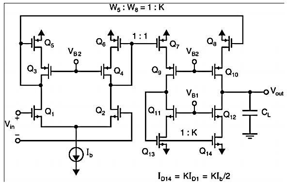
Fig 16 Circuit for Current Mirror
It can be seen that larger K increases the unity-gain frequency assuming the load capacitor dominates the time constants. Larger K also increases the gain. A typical upper limit for K is 5. A detailed analysis reveals important nodes for determining the non-dominant poles, at the drain of Q1 first and drain of Q2 and Q9 secondly.
Larger K increases the capacitances at these nodes while also increases the resistance (assuming a fixed Itotal), which reduce the non-dominant poles. In this case, then CL has to be increased to maintain a large phase margin.
So, K should not be too large, i.e., K<=2 usually. During slew rate, all of the bias current Ib of the first stage is diverted through Q1/2 and amplified by the current mirror gain to the output. The total current to charge/discharge the load is KIb.
So, the slew rate is Due primarily to the larger unity-gain frequency and slew rate, the current-mirror OpAmp may be preferred over the folded-cascade OpAmp.
However, one has to be careful that the current-mirror OpAmp has larger input noise as well, as its input stage is biased at a lower portion of the total bias current and therefore a relatively smaller gm given the same power consumption.
Key takeaway
Sr. No. | Parameter | Expression |
1 | Current gain (AI) | AI |
2 | Input resistance (Ri) | Ri = |
3 | Voltage gain (AV) | AV = 1 - |
4 | Output resistance (RO) | RO = |
Field Effect Transistor (FET) amplifiers provide an excellent voltage gain and high input impedance. Because of high input impedance and other characteristics of JFETs they are preferred over BJTs for certain types of applications.
There are 3 basic FET circuit configurations
i) Common Source
ii) Common Drain
iii) Common Gain
Similar to BJT CE, CC and CB circuits, only difference is in BJT large output collector current is controlled by small input base current whereas FET controls output current by means of small input voltage. In both the cases output current is controlled variable. FET amplifier circuits use voltage-controlled nature of the JFET. In Pinch off region, ID depends only on VGS.
The linear small signal equivalent circuit for the FET can be obtained in a manner similar to that used to derive the corresponding model for a transistor. We can express the drain current iD as a function f of the gate voltage and drain voltage Vds.
Id = f(Vgm, Vrd) (1)
The transconductance gm and drain resistance rd: - If both gate voltage and drain voltage are varied, the change in the drain current is approximated by using Taylor’s series considering only the first two terms in the expansion


Where 

Is the mutual conductance or trans-conductance. It is also called as gfs or yfs common source forward conductance. The second parameter rd is the drain resistance or output resistance is defined as
rd =  gs
gs 
 Vgs =
Vgs =  |vgs
|vgs
rd =  |vgs
|vgs
The reciprocal of the rd is the drain conductance gd. It is also designated by Yos and Gos and called the common source output conductance. So, the small signal equivalent circuit for FET can be drawn in two different ways.
1.small signal current –source model
2.small signal voltage-source model.
A small signal current –source model for FET in common source configuration can be drawn satisfying Equation (1). This low frequency model for FET has a Norton’s output circuit with a dependent current generator whose magnitude is proportional to the gate-to –source voltage.
The proportionality factor is the transconductance ‘gm’. The output resistance is ‘rd’. The input resistance between the gate and source is infinite, since it is assumed that the reverse biased gate draws no current. For the same reason the resistance between gate and drain is assumed to be infinite. The below section covers the detailed analysis.
Common Source (CS) Amplifier

Fig 17 CS Amplifier and Small Signal equivalent Circuit
A simple Common Source amplifier and associated small signal equivalent circuit using voltage-source model of FET is shown in Figure above.
Voltage Gain
Source resistance (RS) is used to set the Q-Point but is bypassed by CS for mid-frequency operation. From the small signal equivalent circuit, the output voltage
VO = -RDµ Vgs (RD + rd)
Where Vgs = Vi,
the input voltage,
Hence, the voltage gain,
AV = VO / Vi = -RDµ (RD + rd)
Input Impedance
Zi = RG
For voltage divider bias as in CE Amplifiers of BJT
RG = R1 ║ R2
Output Impedance
Output impedance is the impedance measured at the output terminals with the input voltage VI = 0. When the input voltage Vi = 0, Vgs = 0
and hence µ Vgs = 0
The equivalent circuit for calculating output impedance is given in Figure below.
Output impedance
Zo = rd ║ RD
Normally rd will be far greater than RD. Hence Zo ≈ RD
Common Drain Amplifier
A simple common drain amplifier is shown in Figure above and associated small signal equivalent circuit using the voltage source model of FET. Since, voltage Vgd is more easily determined than Vgs, the voltage source in the output circuit is expressed in terms of Vgs and Thevenin’s theorem.

Fig 18 CD Amplifier and Small Signal equivalent circuit
Voltage Gain
The output voltage, VO = RS µVgd / (µ + 1) RS + rd
Where Vgd = Vi the input voltage.
Hence, the voltage gain,
Av = VO / Vi = RS µ / (µ + 1) RS + rd
Input Impedance
From Figure above,
Input Impedance
Zi = RG
Output Impedance
From above figure,
Output impedance measured at the output terminals with input voltage Vi = 0 can be calculated from the following equivalent circuit.
As Vi = 0: Vgd = 0: µ vgd / (µ + 1) = 0
Output Impedance ZO = rd / (µ + 1) ║RS
When µ » 1
ZO = ( rd / µ) ║RS = (1/gm) ║RS
Common Gate Amplifier
In common source amplifier and source follower circuits, the input signal is applied to the gate of a MOSFET. It is also possible to apply the input signal to the source terminal by keeping common gate terminal. This type of amplifier is called as common gate amplifier.
Figure below shows the CG amplifier in which the input signal is sensed at the source terminal and the output is produced at the drain terminal. The gate terminal is connected to VB i.e., dc potential which will maintain the proper operating conditions.

Fig 19 CG Amplifier and Small Signal equivalent circuit
By analysing the small signal equivalent circuit, the voltage gain of CG amplifier is given by,
Av = = gm RD
The important point is the gain is positive, further the input impedance is given by which shows that the input impedance of common gate amplifier is relatively low. Furthermore, the input impedance of gate stage is relatively low only if the load resistance connected to the drain is small.
Key takeaway
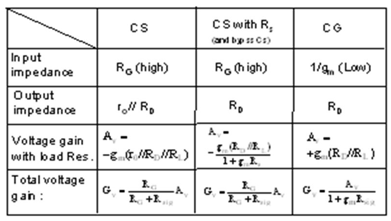
1. The input resistance Rin is infinite.
2. The open-circuit voltage gain, Avo, is reduced by a factor of 1 + gmRs
3. For the same nonlinear distortion, the input signal can be increased by a factor of 1 + gmRs compared to without Rs.
4. As shall be shown later, the high-frequency response of this design is improved.
In general, the addition of the source resistance Rs gives rise to a “negative” feedback factor 1 + gmRs that reduces voltage gain, but improves linearity, and high-frequency response. Because of the negative-feedback action of Rs, it is also called the source-degenerate resistance.
This is similar to the emitter follower for the BJT, which is used as a voltage buffer. It is a unit-gain amplifier with a very large input impedance but a smaller output impedance. Therefore, it is good for matching a high-impedance circuit to a low-impedance circuit or to a circuit that needs a larger supply of current.
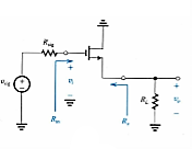
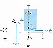
Fig 20 CD Source Follower and it’s equivalent circuit
Characteristics of a Source Follower
The small-signal circuit and a T-model equivalent circuit diagram for a source follower. The input source is represented by a Thevenin equivalent voltage vsig and resistor Rsig. A load resistor is connected to the output between the source and ground.
Since the gate current is zero for this circuit,
Rin = ∞
Using the voltage divider formula, it is seen that voltage gain proper or terminal voltage gain is
Av = vo/vi = RL/ (RL + 1/gm)
For the open-circuit voltage gain, RL = ∞ and Avo = 1
The output resistance is obtained by replacing the proper part of the amplifier with a Thevenin equivalence. To this end, with the use of the test-current method, one sets the value of vi = 0, and thus Ro = 1/gm
Because of the infinite input impedance Rin, then vi = vsig, and the overall voltage gain Gv (also called the total voltage gain) is the same as the voltage gain proper Av (also called terminal voltage gain) Gv = Av = RL/ (RL + 1/gm)
Since 1/gm is typically small, with large RL, the gain is less than unity, but is close to unity. Hence, this is a source follower, because the source voltage follows the input voltage, but yet, it can provide a larger current to the output than the input current.
Cascade Amplifier
Cascade of Self Biased FET
Zi = RG1
Zo =RD2 || rd
Z01 = RD1 || rd || RG2 = RD
AV = AV1 * AV2
= -gm (RD1 || rd) * -gm (RD2|| rd)
=gm2 (RD1 || rd) * (RD2|| rd)
References:
1. Microelectronics Circuits, Adel Sedra and Kenneth C Smith, Oxford University Press, New Delhi, 5th Edition, International Student Edition,2009. (Selected portion of Chapter 2,4, 5, 6, 8, 13, and 14)
2. Electronic Devices and Circuits theory, R.L. Boylestad and L. Nashelsky, Pearson Education, New Delhi, 9th/10th Edition,2013. (Selected portions of Chapter 4, 5, 6, 7, 8, 9, 10, 11, 12, and 14)
3. Milliman’s Electronics Devices and Circuits, J. Milliman, C. Halkias, S. Jit., Tata McGraw Hill


