Unit - 1
MOS Field-Effect Transistor

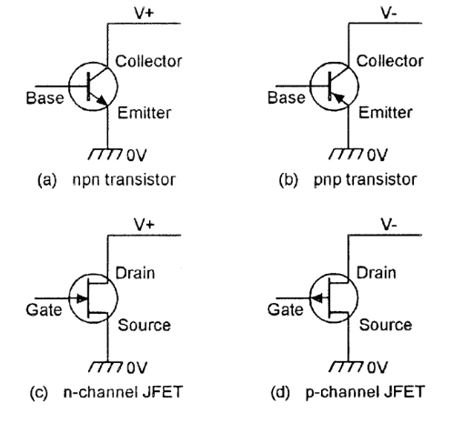
Fig 1 BJT and FET
Operation

I-V characteristics
Output Characteristics or Drain Characteristics
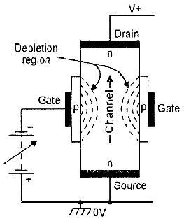
Fig 2 Drain characteristics
2. With external bias: When the external bias is applied to the gate-source terminal, the gate-source terminal becomes reversed bias externally. Obviously, if we are supplying an external voltage, then we can achieve the pinch-off point quite early as compared to the circuit which is not biased.
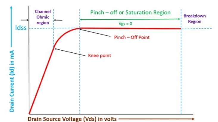
Fig 3 I-V characteristics
Transfer Characteristics
The transfer characteristics can be determined by observing different values of drain current with variation in gate-source voltage provided that the drain-source voltage should be constant. The transfer characteristics are just opposite to drain characteristics.
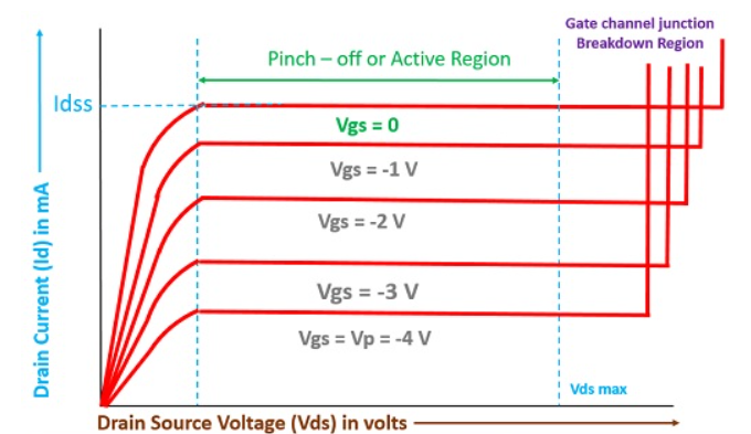
Fig 3 Transfer Characteristics
MOSFETs- types, Operations and their Characteristics
Operation
The MOSFET works by electronically varying the width of a channel along which charge carrier flow (electrons or holes).
The charge carriers enter the channel through source and exit via the drain. The width of the channel is controlled by the gate voltage which is located between source and drain. It is insulated from the channel near an extremely thin layer of metal oxide.
Function:
When there is no voltage on the gate, the channel shows maximum conductance. When the voltage on the gate is either positive or negative, the channel conductivity decreases.
2. Enhancement Mode
The device does not conduct when there is no voltage on the gate. As the voltage increases on the gate, the better the device can conduct.

Fig 4 N-channel and p-channel MOSFET
Working:

Key takeaway
N-Channel MOSFET
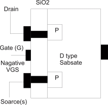
Fig 5 N-channel MOSFET
Effect of the insulting sio2 layer:
Due to the presence of the sio2 layer between gate terminal and n-type channel the i/p impedance of MOSFET is very high this is a desirable fracture of a MOSFET. Due to high i/p impedance the gate current IG= 0 for the d.c operating conditions.
Operation: The operation can be explained with two different operating
1) Operating with VGS = 0 Volt
If VGS = 0 and a positive voltage is applied between its drain and source then due to the absence of the n-type channel a zero-drain current will result.
2) Operation when Vgs Positive:
The positive potential at the gate terminal will repel the holes present in the p-type substrate.
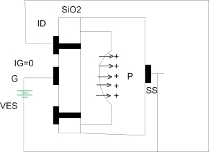
Fig 6 N-channel MOSFET for Vgs positive
Formation of induced channel in n-channel enhancement MOSFET
This creates a depletion region near the sio2 insulating layer. But the minority carriers i.e., the electrons in the p-type substrate will be attracted towards the gate terminal and gather near the surface of sio2 as shown above
As we increase the positive VGS the number of e- gathering near the sio2 layer increases to such an extent that it creates an induced n-channel which connects the n-type doped regions.
The drain current then starts flowing through this induced channel. The value of VGS at which this conduction begins is called as the threshold Vtg. & is indicated.
Characteristics of n-channel enhancement type MOSFET:
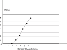
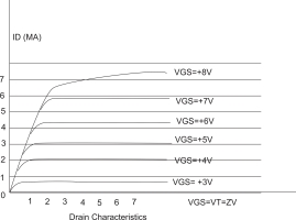
Fig 7 Characteristics of N-channel MOSFET
P-channel enhancement type MOSFETS:
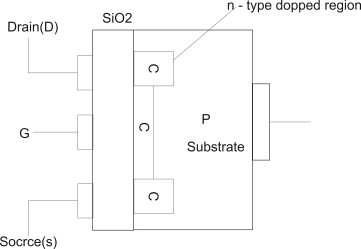
Fig 8 P-channel MOSFET
The construction of p-channel EMOSFET is exactly opposite to that of a n-channel EMOSFET
Characteristics:
Drain Characteristics of transfer Characteristics of p-channel E MOSFET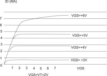
Fig 8 Drain characteristics of P-channel MOSFET
Key takeaway
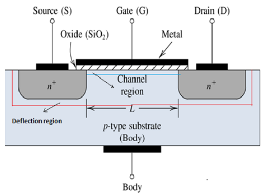
NMOS
NMOS is built on a p-type substrate with n-type source and drain diffused on it. Here, the majority carriers are electrons. When a high voltage is applied to the gate, the NMOS conducts and when low voltage is applied to the gate, it does not conduct. NMOS is faster than PMOS, as the carriers are electrons that travel twice as fast as the holes.
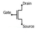
PMOS
P-MOS consists of P-type Source and Drain diffused on an N-type substrate. Here, majority carriers are holes. When a high voltage is applied to the gate, the PMOS does not conduct and when a low voltage is applied, it conducts. These devices are more immune to noise than NMOS devices.
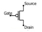
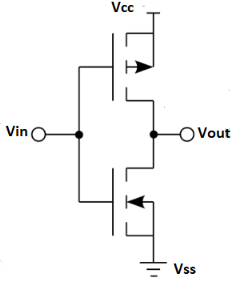
Fig 9 CMOS
The inverter circuit as shown in the figure above. It consists of PMOS and NMOS FET. The input A serves as the gate voltage for both transistors.
The NMOS transistor has an input from Vss (ground) and PMOS transistor has an input from Vdd. The terminal Y is output. When a high voltage (~ Vdd) is given at input terminal (A) of the inverter, the PMOS becomes open circuit and NMOS switched OFF so the output will be pulled down to Vss.
When a low-level voltage (<Vdd, ~0v) applied to the inverter, the NMOS switched OFF and PMOS switched ON. So, the output becomes Vdd or the circuit is pulled up to Vdd.
INPUT | LOGIC INPUT | OUTPUT | LOGIC OUTPUT |
0 V | 0 | Vdd | 1 |
Vdd | 1 | 0 v | 0 |
Key takeaway
The V-I characteristics of the depletion-mode MOSFET transistor are drawn between the drain-source voltage (VDS) and drain current (ID). The small amount of voltage at the gate terminal will control the current flow through the channel. The channel formed between the drain and the source will act as a good conductor with zero bias voltage at the gate terminal. The channel width and drain current will increase if the positive voltage is applied to the gate whereas they will get decreased when we apply a negative voltage to the gate.
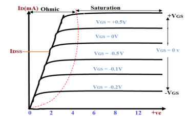
Fig 10 V-I Characteristics of DMOSFET
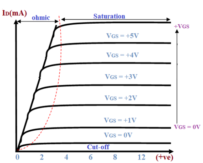
VI characteristics of the enhancement-mode MOSFET are drawn between the drain current (ID) and the drain-source voltage (VDS). The VI characteristics are partitioned into three different regions, namely ohmic, saturation, and cut-off regions. The cut-off region is the region where the MOSFET will be in the OFF state where the applied bias voltage is zero. When the bias voltage is applied, the MOSFET slowly moves towards conduction mode, and the slow increase in conductivity takes place in the ohmic region. Finally, the saturation region is where the positive voltage is applied constantly and the MOSFET will be staying in the conduction state.

Fig 11 V-I Characteristics of EMOSFET
Key takeaway
BJT | FET | MOSFET | |
Device type | Current controlled | Voltage controlled | Voltage Controlled |
Current flow | Bipolar | Unipolar | Unipolar |
Terminals | Not interchangeable | Interchangeable | Interchangeable |
Operational modes | No modes | Depletion mode only | Both Enhancement and Depletion modes |
Input impedance | Low | High | Very high |
Output resistance | Moderate | Moderate | Low |
Operational speed | Low | Moderate | High |
Noise | High | Low | Low |
Thermal stability | Low | Better | High |
MOSFET as an Amplifier
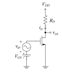
Figure.12 MOSFET as as Amplifier
This is a conceptual amplifier for two resons:
To operate as small -signal amplifier we bias MOSFET in saturation region. For analysis of DC operating point we set vgs =0 so that
iD = ½ Kn’ W/L (vgs -Vt) 2 --------------------(1)
From the circuit VDS = VDD – ID RD ------------------------------(2)
For operation in saturation region
vGD ≤ Vt ------ vgs – vds ≤ Vt
or vds ≥ vgs – Vt --------------------------------------------------(3)
where the total drain to source voltage is
vds = Vds + vds
(bias) AC
With an AC signal applied at the gate
Vgs = VGS + vgs -------------------------------(4)
Substituting (4) in (1) we get
iD = ½ kn’ W/L (VGS + vgs – Vt) 2 = ½ kn’ W/L (VGS – Vt) + vgs ] 2 ----------(5)
= ½ kn’ W/L (VGS – Vt) 2 + 2/2 kn ‘ W/L (VGS – Vt) vgs + ½ kn’ W/L v 2 gs ---------(6)
The last term is non linear in vgs which is not desorable for linear amplifier. Hence for linear operation the last term should be small with respect to linear term and the second term is proportional to vgs.
Or vgs<< 2 (VGS – Vt) ------------------------------------------(7)
If this small signal condition (7) is satisfied then from (6) the total drain current is a approximately linear summation.
iD ͌ ID + i d --------------------------------------------------------------(8)
where
id = kn’ W/L (VGS – Vt) vgs ‘ ---------------------------------------(9)
From this expression (9) we see that AC drain current id is related to vgs by transistor transconductance gm.
gm = id / vgs = kn’ W/L (VGS – Vt) [S]
which is sometimes expressed in terms of overdrive voltage VoV = Vgs – Vt
gm = kn’ W/L Vov [S]
MOSFET as a switch
The drain terminal (D) of the MOSFET is connected to the supply voltage VS via the drain resistor RD while its source terminal (S) is grounded. It has an input voltage Vi applied at its gate terminal (G) while the output Vo is drawn from its drain.
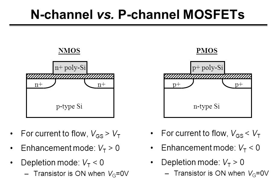
Figure.13 n-channel Enhancement MOSFET functioning as a switch
When Vi > VT under this condition, the MOSFET will start to conduct and if the VS provided is greater than the pinch-off voltage VP of the device then the MOSFET starts to operate in its saturation region.
Thus, the output voltage alters between VS and zero depending on whether the input provided is less than or greater than VT, respectively. Thus, it can be concluded that MOSFET can be made to function as electronic switches when made to operate between cut-off and saturation operating regions.
Key takeaway
MOSFET as a switch
The drain terminal (D) of the MOSFET is connected to the supply voltage VS via the drain resistor RD while its source terminal (S) is grounded. It has an input voltage Vi applied at its gate terminal (G) while the output Vo is drawn from its drain.
Load line Analysis

Fig.14: DC Load Line (Ref. 2)


Fig.15: DC Load Line characteristic curve (Ref. 2)

AC Load Line
The DC load line discussed previously, analyses the variation of collector currents and voltages, when no AC voltage is applied. Whereas the AC load line gives the peak-to-peak voltage, or the maximum possible output swing for a given amplifier.
We shall consider an AC equivalent circuit of a CE amplifier for our understanding.
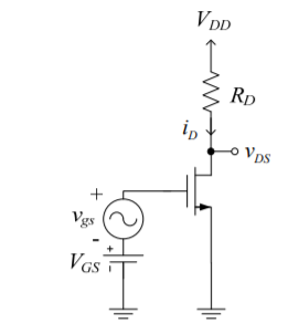
Fig 16 AC Load Line
VCE = (RC||R1) x IC
rC = RC || R1
For a transistor to operate as an amplifier, it should stay in active region. The quiescent point is so chosen in such a way that the maximum input signal excursion is symmetrical on both negative and positive half cycles.
Hence,
Vmax=VCEQ and Vmin = −VCEQ
The following graph represents the AC load line which is drawn between saturation and cut off points.
the current IC at the saturation point is
IC (sat)=ICQ+(VCEQ/rC)
The voltage VCE at the cut-off point is
VCE (off)=VCEQ+ICQ rC
Hence the maximum current for that corresponding
VCEQ = VCEQ / (RC ||R1) is
ICQ=ICQ∗(RC||R1)
Hence by adding quiescent currents the end points of AC load line are
IC (sat)=ICQ+VCEQ/(RC||R1)
VCE (off)=VCEQ+ICQ∗(RC||R1)
When AC and DC Load lines are represented in a graph, it can be understood that they are not identical. Both of these lines intersect at the Q-point or quiescent point. The endpoints of AC load line are saturation and cut off points. This is understood from the figure below.

Fig17 AC and DC Load Line
From the above figure, it is understood that the quiescent point (the dark dot) is obtained when the value of base current IB is 10mA. This is the point where both the AC and DC load lines intersect.
Key takeaway
In DC load line the variation of collector currents and voltages, when no AC voltage is applied. Whereas the AC load line gives the peak-to-peak voltage, or the maximum possible output swing for a given amplifier.
Numerical
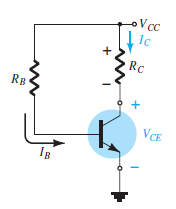
Determine the values of VCC RC and RB of a fixed bias configuration for a given load line and defined Q point.
Solution:

When a line is drawn joining the saturation and cut off points, such a line can be called as Load line. This line, when drawn over the output characteristic curve, makes contact at a point called as Operating point.
This operating point is also called as quiescent point or simply Q-point. There can be many such intersecting points, but the Q-point is selected in such a way that irrespective of AC signal swing, the transistor remains in the active region.
The following graph shows how to represent the operating point.
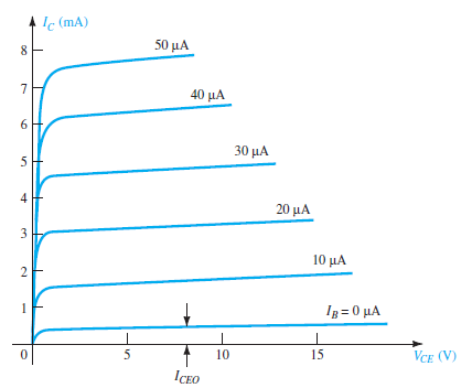
Fig18 Operating Point
The process of increasing the signal strength is called as Amplification. This amplification when done without any loss in the components of the signal, is called as Faithful amplification.
Faithful amplification is the process of obtaining complete portions of input signal by increasing the signal strength. This is done when AC signal is applied at its input.

Fig 19 Amplification with AC input Signal
In the above graph, the input signal applied is completely amplified and reproduced without any losses. This can be understood as Faithful Amplification.
The operating point is so chosen such that it lies in the active region and it helps in the reproduction of complete signal without any loss.
If the operating point is considered near saturation point, then the amplification will be as under.

Fig 20 Operating point near saturation point
If the operation point is considered near cut off point, then the amplification will be as under.

Fig 21 Operating point near cut-off point
Hence the placement of operating point is an important factor to achieve faithful amplification. But for the transistor to function properly as an amplifier, its input circuit (i.e., the base-emitter junction) remains forward biased and its output circuit (i.e., collector-base junction) remains reverse biased.
Key takeaway
To ensure faithful amplification, the following basic conditions must be satisfied.
Fixed Bias
The transistors base current, IB remains constant for given values of Vcc, and therefore the transistors operating point must also remain fixed. Hence, referred as fixed biasing. This two-resistor biasing network is used to establish the initial operating region of the transistor using a fixed current bias.
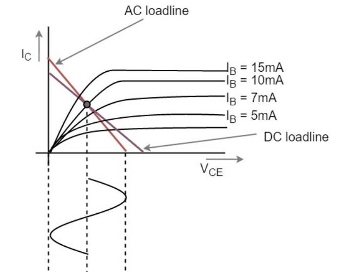
Fig 23 Fixed Bias
VC = VCC -RC (IC +IB)
VE = 0
VB =VBE
IB = VC -VB/RB
IC = β IB
IE = (IC + IE)  IC
IC
This type of transistor biasing arrangement is also beta dependent biasing as the steady-state condition of operation is a function of the transistor beta β value
Self-Bias
This type of transistor biasing configuration, often called self-emitter biasing, uses both emitter and base-collector feedback to stabilize the collector current even further. This is because resistors RB1 and RE as well as the base-emitter junction of the transistor are all effectively connected in series with the supply voltage, VCC.
The downside of this emitter feedback configuration is that it reduces the output gain due to the base resistor connection. The collector voltage determines the current flowing through the feedback resistor, RB1 producing what is called degenerative feedback.
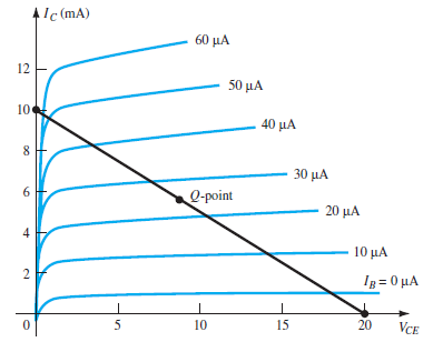
Fig24 Self Biasing of Transistor
VC= VCC- RC (IC + IB1)
VE = IERE = VB – VBE
VCE =VC – VE
VB = VBE + VE
IRB2 = VB/RB2
IRB1 = IB + IRB2 = VC – VB/RB1
IC =  IB
IB
IE = (IC + IB)  IC
IC
The current flowing from the emitter, IE (which is a combination of IC + IB) causes a voltage drop to appear across RE in such a direction, that it reverse biases the base-emitter junction.
So, if the emitter current increases, due to an increase in collector current, voltage drop I*RE also increases. Since the polarity of this voltage reverse biases the base-emitter junction, IB automatically decrease. Therefore, the emitter current increase less than it would have done had there been no self-biasing resistor.
Key takeaway
A transistors steady state of operation depends a great deal on its base current, collector voltage, and collector current and therefore, if a transistor is to operate as a linear amplifier, it must be properly biased to have a suitable operating point. Establishing the correct operating point requires the proper selection of bias resistors and load resistors to provide the appropriate input current and collector voltage conditions.
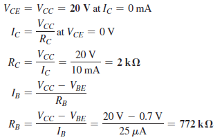
Fig 25 DC Bias with Voltage Feedback
Input Loop
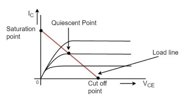
Fig 26 Input Loop
Applying KVL for Input Loop:
VCC = IC1RC + IBRB + VBE + IERE
IC1 - IC and IC
  IE
IE
Substituting for IE as (β +1) IB and solving for IB,
IB = (VCC – VBE) / [ RB + β (RC + RE)]
Output loop
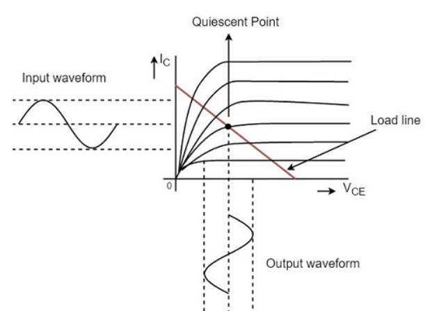
Fig 27 Output Loop
Neglecting the base current, KVL to the output loop results in,
VCE = VCC – IC (RC + RE)
Key takeaway
In this circuit, improved stability is obtained by introducing a feedback path from collector to base. Sensitivity of Q point to changes in beta or temperature variations is normally less than that encountered for the fixed bias or emitter biased configurations.
The process of making the operating point independent of temperature changes or variations in transistor parameters is known as Stabilization.
Once the stabilization is achieved, the values of IC and VCE become independent of temperature variations or replacement of transistor. A good biasing circuit helps in the stabilization of operating point.
Stabilization of the operating point has to be achieved due to the following reasons.
Let us understand these concepts in detail.
Temperature Dependence of IC
As the expression for collector current IC is
IC=βIB+ICEO
=βIB+(β+1) ICBO
The collector leakage current ICBO is greatly influenced by temperature variations. To come out of this, the biasing conditions are set so that zero signal collector current IC = 1 mA. Therefore, the operating point needs to be stabilized i.e., it is necessary to keep IC constant.
Individual Variations
As the value of β and the value of VBE are not same for every transistor, whenever a transistor is replaced, the operating point tends to change. Hence it is necessary to stabilize the operating point.
Thermal Runaway
As the expression for collector current IC is
IC=βIB+ICEO
=βIB+(β+1) ICBO
The flow of collector current and also the collector leakage current causes heat dissipation. If the operating point is not stabilized, there occurs a cumulative effect which increases this heat dissipation. The self-destruction of such an unstabilized transistor is known as Thermal run away. In order to avoid thermal runaway and the destruction of transistor, it is necessary to stabilize the operating point, i.e., to keep IC constant.
Stability Factor
By definition, the rate of change of collector current IC with respect to the collector leakage current ICO at constant β and IB is called Stability factor.
S=dIC/dICOS at constant IB and β
Hence, we can understand that any change in collector leakage current changes the collector current to a great extent. The stability factor should be as low as possible so that the collector current doesn’t get affected. S=1 is the ideal value.
The general expression of stability factor for a CE configuration can be obtained as under.
IC=βIB+(β+1) ICO
Differentiating above expression with respect to IC, we get
1=βdIB/dIC+(β+1) dICO/dIC
Or
1=βdIB/dIC+(β+1)/S
Since dICO/dIC=1/S
Or
S=β+1/[1−β(dIB/dIC)]
Hence the stability factor S depends on β, IB and IC.
Key takeaway
Stabilization of the operating point has to be achieved due to the following reasons.
Q1. A npn silicon transistor has VCC = 6 V and the collector load RC = 2.5 kΩ. Find: (i) The maximum collector current that can be allowed during the application of signal for faithful amplification. (ii) The minimum zero signal collector current required.
Solution:

Collector supply voltage, VCC = 6 V
Collector load, RC = 2.5 kΩ
(i) We know that for faithful amplification, VCE should not be less than 1V for silicon transistor.
∴ Max. voltage allowed across RC = 6 − 1 = 5 V
∴ Max. allowed collector current = 5 V/RC = 5 V/2.5 kΩ = 2 mA
Thus, the maximum collector current allowed during any part of the signal is 2 mA. If the collector current is allowed to rise above this value, VCE will fall below 1 V. Consequently, value of β will fall, resulting in unfaithful amplification.
(ii) During the negative peak of the signal, collector current can at the most be allowed to become zero. As the negative and positive half cycles of the signal are equal, therefore, the change in collector current due to these will also be equal but in opposite direction.
∴ Minimum zero signal collector current required = 2 mA/2 = 1 mA
During the positive peak of the signal [point A in Fig. 1(ii)], iC = 1 + 1 = 2mA
And during the negative peak (point B), iC = 1 − 1 = 0 mA
Q2. A transistor employs a 4 kΩ load and VCC = 13V. What is the maximum input signal if β = 100? Given Vknee = 1V and a change of 1V in VBE causes a change of 5mA in collector current.
Solution:
Collector supply voltage, VCC = 13 V
Knee voltage, Vknee = 1 V
Collector load, RC = 4 kΩ
∴ Max. allowed voltage across RC = 13 − 1 = 12 V
∴ Max. allowed collector current, iC =12 V /RC = 12 V/ 4 KΩ = 3 mA
Maximum base current, iB = iC / β = 3 mA / 100 = 30 μA
Now collector-current / Base voltage (signal voltage) = 5 mA/V
∴Base voltage (signal voltage) = Collector current / (5 mA/V) = 3 mA / (5 mA/V) = 600 mV
Q3. Fig. 2 (i) shows biasing with base resistor method. (i) Determine the collector current IC and collector-emitter voltage VCE. Neglect small base-emitter voltage. Given that β = 50. (ii) If RB in this circuit is changed to 50 kΩ, find the new operating point.
Solution:
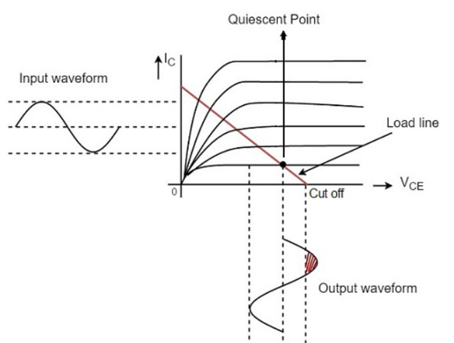
Fig.
In the circuit shown in Fig. 2 (i), biasing is provided by a battery VBB (= 2V) in the base circuit which is separate from the battery VCC (= 9V) used in the output circuit.
The same circuit is shown in a simplified way in Fig. 2 (ii). Here, we need show only the supply voltages, + 2V and +9V. It may be noted that negative terminals of the power supplies are grounded to get a complete path of current.
IB RB + VBE = 2
IB = 20 A
A
IC =  IB = 50x20
 A= 1mA
IC RC + VCE = 9
VCE = 9- (1mA x 2000) = 7V
When RB is made equal to 50k
IC =  IB = 50x40
 A= 2mA
VCE = 9- (2mA x 2000) = 5V
So, the operating point is 5V and 2mA
Q4. Fig. 3 (i) shows that a silicon transistor with β = 100 is biased by base resistor method. Draw the d.c. load line and determine the operating point. What is the stability factor?
Solution:
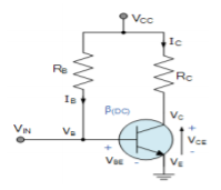
Fig.
Here, VCC = 6 V, RB = 530 kΩ, RC = 2 kΩ
D.C. load line
Referring to Fig. 3 (i), VCE = VCC − ICRC
When IC = 0,
VCE = VCC = 6 V. This locates the first point B (OB = 6V) of the load line on collector-emitter voltage axis as shown in Fig. 3 (ii).
When VCE = 0,
IC = VCC/RC = 6V/2 kΩ = 3 mA.
This locates the second point A (OA = 3mA) of the load line on the collector current axis. By joining points A and B, d.c. load line AB is constructed as shown in Fig. 3(ii).
Operating point Q
As it is a silicon transistor, therefore, VBE = 0.7V.
IB RB +VBE =VCC
IB = (6-0.7)/530x103 =10 A
A
IC =  IB = 100x10= 1mA
VCE = 6- (1mA x 2000) = 4V
The operating point is 4V, 1mA.
The stability factor is given by  +1 = 100+1 =101
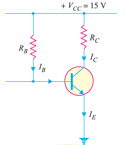
Q5. Design base resistor bias circuit for a CE amplifier such that operating point is VCE = 8V and IC = 2 mA. You are supplied with a fixed 15V d.c. supply and a silicon transistor with β = 100. Take base-emitter voltage VBE = 0.6V. Calculate also the value of load resistance that would be employed.
Solution:
Fig. shows CE amplifier using base resistor method of biasing.
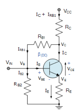
Fig.
Solution:
VCC = 15v
β = 100
VBE = 0.6V
VCE = 8V, IC = 2 mA.
VCC = VCE + IC RC
15 = 8+ 2mAxRC
RC = 3.5k
IC =  IB
IB
IB = 2/100 =0.02mA
VCC = IB RB + VBE
RB = (15-0.6)/ (0.02x10⁻³) = 720k
Q6. In base bias method, how Q-point is affected by changes in VBE and ICBO.
Solution:
In addition to being affected by change in β, the Q-point is also affected by changes in VBE and ICBO in the base bias method.
(i) Effect of VBE:
The base-emitter-voltage VBE decreases with the increase in temperature (and vice-versa). The expression for IB in base bias method is given by;
IB = VCC – VBE/RB
It is clear that decrease in VBE increases IB. This will shift the Q-point (IC = βIB and VCE = VCC – IC RC). The effect of change in VBE is negligible if VCC >> VBE (VCC at least 10 times greater than VBE).
(ii) Effect of ICBO:
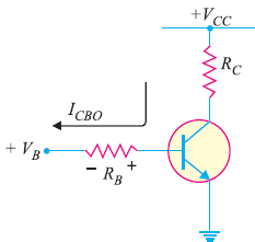
The reverse leakage current ICBO has the effect of decreasing the net base current and thus increasing the base voltage. It is because the flow of ICBO creates a voltage drop across RB that adds to the base voltage as shown in Fig. 6. Therefore, change in ICBO shifts the Q-point of the base bias circuit.
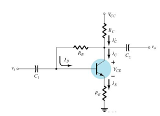
Fig.
However, in modern transistors, ICBO is usually less than 100 nA and its effect on the bias is negligible if VBB >> ICBO RB.
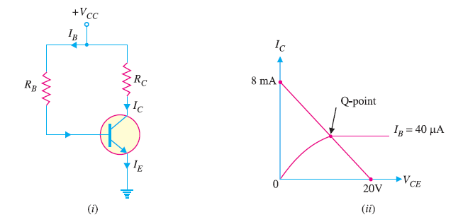
Q7) For figure below is a resistor transistor circuit. The device has the characteristics as shown below. Find VCC, RC and RB?

Solution:
The DC Line voltage VCC = 20V
Maximum IC = VCC/RC
RC = 20/8x10-3=2.5k
IB = VCC – VBE/RB
RB = 20-0.7/40x10-6 = 482.5k
Fixed Bias Configuration

Fig 28 Fixed Biasing Circuit JFET
Fixed dc bias is obtained using a battery VQG. This battery ensures that the gate is always negative with respect to source and no current flows through resistor RG and gate terminal that is IG =0. The battery provides a voltage VGS to bias the N-channel JFET, but no resulting current is drawn from the battery VGG. Resistor RG is included to allow any ac signal applied through capacitor C to develop across RG. While any ac signal will develop across RG, the dc voltage drop across RG is equal to IG RG i.e., 0 volt.
The gate-source voltage VGS is then
VGS = – VG – Vs = – VGG – 0 = – VGG
The drain -source current ID is then fixed by the gate-source voltage as determined by equation.
This current then causes a voltage drop across the drain resistor RD and is given as
VRD = ID RD and
output voltage
Vout = VDD – ID RD
Self-Bias Configuration
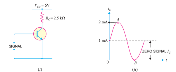
Fig 29 Self-Biasing for JFET
This is the most common method for biasing a JFET. Self-bias circuit for N-channel JFET is shown in figure.
Since no gate current flows through the reverse-biased gate-source, the gate current IG = 0 and, therefore,
vG = iG RG = 0
With a drain current ID the voltage at the S is
Vs= ID Rs
The gate-source voltage is then
VGs = VG – Vs = 0 – ID Rs = – ID Rs
So, voltage drop across resistance Rs provides the biasing voltage VGg and no external source is required for biasing and this is the reason that it is called self-biasing.
The operating point (that is zero signal ID and VDS) can easily be determined from equation and equation given below:
VDS = VDD – ID (RD + RS)
Thus, dc conditions of JFET amplifier are fully specified. Self-biasing of a JFET stabilizes its quiescent operating point against any change in its parameters like transconductance. Let the given JFET be replaced by another JFET having the double conductance then drain current will also try to be double but since any increase in voltage drop across Rs, therefore, gate-source voltage, VGS becomes more negative and thus increase in drain current is reduced.
Key takeaway
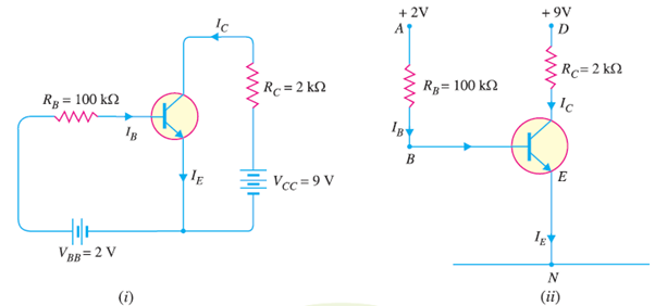
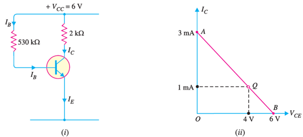
Fig 30 Voltage Divider Bias Circuit for JFET
The resistors RGl and RG2 form a potential divider across drain supply VDD. The voltage V2 across RG2 provides the necessary bias. The additional gate resistor RGl from gate to supply voltage facilitates in larger adjustment of the dc bias point and permits use of larger valued RS.
The coupling capacitors are assumed to be open circuit for DC analysis
1) The gate is reverse biased so that IG = 0 and gate voltage
VG =V2 = (VDD/RG1 + R G2) *RG2
2) Applying KVL to the input circuit we get
VGS= VG – VS = VG - ID RS
3) IDQ= IDSS (1- VGS/ VP)2
4) VDS = VDD – ID (RD + RS)
The operating point of a JFET amplifier using the Voltage -Divider Bias is determined by
IDQ= IDSS (1- VGS/ VP)2
VDSQ = VDD – ID (RD + RS)
VGSQ = VG – ID RS
Design
Q1) Determine IDQ, VGSQ, VD, VS, VDS, and VDG?
Sol:
VG = VDDR2/R1+R2 = (16x270K)/(2.1M+270K) = 1.823V
VGS = 1.823- ID RS = 1.823 – 1.5x10³ ID
ID = IDSS (1-VGS/VP)2 = 8x10⁻³ (2.12-1092ID+140625ID2)
1125 ID2-9.736ID+0.01696=0
ID= 2.417mA
Discard other value as its not feasible.
VDS= VDD -ID (RD + RS) = 16- 2.417x10⁻³(2.4K+1.5K) = 6.5737V
VGS = 1.823- ID RS = 1.823 – (1.5x103x2.417x10-3) = -1.8025V
V= = ID RS = 2.417x10-3 x 1.5x103 = 3.6255V
VD = VDD – ID RD = 16- 2.417x10⁻³(2.4K) = 10.2V
VDG = VD – VG = 10.2 – 1.823 =8.377V
Q2) Calculate the value of feedback resistor Rs required to self-bias JFET with IDSS= 40mA, VP= -10 and VGSQ= -5V?
Sol:
IDQ =IDSS [1-(VGSQ/VP)]2
= 40x10-3 [1- {(-5)/ (-10)}]2 = 10mA
For self-bias VGSQ = - IDQ RS
RS = -VGSQ/IDQ = -(-5)/10mA = 500Ohm
Q3) For the circuit shown below the FET has VP= 4V, IDSS = 4mA. Calculate IDSQ, VGSQ and VDSQ?
Sol:
The simplified circuit will be
VG = R2 VDD/ (R1 + R2) = (200x10-3x(-60))/(1.3x106+200x103) = -8V
VG – VGS +ID RS = 0
VGS = -8 + ID RS
Finding ID
ID = IDSS (1-VGS/VP)2 = 2.25mA or 4mA
As the given circuit is of p-channel FET so VDS should be negative. For ID =2.25mA the value of VDS is negative.
VDS= VDD -ID (RD + RS) = -60-(-2.25m (4000+18000)) = -10.5V
VGS = -8 +ID R= = 1V
References:
1. Microelectronics Circuits, Adel Sedra and Kenneth C Smith, Oxford University Press, New Delhi, 5th Edition, International Student Edition,2009. (Selected portion of Chapter 2,4, 5, 6, 8, 13, and 14)
2. Electronic Devices and Circuits theory, R.L. Boylestad and L. Nashelsky, Pearson Education, New Delhi, 9th/10th Edition,2013. (Selected portions of Chapter 4, 5, 6, 7, 8, 9, 10, 11, 12, and 14)
3. Milliman’s Electronics Devices and Circuits, J. Milliman, C. Halkias, S. Jit., Tata McGraw Hill