Unit - 3
High Frequency Response of FETs and BJTs
High Frequency equivalent models and frequency response of BJT

Fig 1 Transistor model

Fig 2 Hybrid equivalent pi-model
Ci = cwi + cbe + cbc(1-av) Co = cwo + cce + cbc(1-AV)
= cwi + cbe + cmi = cwo + cce + cmo
Where cmi = input miller capacitance where cmo = o/p miller capacitance
At increasing frequencies, the reactance xc will decrease in magnitude resulting in a shorting effect across the output and a decrease in gain.
For high frequency response, various parasite capacitances (cbe, cbc, cce) of the transistors are included along with the wiring capacitors (cwi, cwo) for analysis.
For high frequency response, cs, cc, ce are assumed to be in short circuit state.
Input capacitance ci includes wiring capacitance cwi, the transistor capacitance.
Cbe and miller capacitance cmi.
The o/p capacitance co includes wiring cce and miller capacitance cmo
Cmi = cbc (1-av)
Cmo = cbc (1−11−1/av)
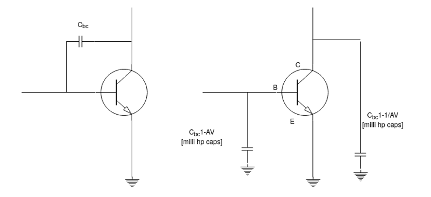
Fig 3 Output capacitance
For the input network, the – 3db frequency is defined by

rthi = rsrs // r1r1 // r2r2 // rππ
ci = cwi + cbc + cmi
cmi = cbc (1-av)
at very high frequency, the effect of ci is to reduce the total impedance of the parallel combination of r1r1, r2r2, rπrπ & ci. The route is a reduced level of voltage across ci, a reduction in In and a gain for the system.

Rtho = rc // rlrl // re
c0c0 = cwot + cce + cmo
Cme = cbe (1 - 1av)1av)
∵∵ 1 >> yav cmo = cbc
At very high frequency, XCO will decrease and consequently reduced the total impedance of o/p parallel branches. The net result is vo will also decline towards ‘o’ as the reactance xc becomes (zero) or smaller.
High Frequency equivalent models and frequency response of FET
The high frequency equivalent circuit for an FET is obtained by adding internal capacitors between each pair of transistor terminals as shown in the figure to the right. The FET capacitances shown on data sheets are given as the equivalent input capacitance (Ciss), the forward transfer capacitance (Cfs), the reverse transfer capacitance (Crss) and the output capacitance (Cos), where
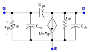
Fig 4. FET high frequency model
Ciss = Cgs + Cgd
Cfs = Cgd
Crss = Cgd
Cos = Cgd + Cds
The relation of capacitors can be given as
Cgd = Crss
Cgs = Ciss – Crss
Cds = Cos – Crss
rgs may be considered as an open circuit. The input resistance is usually around 1 to 10 MΩ for JFETs and even larger for MOSFETs, so it may be ignored. Cds is very small, so the impedance contribution of this capacitance may be considered to be an open circuit and may be ignored. Miller’s theorem may be used to replace the series capacitance, Cgd, with shunt capacitances in the input and output circuit as follows
CN1 = Cgd (1-AV)
CN2 = Cgd (1-1/AV)
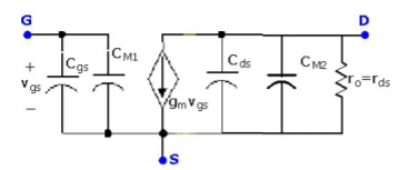
Fig 5 Reduced Equivalent Circuit
The simplified equivalent circuit for the high frequency response of an FET is shown to the right and is based on Figure. Often this circuit may be further simplified by ignoring the output resistance, rds, since it is usually larger than any resistance connected to the drain terminal. For the CB BJT amplifier, also hold for the common-gate amplifier configuration, where Cb’e is replaced with Cgs, re is replaced with 1/gm, Cb’c is replaced with Cgd, and appropriate changes are made to external component notation. The definition of time constants and pole frequencies in Section H5, for the CC (EF) BJT amplifier, also hold for the common-drain, or source follower, amplifier configuration, where Cb’e is replaced with Cgs, Cb’c is replaced with Cgd, and appropriate changes are made to external component notation.
Key takeaway
The high frequency equivalent circuit for an FET is obtained by adding internal capacitors between each pair of transistor terminals
The JFET implementation of the common-source amplifier is given to the left below, and the small signal circuit incorporating the high frequency FET model is given to the right. As stated above, the external coupling and bypass capacitors are large enough that we can model them as short circuits for high frequencies
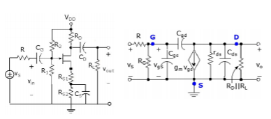
Fig 6 High frequency response of CS amplifier
We may simplify the small signal circuit by making the following approximations and observations: rds is usually larger than RD||RL, so that the parallel combination is dominated by RD||RL and rds may be neglected. If this is not the case, a single equivalent resistance, rds||RD||RL may be defined. The Miller effect transforms Cgd into separate capacitances seen in the input and output circuits as
CN1 = Cgd (1-AV)
CN2 = Cgd (1-1/AV)
The parallel capacitances in the input circuit, Cgs and CM1, may be combined to a single equivalent capacitance of value
Cin = Cgs + CN1 = Cgs + Cgd (1- AV)
Similarly, the parallel capacitances in the output circuit, Cds and CM2, may be combined to a single equivalent capacitance of value
Cout = Cds + CN2 = Cds + Cgs (1-1/AV)
where Av=-gm (RD||RL) for a common-source amplifier. The simplified circuit will be given as

Fig 7 Equivalent Circuit
Cin: Setting Cpit and CS equal resistance seen by Cin is RCin = R|| RG.
Cout: Letting the impedance of Cin be equal to infinity, the equivalent resistance seen by Cout is
Rcout = Ro || RL
The high frequency time constants for the CS amplifier are given as
Rcin = Cin Rcin
rcout = Cout Rcout
The upper corner frequency is given by

The general cut-off frequency is given by

Key takeaway
The parallel capacitances in the input circuit, Cgs and CM1, may be combined to a single equivalent capacitance of value
Cin = Cgs + CN1 = Cgs + Cgd (1- AV)
At high frequencies, internal transistor junction capacitances do come into play, reducing an amplifier's gain and introducing phase shift as the signal frequency increases.
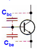
Fig 8 Internal transfer junction capacitances
At lower frequencies, the internal capacitances have a very high reactance because of their low capacitance value (usually only a few pf) and the low frequency value. Therefore, they look like opens and have no effect on the transistor's performance. As the frequency goes up, the internal capacitive reactance's go down, and at some point, they begin to have a significant effect on the transistor's gain.
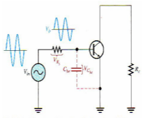
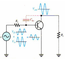
Fig 9 High Frequency Equivalent
When the reactance of Cbe becomes small enough, a significant amount of the signal voltage is lost due to a voltage-divider effect of the source resistance and the reactance of Cbe. When the reactance of Cbc becomes small enough, a significant amount of output signal voltage is fed back out of phase with the input (negative feedback), thus effectively reducing the voltage gain.
The Miller effect occurs only in inverting amplifiers –it is the inverting gain that magnifies the feedback capacitance.

Fig 10 Miller Equivalent
Miller's theorem is used to simplify the analysis of inverting amplifiers at high-frequencies where the internal transistor capacitances are important. Av is the voltage gain of the amplifier at midrange frequencies, and C represents Cbc
Miller theorems state that C effectively appears as a capacitance from input to ground and can be expressed as follows:
Cin(Miller) = C (A v +1)
Miller's theorems also state that C effectively appears as a capacitance from output to ground and can be expressed:
Cout (Miller) = C (Av +1)/Av
This indicates that if the voltage gain is 10 or greater Cout (Miller) is approximately equal to Cbc because (Av + 1) / Av is equal to 1
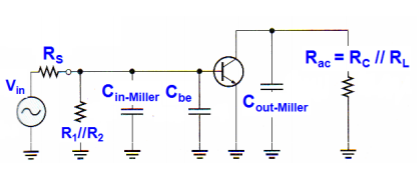
Fig 11 High Frequency Miller Model
As the frequency increases, the capacitive reactance becomes smaller. This causes the signal voltage at the base to decrease, so the amplifier's voltage gain decreases. The reason for this is that the capacitance and resistance act as a voltage divider and, as the frequency increases, more voltage is dropped across the resistance and less across the capacitance.
At the critical frequency, the gain is 3 dB less than its midrange value. Just as with the low frequency response, the critical high frequency, fc, is the frequency at which the capacitive reactance is equal to the total resistance
Xc = 1/2πfcCtotal
= Rs||R1||R2|| re’
re’
fc = 1/2π(Rs||R1||R2|| re’) Ctotal
Ctotal = Cbe + Cin −Miller
Total High frequency Response of CE Amplifier
The two RC circuits created by the internal transistor capacitances influence the high frequency response of BJT amplifiers. As the frequency increases and reaches the high end of its midrange values, one of the RC will cause the amplifier's gain to begin dropping off. The frequency at which this occurs is the dominant critical frequency; it is the lower of the two critical high frequencies. At fc(input) the voltage gain begins to roll off at -20dB/decade. At fc(output), the gain begins dropping at -40 dB/decade because each RC circuit is providing a -20 dB/decade roll -off.

Fig 12 Total high frequency response of CE Amplifier
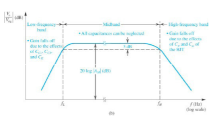
Fig 13 Total frequency response of CE amplifier
Key takeaway
As the frequency increases, the capacitive reactance becomes smaller. This causes the signal voltage at the base to decrease, so the amplifier's voltage gain decreases. The reason for this is that the capacitance and resistance act as a voltage divider and, as the frequency increases, more voltage is dropped across the resistance and less across the capacitance.
References:
1 “Electronic Devices and Circuit Theory”, Boylestad and Nashelsky, PEARSON
PUBLICATION.
2 “Electronic devices and circuits”, Salivahanan, Suresh Kumar, Vallavaraj,
TMH, 1999
3 “Integrated Electronics, Analog and Digital Circuits and Systems”, J. Millman
and Halkias, TMH, 2000
4 “Micro Electronic Circuits”, Sedra and Smith, Oxford University Press, 2000
5 “Electronic Devices and Circuits”, David A Bell, Oxford University Press, 2000