Unit - 4
Feedback amplifier and Oscillators
Positive Feedback amplifier– It is a type of an amplifier in which source signal and the feedback signal are in the same phase. Thus, the feedback signal applied increases the strength of the input signal.
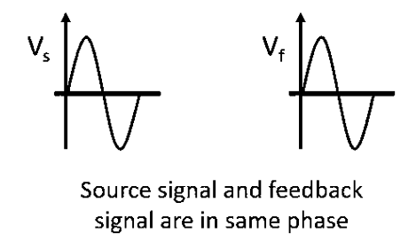
Fig 1 Signal in phase
Negative Feedback amplifier– In this type of amplifier source signal and the feedback signal are out of phase with each other. Thus, the feedback signal applied to decrease the strength of the input signal.

Fig 2 Signal out of phase
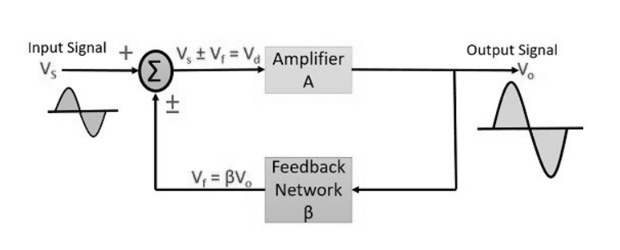
Fig 3 Feedback Amplifier
An input signal Vs is applied to the amplifier with gain A, that produces an amplified signal, Vo.
A portion or fraction of this Vo is then fed to a feedback network having gain β. The output of feedback network is Vf, this signal is then given to summer or a mixer that resultantly produces either sum or difference of two signal depending on their phase relationship.
The gain of an amplifier is given as the ratio of output voltage or current to the input voltage or current.
Key takeaway
Though the gain of negative feedback amplifier is reduced, there are many advantages of negative feedback such as
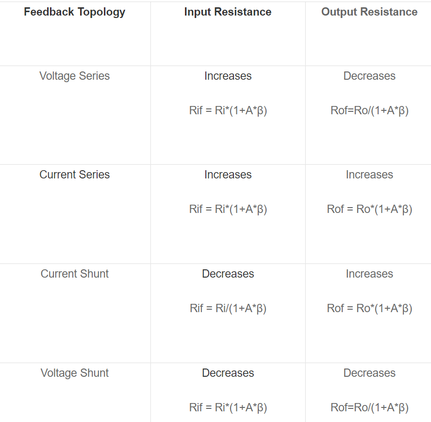
There are four basic feedback amplifiers on the basis of current and voltages as feedback.

Fig 4 Voltage Series Feedback amplifier
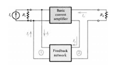
Fig 5 Voltage Shunt Feedback Amplifier
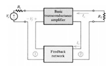
Fig 6 Current Series Feedback Amplifier
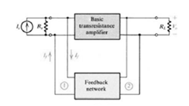
Fig 7 Current Shunt Feedback Amplifier
Key takeaway
An input signal Vs is applied to the amplifier with gain A, that produces an amplified signal, Vo.
A portion or fraction of this Vo is then fed to a feedback network having gain β. The output of feedback network is Vf, this signal is then given to summer or a mixer that resultantly produces either sum or difference of two signal depending on their phase relationship.
The gain of an amplifier is given as the ratio of output voltage or current to the input voltage or current.
The gain of the circuit without feedback is given as
A= Vo/Vd -----------------(1)
The gain of feedback network is given as
β = Vf/Vo ----------------(2)
Vd is the mixer output voltage given by
Vd = Vs ± Vf --------------------------(3)
The signal voltage Vs and mixer output voltage Vd will only be equal in a feedback amplifier unless the output is not generated.
From Eq 1 we can write as
Vo = A Vd -----------------------------------(4)
Substituting the value Vd in eq 4
Vo = A [ Vs ± Vf] -------------------------------(5)
From Eq 2
Vf = β Vo ------------------------------------(6)
Substituting the value of Vf in eq 5
Vo = A [ Vs ± β Vo]
Vo = A Vs ± A β Vo
Vo ± A β Vo = A Vs
Vo [1± Aβ] = A Vs
Vo/Vs = A / 1 ± Aβ
Avf = A/ 1 ± Aβ where Vo/Vs = Avf
This is the desired value for the gain of the feedback amplifier.
The gain of an amplifier is always greater than 1. This simply means that some elements are present which increases the gain of the amplifier. That element can be a transistor or a MOSFET.
But a feedback network is always a linear network consisting of RLC elements and it does not contain any such amplification device.
That’s why the value of Vf is always less than Vo.
So, β < 1
In case of a positive feedback the source signal will be in phase with that of the feedback signal.
Thus, the mixer will produce the summation of the two-signal applied to it in case of positive feedback.
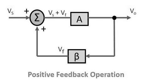
Fig 8 Positive Feedback Amplifier
So, the gain of the amplifier is given as
Avf = A/ 1 - Aβ
This is the gain for a positive feedback amplifier.
The source signal and the feedback signal are out of phase with respect to each other.
Thus, the mixer circuit will resultantly produce the difference between the two signals in case of a negative feedback amplifier.
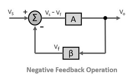
Fig 9 Negative Feedback
So, in this case, the gain of the amplifier is given as
Avf = A / 1+Aβ
For a negative feedback, the value of denominator is always greater than 1, this will decrease the overall gain of the system by the factor 1 +Aβ.
In case of a positive feedback system, the value of denominator is always less than 1, this will resultantly increase the overall gain by 1 – Aβ.
For an ideal system, the gain of the amplifier is infinite. Thus, for a smaller input, we will have a much higher value as output. So, such a large gain is not desirable in the circuit.
The system becomes stable only when its gain is small.
Hence, by decreasing the gain the stability of the system increases and vice-versa.
So, to have a stable system, the gain of the amplifier must be small and it is achieved by employing negative feedback in the circuit.
Key takeaway
These are known as harmonic oscillators and are LC tuned feedback or RC tuned feedback type oscillators that generate purely sinusoidal waveform which is constant in amplitude and frequency.
RC phase-shift oscillators use resistor-capacitor (RC) network as shown in Figure below to provide the phase-shift required by the feedback signal. They have excellent frequency stability and can yield a pure sine wave for a wide range of loads.
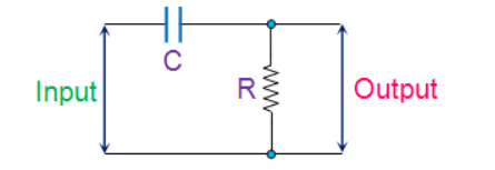
Fig 10 RC network
Ideally a simple RC network is expected to have an output which leads the input by 90o.The phase-difference will be less than this as the capacitor used in the circuit cannot be ideal.
Mathematically the phase angle of the RC network is expressed as
ɸ = tan -1 Xc / R
where, XC = 1/(2πfC) is the reactance of the capacitor C and R is the resistor. In oscillators, these kind of RC phase-shift networks, each offering a definite phase-shift can be cascaded to satisfy the phase-shift condition led by the Barkhausen Criterion.
LC Oscillators:
These are positive feedback oscillators. These oscillators produce regenerative feedback at the required frequency with the circuit components L, C and R forming a tank circuit. This feedback network is an attenuation network which has a gain of less than one (β <1) and starts oscillations when Aβ >1 which returns to unity (Aβ =1). The oscillator frequency is controlled by LC with the circuit output frequency.
The working of LC tank circuit is explained below. The simple way to understand the working is by understanding the working of components L and C. The capacitor stores the electrostatic energy in the form of potential, the inductor stores energy in its coil in the form of electromagnetic energy.

Fig 11: LC Tank Circuit
The capacitor is charged to voltage V, after it gets fully charged the switch changes its position. This charged capacitor then discharges itself through the inductor. The current through L increases and voltage across C decreases. As there is now no external voltage in the circuit to maintain the current within the coil, it starts to fall as the electromagnetic field begins to collapse.
A back emf is induced in the coil (e = -Ldi/dt) keeping the current flowing in the original direction. This current charge up capacitor, C with the opposite polarity to its original charge. C continues to charge up until the current reduces to zero and the electromagnetic field of the coil has collapsed completely. The above process is repeated and the LC oscillator works.
The frequency of oscillator voltage depends on L and C. The circuit is at resonance when XC =XL. The resonant frequency curve is shown below.

Fig 12: Resonant Curve
XL = 2 f L
f L
XC = 
At resonance XL = XC
2 f L =
f L = 
The resonant frequency is then given as
fr = 
LC oscillator using BJT
Here the LC circuit is connected across the load. The coil L2 is connected between base and emitter of transistor which is mutually coupled with coil L. Due to mutual induction the current flowing in one is induced in the other.
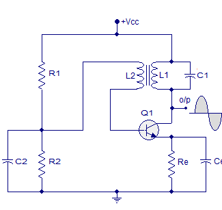
Fig 13 LC Oscillator using BJT
The electromagnetic energy is transferred from coil L to coil L2 and a voltage of the same frequency as that in the tuned circuit is applied between the base and emitter of the transistor. The circuit impedance at oscillation is resistive and the CB voltages are 180o out of phase. So, additional 180o phase shift is introduced through feedback path.
Key takeaway
These are known as harmonic oscillators and are LC tuned feedback or RC tuned feedback type oscillators that generate purely sinusoidal waveform which is constant in amplitude and frequency.
Wein Bridge Oscillators
Wien bridge oscillator is an audio frequency sine wave oscillator of high stability and simplicity. The feedback signal in this circuit is connected to the non-inverting input terminal so that the op-amp is working as a non-inverting amplifier.
The feedback network does not provide any phase shift. The circuit can be viewed as a Wien bridge with a series combination of R1 and C1 in one arm and parallel combination of R2 and C2 in the adjoining arm. Resistors R3 and R4 are connected in the remaining two arms.
The condition of zero phase shift around the circuit is achieved by balancing the bridge. The series and parallel combination of RC network form a lead-lag circuit.
At high frequencies, the reactance of capacitor C1 and C2 approaches zero. This causes C1 and C2 appears short. Here, capacitor C2 shorts the resistor R2. Hence, the output voltage Vo will be zero since output is taken across R2 and C2 combination. So, at high frequencies, circuit acts as a 'lag circuit'.
At low frequencies, both capacitors act as open because capacitor offers very high reactance. Again, output voltage will be zero because the input signal is dropped across the R1 and C1 combination. Here, the circuit acts like a 'lead circuit'.
But at one particular frequency between the two extremes, the output voltage reaches to the maximum value. At this frequency only, resistance value becomes equal to capacitive reactance and gives maximum output. Hence, this frequency is known as oscillating frequency (f).
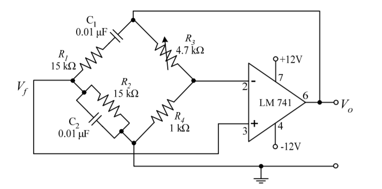

Consider the feedback circuit, on applying voltage divider rule
Vf(s) = Vo(s) x Zp(s)/ Zp(s) + Zs(s)
Zs(s) = R1 + 1/sC1 and Zp(s) = R2|| 1/sC2
Let R1=R2=R and C1=C2=C. On solving
β = Vf(s)/ Vo(s) = RsC /(RsC) 2 + 3RsC + 1 ---------------------------(1)
Since the op-amp is operated in the non-inverting configuration the voltage gain
Av = Vo(s)/ Vf(s) = 1 + R3/R4 -------------------(2)
Applying the condition for sustained oscillations, = Av β =1
RsC /(RsC) 2 + 3RsC + 1. 1 + R3/R4
S=jw
(1 + R3/R4) (jwRC/ - R2 C2 w2 + 3 jwRC + 1) =1
jw RC (1 + R3/R4) = (- R2 C2 w2 + 3 jwRC + 1)
jw [(1 + R3/R4) RC – 3RC] = 1- R2 C2 w2
To obtain the frequency of oscillation equate the real part to zero
1- R2 C2 w2 = 0
w = 1/RC
f = 1/ 2 π RC
To obtain the condition for gain at the frequency of oscillation equate the imaginary part to zero.
jw [(1 + R3/R4) RC – 3RC] = 0
jw [(1 + R3/R4) RC= jw3RC
[(1 + R3/R4) =3
R3/R4 =2
Therefore R3 = 2 R4 is the required condition.
Phase Shift oscillator

In an RC Oscillator circuit, the input is shifted 180o through the feedback circuit returning the signal out-of-phase and 180o again through an inverting amplifier stage to produces the required positive feedback.
This then gives us “180o + 180o = 360o” of phase shift which is effectively the same as 0o, thereby giving us the required positive feedback.
In other words, the total phase shift of the feedback loop should be “0” or any multiple of 360o to obtain the same effect.
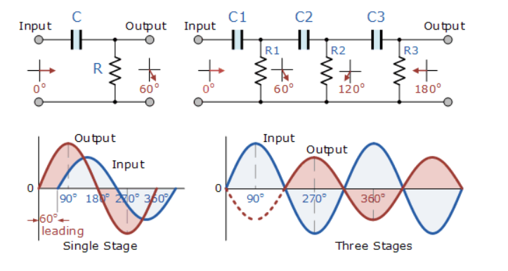
The circuit on the left shows a single resistor-capacitor network whose output voltage “leads” the input voltage by some angle less than 90o.
In a pure or ideal single-pole RC network. it would produce a maximum phase shift of exactly 90o, and because 180o of phase shift is required for oscillation, at least two single-poles networks must be used within an RC oscillator design.
However, in reality it is difficult to obtain exactly 90o of phase shift for each RC stage so we must therefore use more RC stages cascaded together to obtain the required value at the oscillation frequency.
The amount of actual phase shift in the circuit depends upon the values of the resistor (R) and the capacitor (C), at the chosen frequency of oscillations with the phase angle (φ) being given as:
Xc = 1/2π fc R=R
Z = [ R 2 + Xc 2] ½
Ø = tan -1 Xc /R
Crystal Oscillator
Crystal Oscillator can be designed by connecting the crystal into the circuit such that it offers low impedance when operated in series-resonant mode and high impedance when operated in anti-resonant or parallel resonant mode as shown below in figure a and b respectively.

Fig 14(a) Series Resonance Fig 14(b) Parallel Resonance
In the circuits shown, the resistor R1 and R2 form the voltage divider network while the emitter resistor RE stabilizes the circuit. Further, CE (Figure a) acts as an AC bypass capacitor while the coupling capacitor CC (Figure a) is used to block DC signal propagation between the collector and the base terminals. Next, the capacitors C1 and C2 form the capacitive voltage divider network in the case of Figure b.
In addition, there is also a Radio Frequency Coil (RFC) in the circuits (both in Figure a and b) which offers dual advantage as it provides even the DC bias as well as frees the circuit-output from being affected by the AC signal on the power lines.
On supplying the power to the oscillator, the amplitude of the oscillations in the circuit increases until a point is reached wherein the nonlinearities in the amplifier reduce the loop gain to unity. Next, on reaching the steady-state, the crystal in the feedback loop highly influences the frequency of the operating circuit.
Further, here, the frequency will self-adjust so as to facilitate the crystal to present a reactance to the circuit such that the Barkhausen phase requirement is fulfilled.
In general, the frequency of the crystal oscillators will be fixed to be the crystal’s fundamental or characteristic frequency which will be decided by the physical size and shape of the crystal.
However, if the crystal is non-parallel or of non-uniform thickness, then it might resonate at multiple frequencies, resulting in harmonics. Further, the crystal oscillators can be tuned to either even or odd harmonic of the fundamental frequency, which are called Harmonic and Overtone Oscillators, respectively.
Key takeaway
Crystal Oscillator can be designed by connecting the crystal into the circuit such that it offers low impedance when operated in series-resonant mode and high impedance when operated in anti-resonant or parallel resonant mode.
The position of the Q-point and the extent of the characteristics that is being used, decides the class of operation of power amplifiers.
The various classes of power amplifiers are –
(i) Class A power amplifier
(ii) Class B power amplifier
(iii) Class C power amplifier
(iv) Class AB power amplifier
1). The intersection of the output characteristics curve and the load line is known as operating point or Q-point of transistor.
2). On this quiescent operating point, if an a.c. signal is superimposed by the application of a.c. sinusoidal voltage at the input, the base current varies sinusoidally about its quiescent value IBQ.
3). Since the transistor is biased to operate in the active region, the output is linearly proportional to the input i.e., IC = βIB
4). Hence the collector current also varies sinusoidally about its quiescent value IBQ.
Class A amplifier: A class-A amplifier is the amplifier in which the Q-point of the input signal are selected such that the output signal is obtained for a full input cycle. For this purpose, the position of the Q-point is approximately at the midpoint of the load line.
For all the values of the input signal, the transistor remains in the active region and never enters into cut-off or saturation region.
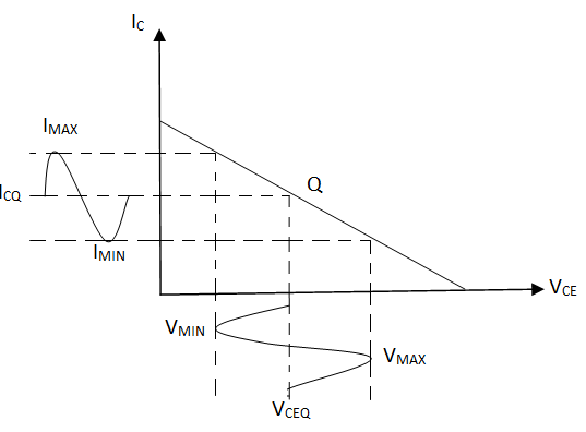
Fig 15 Output characteristics of CE Amplifier
The collector current IC flow for complete 3600 (full cycle) of the input cycles. Thus, the angle of the collector current flow is 3600.
Class A amplifier are of 2 types –
(i) Directly coupled class A amplifier – In directly coupled type, the load is directly connected in the collector circuit.
(ii) Transformer coupled class A amplifier – In this the load is coupled to the collector using a transformer called an output transformer.
(i) Directly coupled class A amplifier –

Fig 16 Directly coupled class A amplifier
The value of RB is selected such that Q point lies at the centre of d.c. load line.
VCC = ICRL + VCE
IBQ = VCC – 0.7 / RB
ICQ = βIBQ
VCEQ = VCC - ICQRL
DC power input: PDC = VCCICQ Watts
The d.c. power input is provided by the supply:
A.C. power Output:
Vpp = Vmax - Vmin
Vmin = Min instantaneous value of collector output voltage
Vmax = Max instantaneous value of collector output voltage
Vpp = Peak of a.c. output voltage
Vm = Vpp / 2 = Vmax – Vmin / 2 = Amplitude of a.c. output voltage
Im = Ipp / 2 = Imax – Imin / 2
The r.m.s value of alternating output voltage and current is given as
Vrms = Vm / √2 ;Irms = Im / √2
Pac = VrmsIrms = I2rmsRL = V2rms / RL
Pac = Vm /√ 2: Im /√ 2 = 1/2Vmax – Vmin /√ 2. Imax – Imin /√ 2
Pac = ( Vmax - Vmin )( Imax - Imin ) / 8
Efficiency:
% n = Pac / Pdc x 100 %
= [(Vmax - Vmin) (Imax - Imin) / 8 x Vcc x ICQ] x 100%
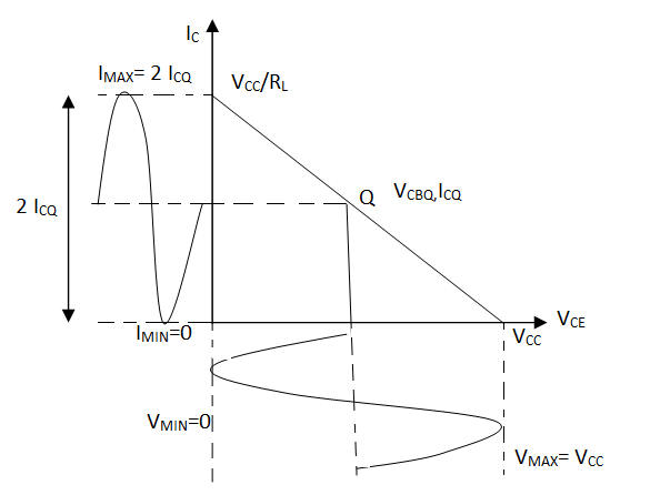
Fig 17 AC Power Output
Maximum Efficiency:
Vmax = Vcc, Vmin = 0
Imax = 2ICQ, Imin = 0 {As Q is in middle}
n = (Vmax - Vmin) (Imax - Imin) / 8 x Vcc. ICQ x 100 %
= (Vcc - 0) (2ICQ - 0) / 8 x Vcc.ICQ x 100 %
Nmax = 25 % {Biggest disadvantage}
Power dissipation ( Pd ): Pd = Pdc - Pac
Power dissipation = D.C. power input – AC power output
(i) When there is no input signal, then Pac = 0 and the entire d.c power gets dissipated in the form of heat which is maximum PD.
(Pd)max = PDC = VCCICQ when Pac = 0
(ii) When input signal is larger, more power is delivered to load (Pac is more) and less is the power dissipation.
Thus, class A amplifier dissipated less power when delivers maximum power to the load while it dissipates maximum power while delivering zero power to the load.
Disadvantages:
(i) The load resistance is connected directly to collector, hence quiescent current passes through this resistance. This current represents a considerable waste of power, since it doesn’t contribute to the a.c. component of the power. Also, it is inadvisable to pass the d.c. component of current through the output device.
(ii) Efficiency is poor.
(ii) Transformer coupled Amplifier:
Generally, the output impedance of the transistor is much higher than the input impedance (RL) of the loudspeaker. Hence most of the power generated would be lost in the transistor.
To transfer a significant amount of power to the load, it is necessary to use an output matching transistor.
Applying KVL: VCC – VCEQ = 0 => VCEQ = VCC
DC power input: PDC = VCCICQ
Where,
RL = load on secondary
R2 = Reflected load on the primary or effective load as seen by primary
RL1 = (N1 / N2 )2 RL
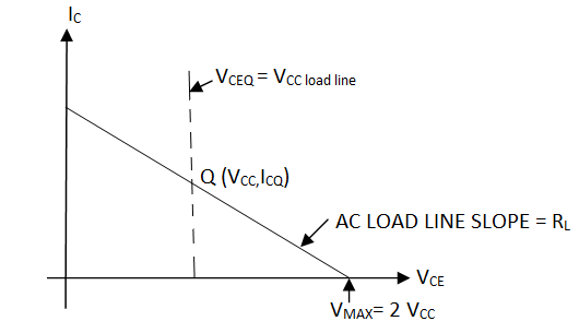
Fig 18 Load Line
AC power output Pac:
Pac = (Vmax - Vmin) (Imax - Imin) / 8
Pac = I12rmsRL1 = I22rmsRL = V1rmsI1rms = V2rmsI2rms
Where V1rms = RMS value of primary voltage
V2rms = RMS value of secondary voltage
Efficiency (n): n = Pac / Pdc x 100 %
Max efficiency:
Vmin = 0, Vmax = 2VCC
Imin = 0, Imax = 2ICQ
% nmax = 50 %
Class B amplifier– In class B amplifiers, the Q point and the input signal is selected, such that the output signal is obtained only for one half cycle for a full input cycle.
Either the quiescent current or the quiescent voltage is approximately zero. If quiescent current is zero, then the transistor is in cut off region, and the transistor remains in active region only for the half cycle of the input signal. Hence at output we get only the half cycle.
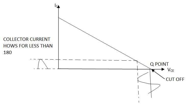
Fig 19 Load line characteristics of class B amplifier
If instead of ICQ = 0, we would have taken VCEQ = 0(i.e., Q point on Y-axis) then the transistor would have been in saturation region and the collector current flows only for negative half cycle of the input signal.
Efficiency of this mode is higher than class A mode.
Since in this mode, collector current flows only for half cycle, so that output signal is distorted. To get the full cycle, a pair of transistors is used in class B operation. The 2 transistors conduct in alternate half cycles of the input signal abd so a full cycle across the load is obtained. The two transistors are identical in characteristics and are called matched transistors.
Depending upon the types of 2 transistors, the two different circuit configurations of Class B are –
(i) Push Pull Class B amplifier
(ii) Complimentary Symmetry Class B
(i) Push Pull Class B amplifier: When both the transistors are of some type i.e., either n-p-n or p-n-p, then the circuit is called push-pull class B audio frequency power amplifier.
The push pull circuit requires 2 transformers, one as input transformer called driver transformer and the other to connect the load called output transformer. The input signal is applied to the primary of the driver transformer. Both the transformer is centre tapped transformers.
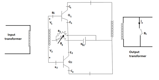
Fig 20 Push pull amplifier
In the circuit, both Q1 and Q2 are of n-p-n type. p-n-p can also be used but with -VCC. Both are in CE configuration.
Operation:
Case (i) – During positive half cycle,
Q1 = ON, Q2 = OFF
IO1α iC1
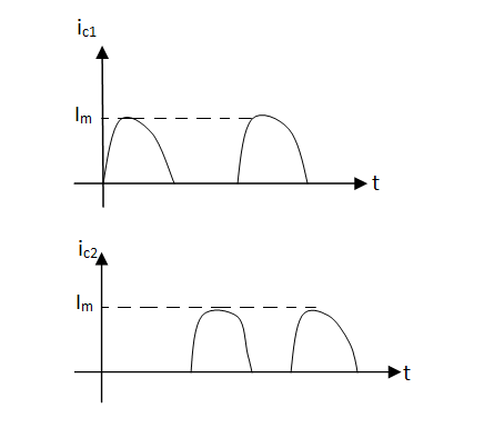
Fig 21 Positive half cycle output
Case (ii) – During negative half cycle,
Q1 = OFF, Q2 = ON
IO2α iC2
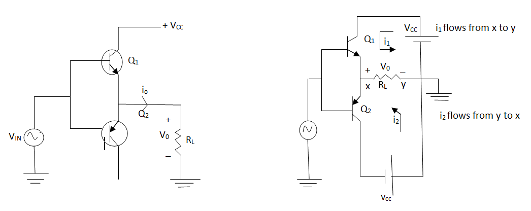
Fig 22 Positive half cycle output
Case (iii) When signal is absent i.e., V1 = V2 = 0
If R2 = 0 then,
VBE1 = VBE2 = 0
Both Q1, Q2 are in cut off [ Class B operation]
Case (iv) If R2 increases then IR2 increases and when IR2 = Vr then
VBE1 = VBE2 = Vr [ Class AB operation]
Case (v) If R2 increases more, then IR2 increases VBE increases and Q point will move towards saturation.
The total d.c. power is given by,
Pdc = VCC x Idc
= 2 / ∏ VCC Im
a.c. power, Pac = Vrms.Irms
= I2rmsR1L = V2rms / R1L
Efficiency:
% n = Pac / Pdc x 100 %
= ( Vm.Im / 2 ) / 2 / ∏VCCIm
% n = ∏ / 4 Vm / VCC x 100 %
Max Efficiency:
Max efficiency is possible only if, Vm = VCC
% nmax = ∏ / 4 VCC / Vcc x 100 = 78.5 %
Power dissipation:
Pd = Pdc - Pac
= 2 / ∏ VCCIm - Vm.Im / 2
= 2 / ∏ VCCVm/ R1L - Vm2 / 2 R1L
Maximum power dissipation:
For max power dissipation,
dPd / dVm = 2 / ∏ VCC / R1L - 2Vm/ 2 R1L = 0
2 / ∏ VCC / R1L = Vm/ R1L
Vm = 2 / ∏ VCC
This is the condition for max power dissipation,
Hence max power dissipation is given by,
(Pd)max= 2 / ∏ VCC x 2 / ∏ VCC / R1L - 4 / ∏2 VCC2 / 2R1L
= 4 / ∏2 VCC2 / R1L - 2 / ∏2 VCC2 / R1L
(Pd)max= 2 / ∏2 VCC2 / R1L
For max efficiency Vm = VCC hence the dissipation is not maximum when the efficiency is maximum and when power dissipation is maximum, efficiency is not maximum.
The a.c. power is given by,
Pac = Vm2 / 2RL1
Where Vm = VCC is the maximum condition.
The maximum a.c. power is given by
(Pac)max = VCC2 / 2RL1
(Pd)max = 2VCC2 / ∏2RL1 = 4 / ∏2( VCC2 / 2RL1 )
(Pd)max = 4 / ∏2 (Pac)max
The maximum power dissipation per transistor is given by,
(Pd)max per transistor = 4 / ∏2 (Pac)max / 2
= 2 / ∏2 (Pac)max
Advantages:
Disadvantages:
Complementary Symmetry Class B push pull amplifier –
This circuit is transformer less circuit. But with common emitter configuration, it becomes difficult to match the output impedance for maximum power transfer with output transformer. Hence the matched pair of complementary transistors is used in common collector (emitter follower) configuration in this circuit.
This is because common collector configuration has lowest output impedance and hence the impedance matching is possible.
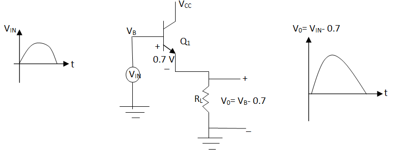
Fig 23 Complimentary symmetry Push pull amplifier
The circuit is driven from a dual supply of +-VCC. The transistor Q1 is n-p-n while Q2 is p-n-p type.
Operation:
During positive half cycle:

Fig 24 Positive half cycle operation
During negative half cycle:

Fig 25 Negative half cycle operation
Cross over distortion:

Fig 26 Crossover Distortion
Advantages:
(i) As the circuit is transformer less, its weight, size and cost are less.
(ii) Due to common collector configuration, impedance matching is possible.
(iii) The frequency response improves due to transformer less class B amplifier circuit.
Disadvantages:
(i) The circuit needs two separate voltage supplies.
(ii) The output is distorted to cross-over distortion.
Class AB amplifiers (between A and B):
In class AB amplifiers, the Q-point and the input signal are selected such that the output signal is obtained for more than a half cycle but less than a full cycle.

Fig 27 Characteristic curve for class AB operation
The Q point is below the midpoint but above X-axis or above the midpoint but to the right of Y-axis. Its efficiency is more than class A but less than class B. Efficiency increases as the Q-point moves away from the centre of the load line.
Key takeaway
Numerical:
Sol. Given: VL(p) = 20 V, RL = 16 Ω, VCC = 30 V
The input power is given by,
Pi(dc) = VCC(2 / ∏ I / p) = VCC.2 / ∏.VL(p) / RL
= 30 x 2 / ∏ x 20 / 16 = 23.87 W Ans.
The output power is given by,
PO(ac) = VL2(p) / 2RL = VL2(rms) / 2RL = (20)2 / 2 x 16 = 12.5 W Ans.
Thus, efficiency is given by,
n = PO(ac) / Pi(dc) x 100 = 12.5 / 23.87 x 100 = 52.37 % Ans.
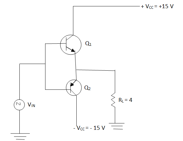
Q-2 – Class B complementary A.F. power amplifier shown in the below figure

Calculate:
Soln. Given: VC = 15 V, RL = 4 Ω
Use the expression derived for push pull class B.
(Pac)max = 1/2VCC2 / RL = 1/2(15)2 / 4 = 28.125 W Ans
RL = Vm / Im
Im= Vm / RL = VCC / RL = 15 / 4 = 3.75 A
Pdc = 2 / ∏VCCIm = 2 / ∏ x 1.5 x 3.75 = 35.809 W
Pd = Pdc – Pac = 35.809 – 28.125 = 7.684 W Ans.
This is the total collector dissipation under maximum power conditions.
% n = Pac / Pdc x 100 = 28.125 / 38.809 x 100 = 78.5 % Ans.
The efficiency is maximum possible for class B, due to the fact that the power developed is at its maximum.
Vm = 2 / ∏ VCC = 2 / ∏ x 15 = 9.5492 V
Im = Vm / RL = 9.5492 / 4 = 2.3873 A
Pdc = 2 / ∏ VCC Im = 2 / ∏ x 15 x 2.3873 = 22.797 W
While Pac = 1/2Vm2 / RL = 1/2(9.5492)2 / 4 = 11.398 W
(Pd)max = Pdc – Pac = 22.797 – 11.398 = 11.39 W
(Pd)max = 11.39 / 2 = 5.699 W [ Per transistor]
Alternatively, we can directly use the result,
(Pd)max = 2 / ∏2 (Pac)max per transistor
= 2 / ∏2 x 28.125 = 5.699 W per transistor Ans.
% n = Pac under (Pd)max / Pdc under (Pd)max x 100
= 11.398 / 22.797 x 100 = 50 % Ans.
This shows that when efficiency is maximum, power dissipation is not maximum and when power dissipation is maximum, efficiency is not maximum.
Q-3 – (A) A series fed class A amplifier uses a supply voltage of 10 V and load resistance of 20 Ω. The a.c. input voltage results in a base current of 4 mA peak. Calculate,
Assume β of the transistor as 25 and the collector bias current of 50 mA.
(B) Calculate the input power, output power & the efficiency of class A amplifier shown in figure. The input voltage causes a base current 5mA rms.

Sol :(A) Given: VCC = 10 V, (ib)m = 4 mA, β = 25, ICQ = 50 mA, RL = 20 Ω
PDC = VCCICQ = 10 x 50 x 10-3 = 0.5 W Ans.
(ic)m = β(ib)m = 25 x 4 = 100 mA
But ic is the output current I.
Im = 100 mA
Pac = I2mRL / 2 = (100 x 10-3)2 x 20 / 2 = 0.1 W Ans.
% n = Pac / Pdc x 100 = 0.1 / 0.5 x 100 = 20 % Ans
(B) Given class A amplifier is shown in below figure
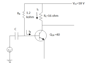
Current IBQ can be written as,
IBQ = VCC – 0.7 / RB = 18 – 0.7 / 1.2 x 103 = 14.4167 mA
Now, ICQ = βIBQ = 40 x 14.4167 = 576.67 mA
And, VCEQ = VCC – ICQ RL = 18 – 576.67 x 10-7 x 16 = 8.7733 V
So, Pdc = VCCICQ = 18 x 576.67 = 10.38 W Ans.
This is the input power.
(Ib)rms = 5 mA
(Ic)rms = β(Ib)rms = 40 x 5 = 200 mA
This is nothing but the output collector current r.m.s value Irms.
Irms = 200 mA
Output power can be written as,
Pac = I2rms RL = (200 x 10-3) x 16 = 640 mW
This is the power delivered to the load.
Hence the efficiency of the amplifier is,
% n = Pac / Pdc x 100 = 640 x 10-3 / 10.38 x 100
% n = 6.165 % Ans.
Q-4 - For a class B amplifier using common collector configuration, the supply voltage is 25 V while the load resistance is 16 Ω. If the input a.c. signal of 20 V peak is supplied, determine the input power, output power and the efficiency.
Sol. Given: VCC = 25 V, Vm = 20 V, RL = 16 Ω
For a common collector configuration, the voltage is 1.
Vin(peak) = Vout(peak) = 20 V
Now, Vm / Im = RL
Im = Vm / RL = 20 / 16 = 1.25 A
The input power is given by,
PDC = 2 / ∏ = VCCIm = 2 / ∏ x 25 x 1.25 = 19.8943 W Ans.
The output power is given by,
Pac = Vm Im / 2 = 20 x 1.25 / 2 = 12.5 W Ans.
Thus, efficiency is given by,
% n = Pac / Pdc x 100 = 12.5 / 19.8943 x 100 = 62.832 % Ans.
References:
1. Microelectronics Circuits, Adel Sedra and Kenneth C Smith, Oxford University Press, New Delhi, 5th Edition, International Student Edition,2009. (Selected portion of Chapter 2,4, 5, 6, 8, 13, and 14)
2. Electronic Devices and Circuits theory, R.L. Boylestad and L. Nashelsky, Pearson Education, New Delhi, 9th/10th Edition,2013. (Selected portions of Chapter 4, 5, 6, 7, 8, 9, 10, 11, 12, and 14)
3. Milliman’s Electronics Devices and Circuits, J. Milliman, C. Halkias, S. Jit., Tata McGraw Hill