Unit - 5
Operational Amplifier
Ideal Op-Amp
An op amp should also have very high open loop gain. In ideal cases, the input resistance and open loop gain of an op amp should be infinity whereas the output resistance would be zero. So, an ideal op amp should have following characteristics.
Characteristics | Value |
Open loop gain (A) | ∞ |
Input Resistance | ∞ |
Output Resistance | 0 |
Bandwidth Operation | ∞ |
Offset Voltage | 0 |
An ideal op amp is defined as, a differential amplifier with infinite open loop gain, infinite input resistance and zero output resistance. The ideal op amp has zero input current. This is because of infinite input resistance. As the input resistance of ideal op amp is infinite, an open circuit exists at input, hence current at both input terminals is zero.
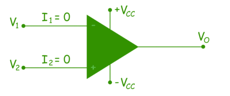
Figure. Ideal Op-amp
There is no current through the input resistance, there will be no voltage drop between the input terminals. Hence no offset voltage appears across the inputs of an ideal operational amplifier.
If v1 and v2 are the voltages of inverting and non-inverting terminals of op amp, and v1 = v2 then in ideal case,


The bandwidth of operation of an ideal op-amp is also infinite. That means the op-amp perform its function for all ranges of frequencies of operation.
Differential Amplifier is a device which is used to amplify the difference between the voltages applied at its inputs. Such circuits can be of two types viz.,

Figure. BJT Differential Amplifier
Here the input signals (V1 and V2) are applied to the base of the transistors while the output is collected across their collector terminals (Vo1 and Vo2).
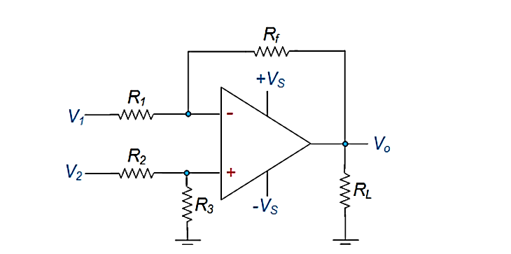
Figure. Differential Amplifier using Op-amp
Here V1 and V2 represent the voltages applied at its inverting and non-inverting input terminals and Ad refers to its differential gain.
The output of the differential amplifier is given as
Vo = Ad (V1 – V2) + Ac (V1 + V2/2)
where AC is called the common mode gain of the amplifier.
Hence its output voltage will be equal to the sum of the output voltages produced by the Op-Amp circuit operating as an inverting amplifier and the Op-Amp circuit operating as a non-inverting amplifier.
Thus, one gets,
Vo = -Rf/R1 V1 + V2. Rf / R2 + R3 (1 + Rf/R1)
Now, if R1 = R2 and R3 = Rf, then
Vo = -Rf/R1 V1 + V2. Rf/ R1 + Rf (R1 + Rf/R1)
Vo = - Rf/R1. V1 + V2. Rf /R1
Vo = - Rf/R1 (V1 – V2)
This implies that the gain of the differential amplifier circuit is given by -Rf/R1.
Key takeaway
The circuit is designed to have a VCE of 5V across Q2 and Q4. With a ±10 V supply and the bases of Q1 and Q2 at ground level, the voltage drops across R1 and R4 is 5.7 V and 4.3 V respectively. If the input voltage at Q1 base goes down to -4 V, the output terminal and Q2 base also goes down to -4 V as the output follows the input.
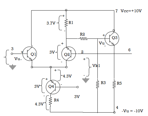
Fig. Input Voltage
This means that the emitter terminals of Q1 and Q2 are pushed down from -0.7 to -4.7 V. Consequently, the collector of Q4 is pushed down by 4 V, reducing VCE4 from 5 V to 1 V. Although Q4 might still be operational with a VCE of 1 V, it is close to saturation. It is seen that there is a limit to the negative going input voltage that can be applied to the op-amp if the circuit is to continue to function correctly.
There is also a limit to positive going input voltages. Where VB1 goes to +4 V, the voltage drop across resistor R1 must be reduced to something less than 1 V, in order to move VB2 and VE3 up by 4 V to follow the input. This requires a reduction in Ic2 to a level that makes Q2 approach cut-off. The input voltage cannot be allowed to become large enough to drive Q2 into cut-off
Output Voltage
The maximum voltage swing is limited by the input voltage range. The output voltage can swing in a positive or negative direction depends on the supply voltage and the op-amp output circuitry. The output voltage should be able to rise until Q5 is near saturation and fall until Q6 approaches saturation.
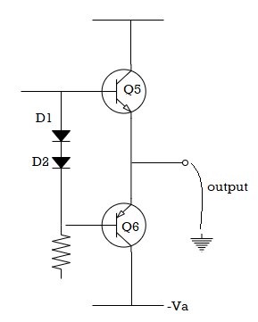
Fig. output voltage
But because of the circuits that control the output stage, is normally not possible to drive the output transistors close to saturation levels. A rough approximation for most op-amps is that the maximum output voltage swing is approximately equal to 1 V less than the supply voltage. For the 741 op-amp with a supply of ±15 V, the data sheet lists the output voltage swing as typically ±14 V.
Offset voltages
With an input offset voltage and a differential input circuit, ideal op-amps and comparators will have an offset voltage of 0V, including error voltage.
When inputting a common-mode (same) voltage to the input pins of an op-amp or comparator, with an ideal op-amp no output voltage will be output
In case where an input offset voltage exists, a voltage will be output based on the input offset voltage. This input offset voltage, which is the differential voltage required to make the output voltage 0V, becomes the input conversion value.
The Offset voltage is normally expressed in units of mV or µV. Values closer to 0 are more ideal.
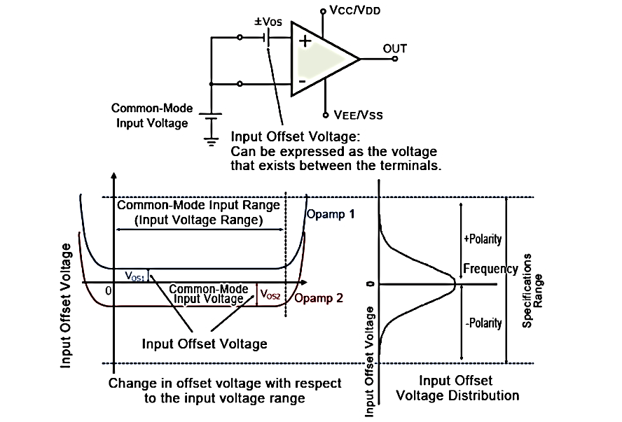
Fig. Op-Amp Parameters
The output offset voltage is the voltage at the output when the differential input voltage is zero.
Offset currents
difference between IB+ and IB-. This difference is called the offset current
|Ios| = IB+-IB------------------------- (7)
Offset current Ios for BJT op-amp is 200nA and for FET op-amp is 10pA. Even with bias current compensation, offset current will produce an output voltage when Vi = 0.
V1 = IB + R comp
And I1 = V1 R1
KCL at node a gives
I2 = (  – I1) =
  - (Ib + Rcomp/R1)
Again V0 = I2 Rf – V1
Vo = I2 Rf - IB+ Rcomp
Vo = 1M Ω X 200nA
Vo = 200mV with Vi = 0
Input and Output Impedance
The input impedance of op-amp is given as
Zif = (1+A )Zi
)Zi
Where:
A = Gain of op-amp
 = Feedback factor
Zi = Input impedance without feedback
The output impedance is given as
Zout = Z0/(1+A )
)
Zo = output impedance of op-amp
CMRR
It is the ratio of differential voltage gain Ad to the common mode voltage gain Acm.
CMRR = 
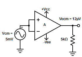
Fig. Common Mode Configuration
The common mode voltage gain from above figure can be
 =
= 
Where:
Vocm = output common mode voltage
Vcm = input common mode voltage
Acm = common mode voltage gain
In normal cases the value of Ad is large and Acm is very small making the value of CMRR very high.
Key takeaway
The common mode voltage gain from above figure can be
 =
= 
PSRR
PSRR = 
 = Change in input offset voltage
 = Change in supply voltage
Slew rate
For example, 1V/us indicates that the voltage can change by 1V in 1us. Ideal op-amps make it possible to faithfully output an output signal for any input signal. However, in reality slew rate limits do exist.
When supplying a rectangular pulse at the input with a steep rise and fall, this indicates the possible degree of change in the output voltage per unit time.

Fig. Voltage Follower
The rise and fall slew rates are calculated by the following equations:
SRr = ∆ V / ∆ Tr
SRf = ∆ V / ∆ Tf
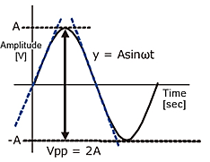
Fig. Slew Rate Calculation
Calculate the slew rate
The output is given by
y=Asinωt
The slew rate is the slope of the tangent of the sine wave, differentiating the above equation.
dy / = Aω cosωt ωt=0
Dt
The slew rate is
SR=Aω ω=2πf
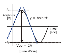
Fig. Sine wave amplitude
Since the amplitude of the sine wave becomes Vpp=2A (peak-to-peak), the equation can be modified as follows.

This frequency(f) is referred to as the full power bandwidth. These are conditions where the amplification factor in the op-amp has not been set, in other words the relationship of the frequency and amplitude (within the output voltage range) that can be output by the op-amp in a voltage follower circuit.
Key takeaways
Slew rate is the maximum rate of output voltage change per unit time. It is denoted by S. For getting undistorted output voltage we must have very high slew rate. It is measured in V/sec.
Frequency limitations
Fig below shows the graph of open loop gain (A) plotted versus frequency (f) for a 741 op-amp. f = 100 Hz, A = 80 dB f = 1 KHz, A = 60 dB

Fig. Frequency Response
The open loop gain (A) falls by 20 dB when the frequency increases from 100 Hz to 1 KHz. The ten times increase in frequency is termed a decade. So, the rate of the gain is said to be 20 dB per decade. Where internal gain equals to or greater than 80 dB is required for a particular application, it is available with a 741 only for signal frequencies up to ≈100 Hz. A greater than 20 dB is possible for signal frequencies up to ≈ 90 kHz. Other op-amp maintains substantial 1.3 OP-AMP AS DC AMPLIFIERS: Biasing op-amps internal gain to much higher frequencies than the 741
Non-inverting amplifier
Non- Inverting amplifier is one in which the output is in phase with respect to input that is if you apply a positive voltage, output will be positive. The output is a non -inverted amplified version of input.
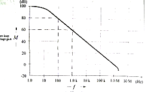
Fig. Non-inverting amplifier
Assuming the op-amp is ideal and applying the concept of virtual short, the voltage at the inverting terminal is equal to non- inverting terminal.
Applying KCL at inverting node we get
Vi -Vo/ R2 + Vo – 0 / R1 = 0
By rearranging the terms, we will get
Voltage gain Av = Vo/ Vi = (1+ Rf/Ri)
Gain of non- inverting amplifier Av= (1+ Rf/Ri).
Problem
Design a non-inverting amplifier using Op-amp with a closed loop voltage gain of 10.
Af = 1 + Rf/R1 =10
Rf/R1 = 9
Rf = 9 R1
If R1 = 1K
Rf = 9K Ω
Open-loop
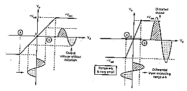
The voltage transfer curve indicates the inability of op-amp to work as a linear small signal amplifier in the open loop mode Such an open loop behaviour of the op-amp finds some rare applications like voltage comparator, zero crossing detector etc.
The configuration in which output depends on input, but output has no effect on the input is called open loop configuration.
• No feed-back from output to input is used in such configuration.
•The op-amp works as high gain amplifier
•The op-amp can be used in three modes in open loop configuration they are
• Differential amplifier Inverting amplifier
• Non inverting amplifier
Why op-amp is generally not used in open loop mode?
As open loop gain of op-amp is very large, very small input voltage drives the op-amp voltage to the saturation level. Thus, in open loop configuration, the output is at its positive saturation voltage (+Vsat) or negative saturation voltage (-Vsat) depending on which input V1 or V2 is more than the other. For a.c. input voltages, output may switch between positive and negative saturation voltages
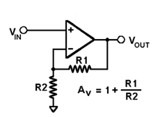
Fig. Open Loop Configuration
Closed-loop Gains
The utility of the op-amp can be increased considerably by operating in closed loop mode. The closed loop operation is possible with the help of feedback. The feedback allows to feed some part of the output back to the input terminals. In the linear applications, the op-amp is always used with negative feedback. The negative feedback helps in controlling gain, which otherwise drives the op-amp out of its linear range, even for a small noise voltage at the input terminals.
Key takeaway
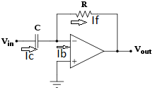
Differentiator
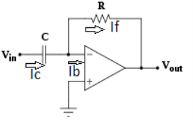
Fig: Differentiator

Since Ib = 0 then,
Ic ≈ If

Since Gain A is very large hence, V1 = 0

Or 
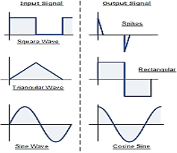
Fig: Input and output waveform of differentiator
 (For 0 db gain)
Practical differentiator with frequency response.
The noise and stability at high. frequency can be corrected, in the practical differentiator circuit using the resistance R1 in series with Cl and the capacitor C f in parallel with resistance R f.
The circuit is shown in the Fig. The resistance R comp is used for bias compensation.
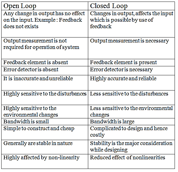
Fig: Practical Differentiator
As the input current of op-amp is zero, there is no current input at node B. Hence it is at the ground potential. From the concept of the virtual ground, node A is also at the ground potential and hence VB = VA = 0 V.
For the current I, we can write

where Z1 = Ri in series with C1
So, in Laplace domain we can write,
 R1 + 1/sC1


Now current I1 is,

In Laplace,


Taking Laplace we get,
I2 = -sCf Vo(s)
Applying node analysis at node A
I = I1 + I2
The time constant R 1C1 is much greater than R1C1 or R fC f and hence the equation (20) reduces to,
Thus, the output voltage is the RfCi times the differentiation of the input.
It may be noted that though R fel is much larger than RfCf or R1C1, it is less than or equal to the time period T of the input, for the true differentiation.

Applications
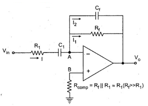
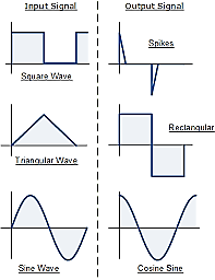
Fig: frequency response
Integrator
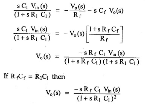
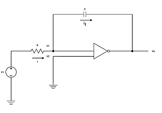
Fig 18 Integrator
Since the non-inverting input terminal of op-amp is grounded v2=0. Due to virtual short at the input of op-amp the inverting and non-inverting input terminals are at the same potential
Therefore v1=v2=0
Due to high impedance of op-amp the current flowing into its input terminal is zero. Therefore, the same current flows through R and C
That is
i1 = if -------------------(1)
where i1 = vi – v1 /R = vi -/R---------------------(2)
and if = C d/dt [v1 – v0] = -C dv0/dt --------------------(3)
Substituting (2) and (3) in (1) we get
vi = - C/R dv0/dt ------------------------(4)
dvo/dt = (-1/RC) vi ---------------------------- (5)
Integrating both sides of eq (5) we get
v0 = - 1/RC  + v0(0) --------------------------(6)
where v0(0) is the initial voltage on the capacitor at t=0.
Note: v0(o) represents the constant of integration.
From eq (6) we find that the output voltage is proportional to the integral of the input voltage.
Therefore v0 = - 1/RC 
Problem:

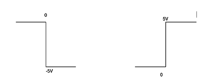
The integrator circuit as shown in the figure has R = 500K Ω and C=1µF. Find and plot the output voltage for the inputs as shown in the figure.
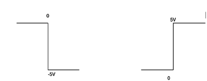
c)vi= 2 sin 4tV d) vi= 4tV
Solution:
We know that
v0 = - 1/RC  + v0(0)
Here R= 500K Ω and C = 1µF
1/RC = 1/ 500 x 1000 x 1 x 10-6
= 1/RC = 2
= -2  ; vi =- 5V
= -2 
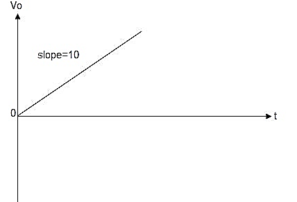
= 10t V
Which means it is a ramp voltage with positive slope.

When vi=5V
-2  ; vi = 5V
= -2 
= -10t V
Which means it is a ramp voltage with negative slope.
When vi= 2 sin4t V
Vo = -2 
= -4 [-cos 4t] /4
= cos 4t
When vi=4t V
Vo = 
= -8 [t2/2]
= - 4V
Key takeaway
For integrator
V0 = - 1/RC 
For differentiator

The Instrumentation amplifiers consist of three op-amps. In this circuit, a non-inverting amplifier is connected to each input of the differential amplifier.
This instrumentation amplifier provides high input impedance for exact measurement of input data from transducers. The circuit diagram of an instrumentation amplifier is as shown in the figure below.
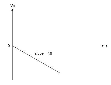
Fig: Instrumentation Amplifier
The op-amps 1 & 2 are non-inverting amplifiers and together form an input stage of the instrumentation amplifier. The op-amp 3 is a difference amplifier that forms the output stage of the instrumentation amplifier.
Working
The output stage of the instrumentation amplifier is a difference amplifier, whose output Vout is the amplified difference of the input signals applied to its input terminals.
If the outputs of op-amp 1 and op-amp 2 are Vo1 and Vo2 respectively, then the output of the difference amplifier is given by,
Vout = (R3/R2) (Vo1-Vo2)
The expressions for Vo1 and Vo2 can be found in terms of the input voltages and resistances.
Consider the input stage of the instrumentation amplifier as shown in the figure below.
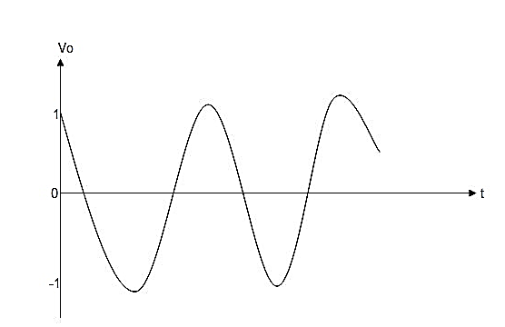
Fig. Input Stage of Instrumentation Amplifier
The potential at node A is the input voltage V1. Hence the potential at node B is also V1, from the virtual short concept. Thus, the potential at node G is also V1.
The potential at node D is the input voltage V2. Hence the potential at node C is also V2, from the virtual short. Thus, the potential at node H is also V2.
Ideally the current to the input stage op-amps is zero. Therefore, the current I through the resistors R1, Rgain and R1 remains the same.
Applying Ohm’s law between the nodes E and F,
I = (Vo1-Vo2)/(R1+Rgain+R1) ——————— 1
I = (Vo1-Vo2)/(2R1+Rgain)
Since no current is flowing to the input of the op-amps 1 & 2, the current I between the nodes G and H can be given as,
I = (VG-VH)/Rgain = (V1-V2)/Rgain ————————- 2
Equating equations 1 and 2,
(Vo1-Vo2)/(2R1+Rgain) = (V1-V2)/Rgain
(Vo1-Vo2) = (2R1+Rgain) (V1-V2)/Rgain —————— 3
The output of the difference amplifier is given as,
Vout = (R3/R2) (Vo1-Vo2)
Therefore, (Vo1 – Vo2) = (R2/R3)Vout
Substituting (Vo1 – Vo2) value in the equation 3, we get
(R2/R3)Vout = (2R1+Rgain) (V1-V2)/Rgain
i.e., Vout = (R3/R2) {(2R1+Rgain)/Rgain} (V1-V2)
The above equation gives the output voltage of an instrumentation amplifier. The overall gain of the amplifier is given by the term (R3/R2) {(2R1+Rgain)/Rgain}.
Key takeaway
References:
1. Microelectronics Circuits, Adel Sedra and Kenneth C Smith, Oxford University Press, New Delhi, 5th Edition, International Student Edition,2009. (Selected portion of Chapter 2,4, 5, 6, 8, 13, and 14)
2. Electronic Devices and Circuits theory, R.L. Boylestad and L. Nashelsky, Pearson Education, New Delhi, 9th/10th Edition,2013. (Selected portions of Chapter 4, 5, 6, 7, 8, 9, 10, 11, 12, and 14)
3. Milliman’s Electronics Devices and Circuits, J. Milliman, C. Halkias, S. Jit., Tata McGraw Hill